Integration of IoT and PCB

Strategic Integration of IoT and PCB Advancements for Defence Industry Expansion

The defence industry is changing fast. Across the UK and Europe, new threats and challenges mean that military systems must be smarter, faster, and more reliable. At the heart of this transformation is the powerful combination of IoT and advanced PCB technologies. If you’re involved in defence, you know that every detail matters, from the design of a single sensor to the reliability of a whole network. Let’s explore how printed circuit board manufacturers, IoT PCB design, and custom PCB assembly are driving the next generation of defence solutions.

Why IoT Matters in Defence

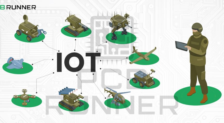
IoT, or the Internet of Things, means connecting devices so they can share data and work together. In defence, this is more than just a buzzword. IoT is already helping military teams track assets, monitor soldiers’ health, and manage complex operations in real time. Imagine a smart base where every piece of equipment, from vehicles to water pumps, reports its status automatically. Or a battlefield where sensors detect threats and share information instantly. This is possible because of reliable IoT PCB technology.

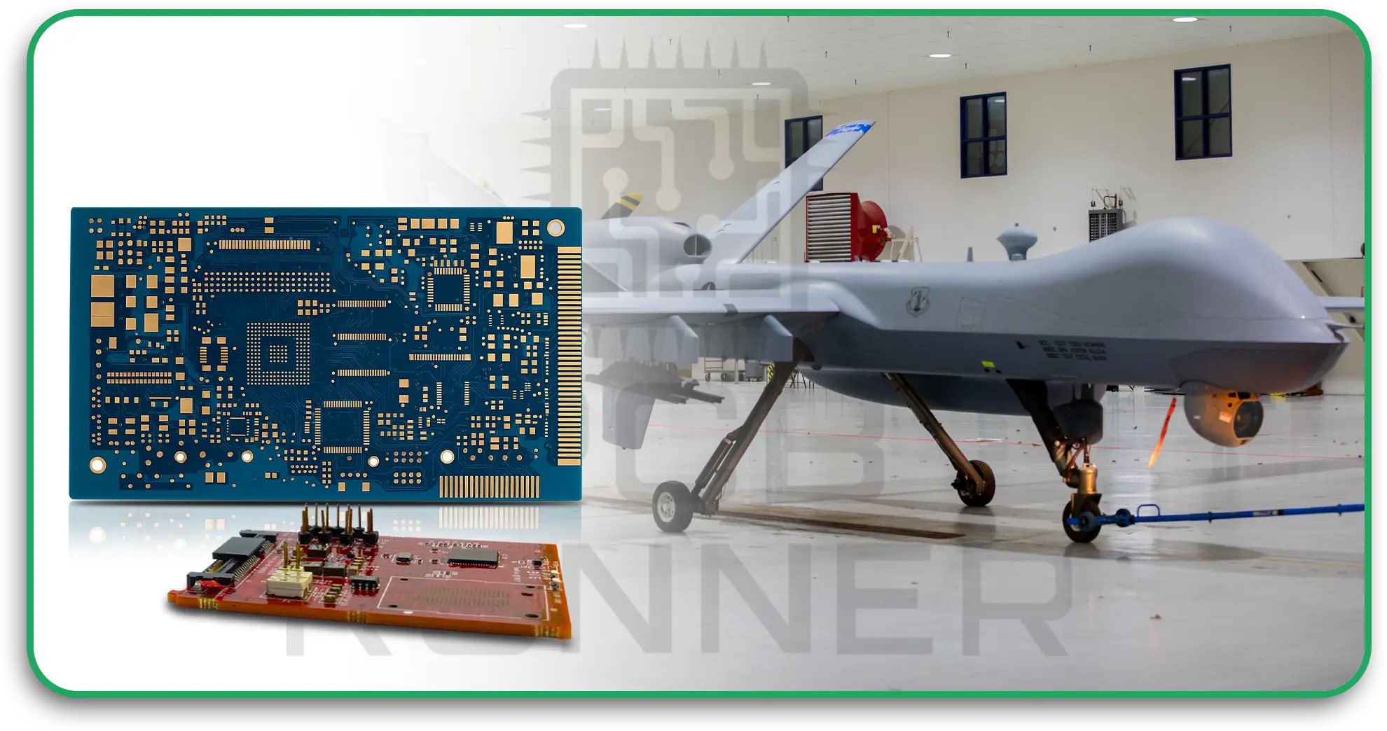
The Backbone: PCBs in Defence Applications

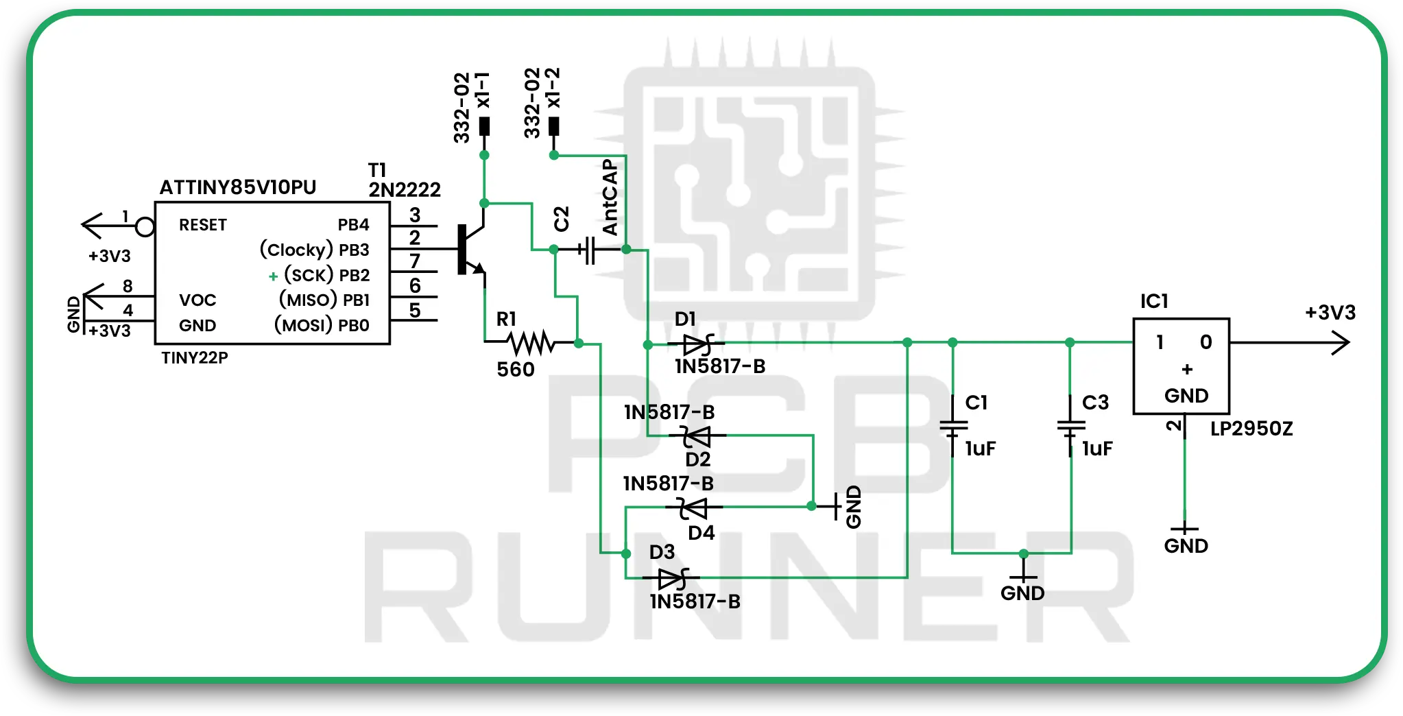
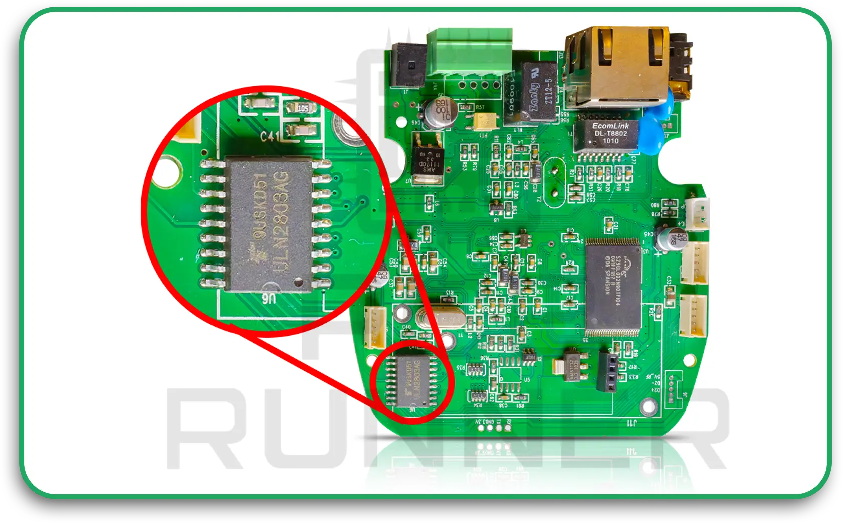
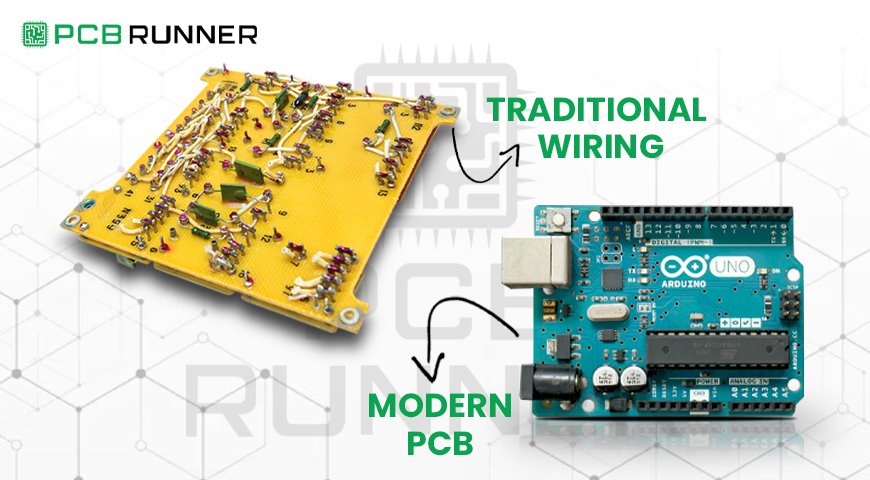
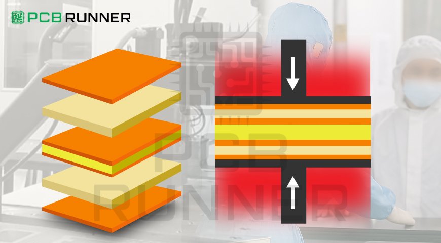
Printed circuit boards are the foundation of all modern electronics. In defence, they’re everywhere, from radios and radar systems to drones and missile guidance. Defence PCBs must be rigid, precise, and secure. They have to work in extreme temperatures, resist shock and vibration, and keep data safe. That’s why PCB manufacturing to defence standards is so important.

The Backbone_ PCBs in Defence Applications

Key Roles of PCBs in Defence:

  • Signal processing and secure data handling
  • Power management for mission-critical systems
  • Integrating sensors and communication modules
  • Enabling advanced guidance, navigation, and targeting

IoT PCB Design: Meeting Unique Defence Demands

IoT devices in defence need special PCBs. These boards must be small, lightweight, and energy-efficient, ut also strong enough for harsh environments. IoT PCB design is all about balance, packing in more features without sacrificing reliability.

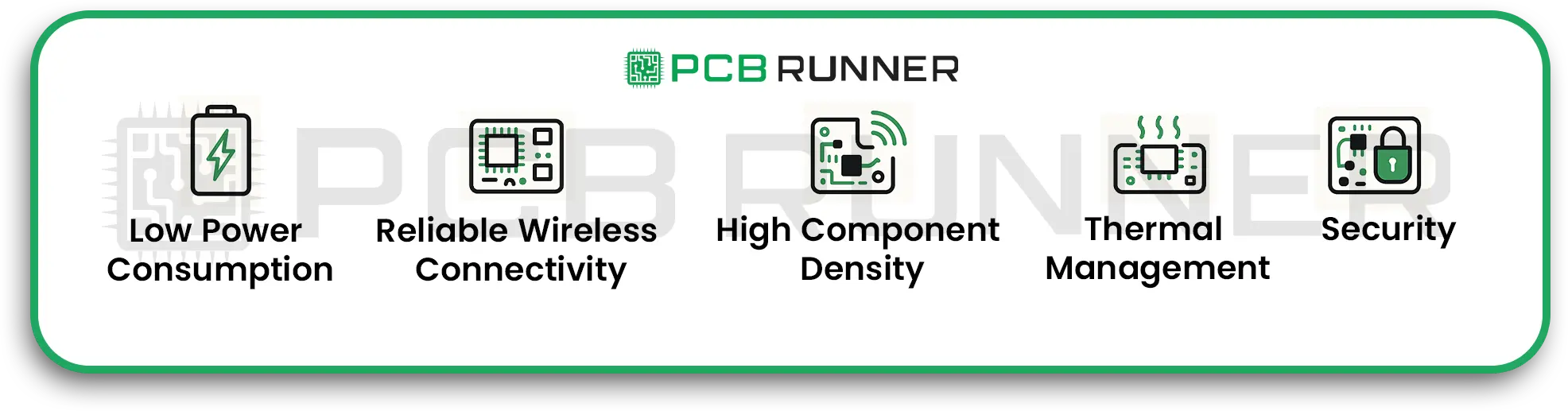
What Makes IoT PCBs Different?

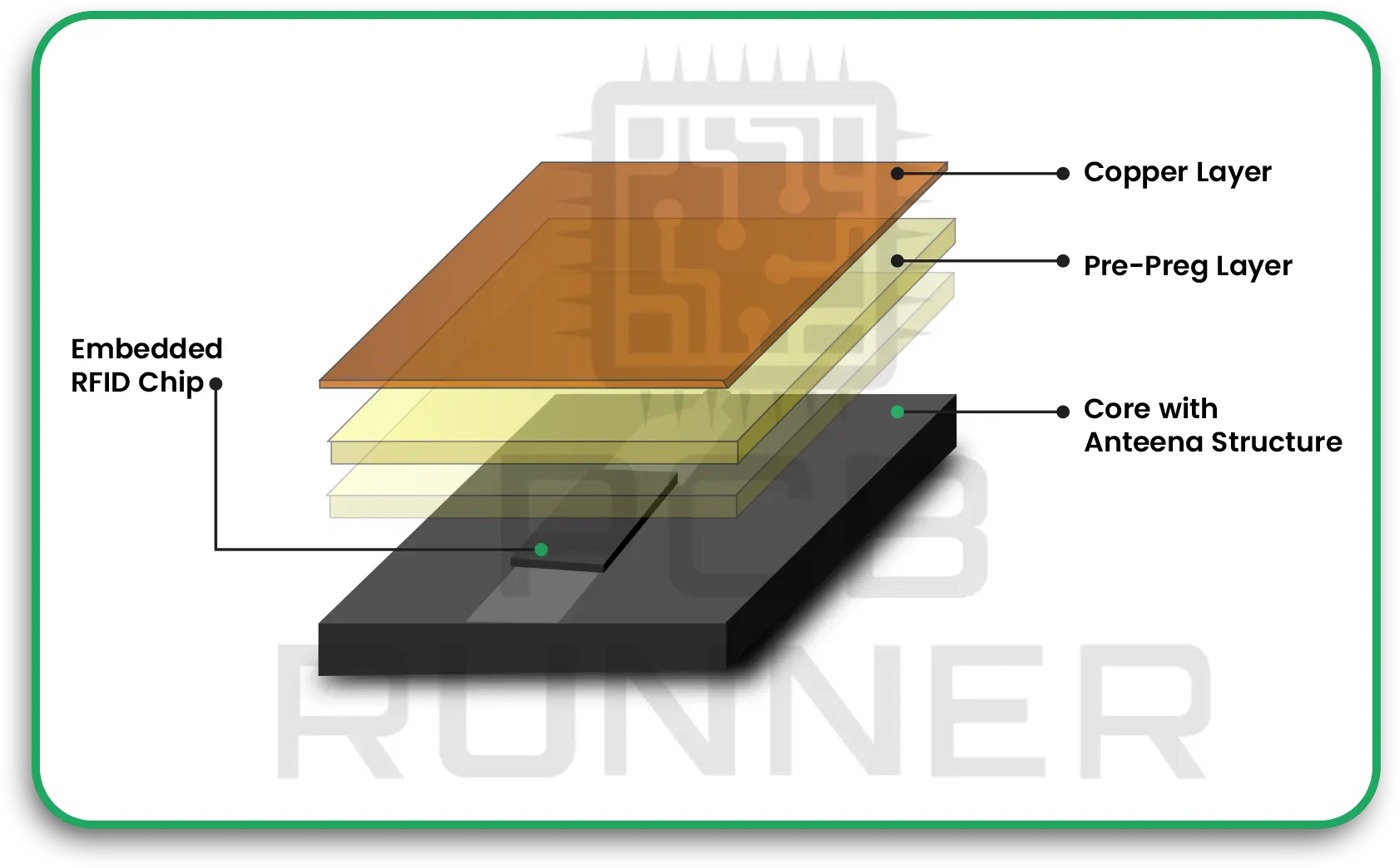
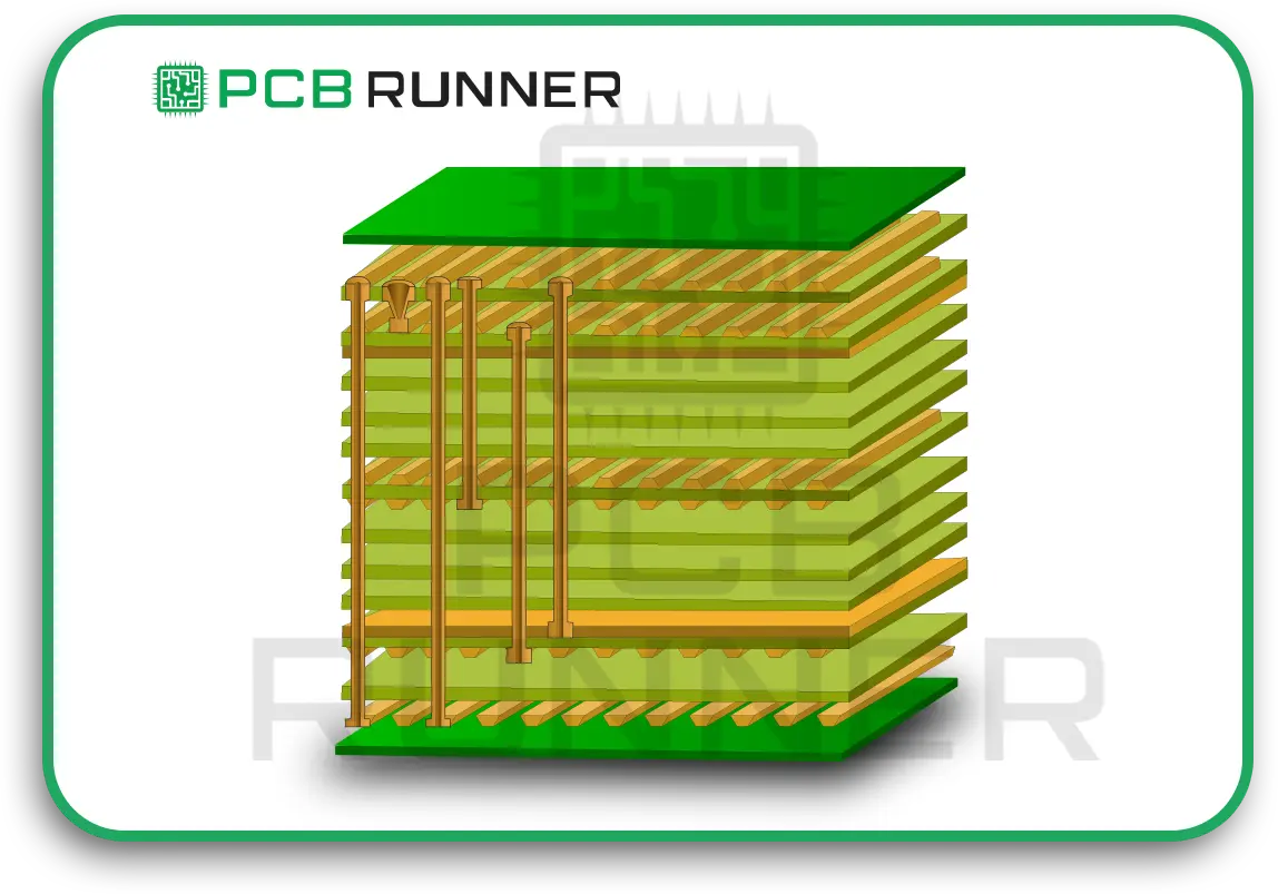
  • Miniaturisation: Defence systems need compact sensors and controllers. High-density PCB designs allow more connections in less space.
  • Power efficiency: IoT devices often run on batteries. Low-power PCB layouts help them last longer in the field.
  • Durability: IoT PCBs are coated and protected to survive dust, moisture, and extreme temperatures.
  • Security: Defence IoT PCBs must protect against hacking and data leaks, sometimes with hardware-based encryption.

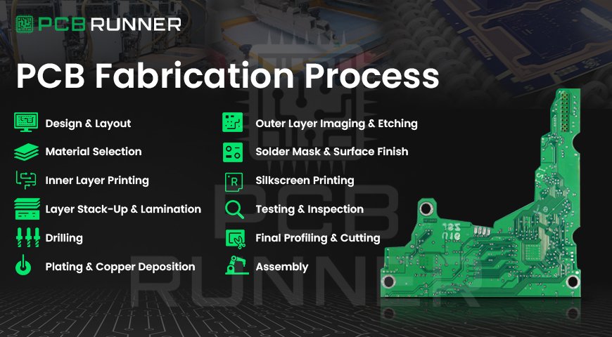
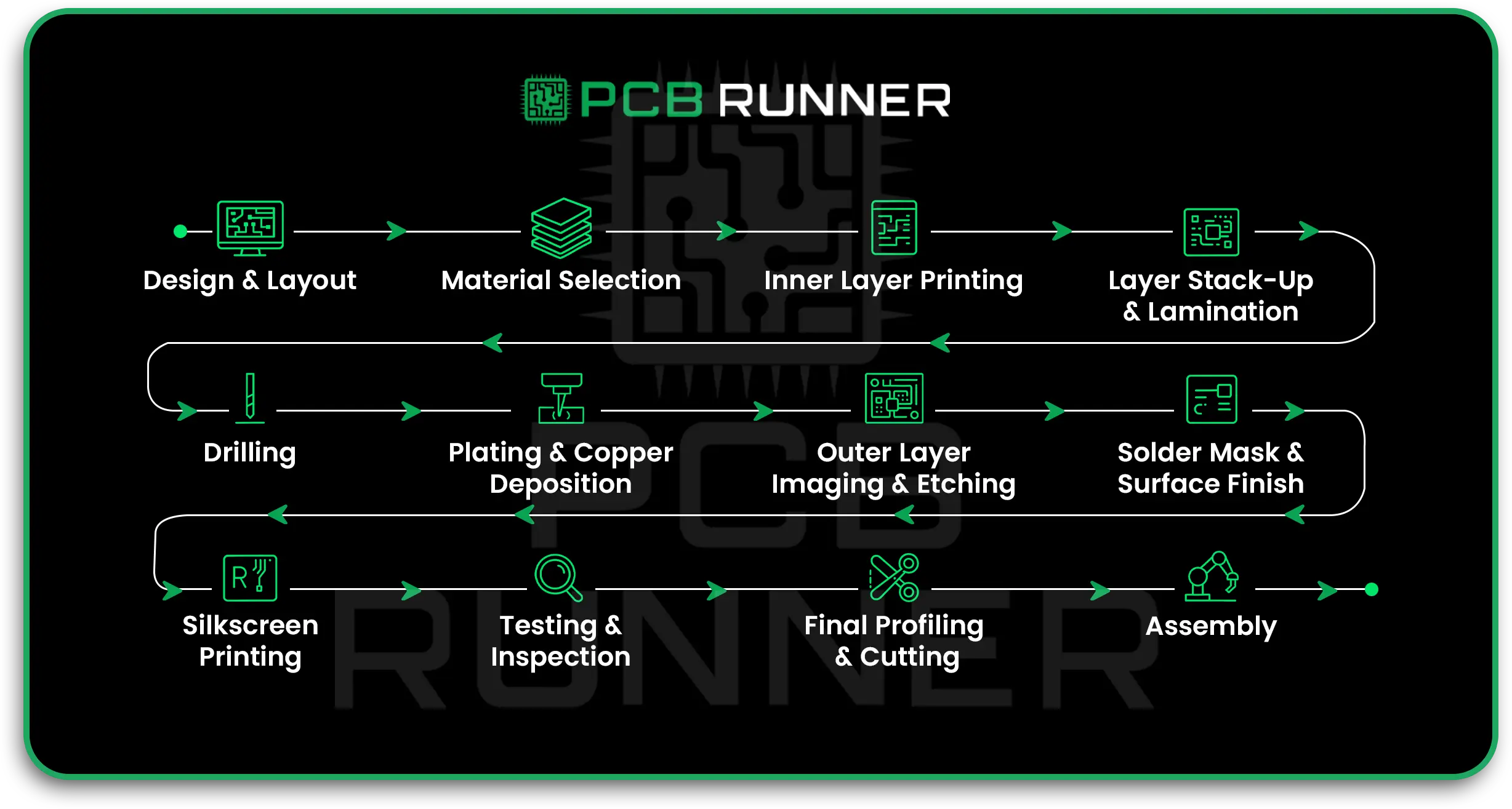
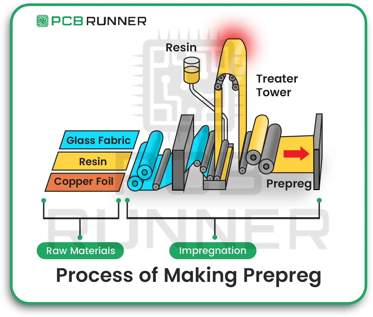
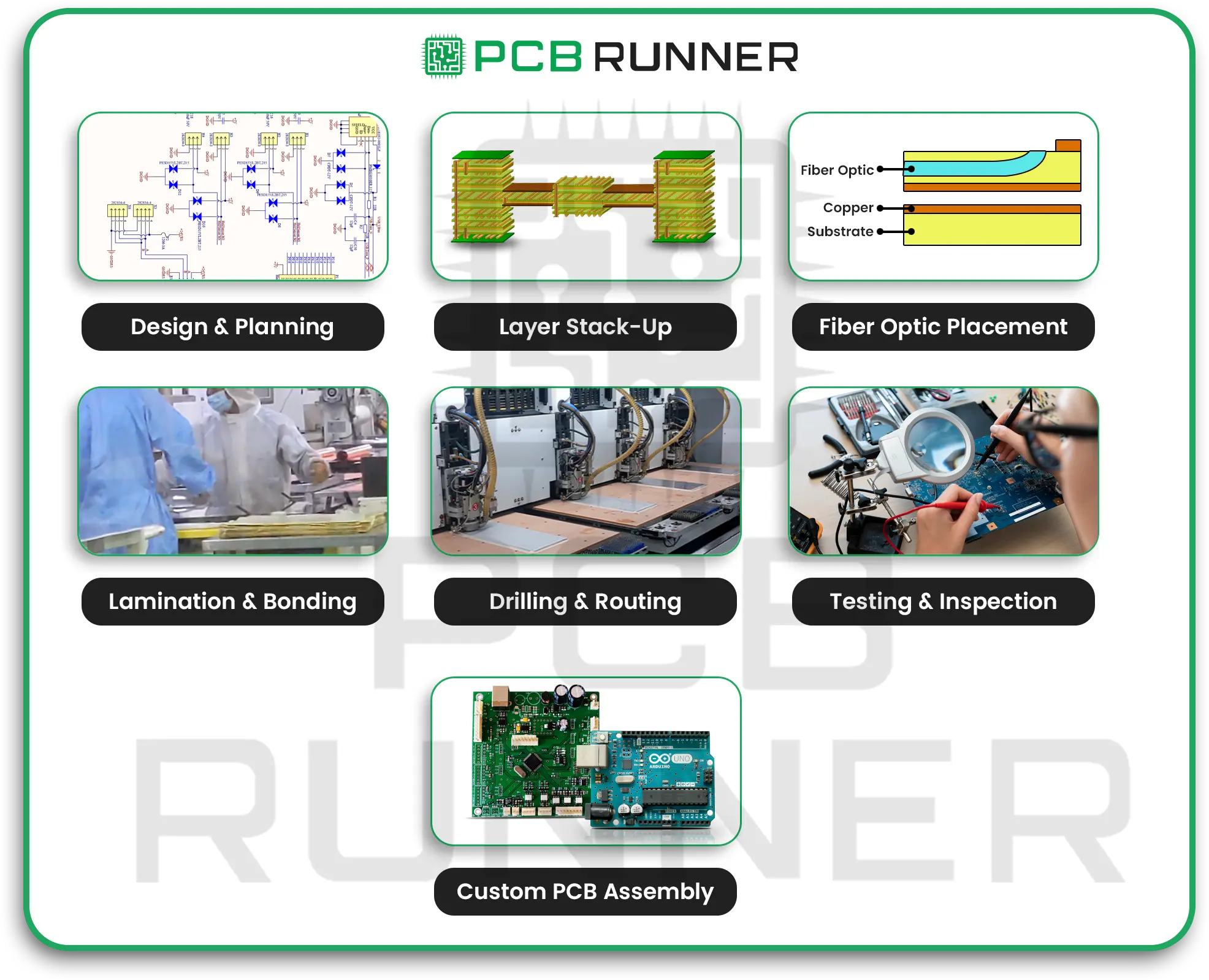
From Prototype to Production: The PCB Fabrication Journey

Every great defence device starts with a prototype. PCB prototype services let engineers test new ideas quickly. Once the design is proven, it moves to complete PCB fabrication in the UK or Europe. Here’s how it works:

  1. Design: Engineers create detailed IoT PCB designs, often using advanced simulation tools.
  2. Prototyping: Printed circuit board manufacturers build small batches for testing.
  3. Testing: Boards are checked for reliability, durability, and compliance with defence standards.
  4. Custom PCB Assembly: Once approved, the boards are assembled with components and prepared for deployment.

Choosing a partner with experience in PCB manufacture to defend standards is vital. They’ll understand the strict rules and quality checks needed for military use.

Custom PCB Assembly for Defence: Why It Matters

Defence projects rarely use off-the-shelf boards. Each mission has unique needs, from stealth drones to rugged vehicle controls. Custom PCB assembly lets you:

  • Select materials that resist heat, shock, and moisture
  • Add special coatings for electromagnetic shielding
  • Integrate IoT modules for real-time data sharing
  • Meet exact defence standards for safety and security

Real-World Applications: IoT and PCB Advancements in Action

Let’s look at how these technologies are making a difference:
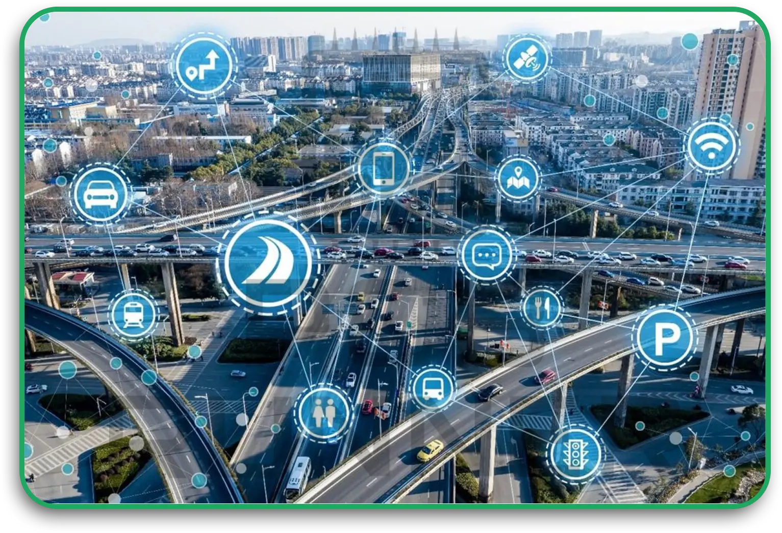
Smart Bases

Military bases use networks of IoT sensors to monitor water, power, and security. Each sensor needs a reliable IoT PCB to collect and send data. If a water pump fails or a gate is left open, the system alerts staff immediately.

Asset and Shipment Tracking

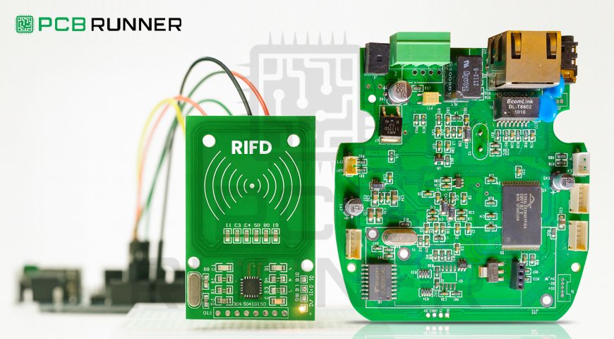
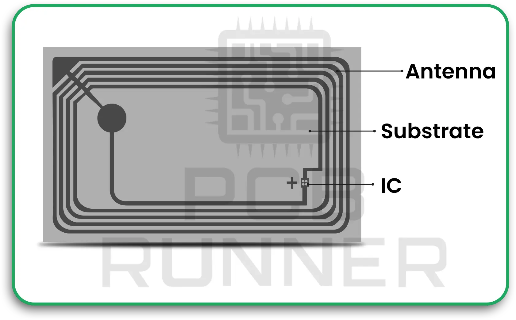
IoT PCBs in RFID tags and trackers help defence teams know exactly where weapons, vehicles, and supplies are at all times. This prevents loss and speeds up logistics.

Wearable Soldier Tech

Modern helmets and vests have built-in sensors to monitor health, location, and even stress levels. These wearables use miniaturised, ruggedised PCBs that can handle harsh conditions.

Advanced Weapon Systems

Guidance and targeting systems in missiles and drones depend on secure, high-performance PCBs. These boards process data from sensors, manage power, and keep communications safe from interference.

Meeting Defence Standards: What to Look For

Not all PCB fabrication is equal. Defence projects require boards that meet strict standards for quality, reliability, and security. When choosing a printed circuit board manufacturer for defence, check for:

  • Experience with military projects
  • Compliance with standards like MIL-STD-810
  • Ability to deliver rapid PCB prototypes and scale up to mass production
  • Custom PCB assembly with advanced testing and quality checks

Future Trends: Where IoT and PCB Technology Are Heading

The defence sector is constantly pushing the boundaries. Here’s what’s next:

  • AI Integration: Future IoT PCBs will include chips for artificial intelligence, enabling real-time analysis and smarter decision-making.
  • Flexible and Stretchable Boards: Wearable tech and conformal sensors will use flexible PCBs that bend and stretch with the user.
  • Radiation-Hardened Boards: For space and nuclear applications, special PCBs will resist radiation and extreme environments.
  • Sustainability: Defence agencies are looking for recyclable materials and energy-efficient manufacturing to reduce their environmental impact5.

Actionable Insights for Defence Teams

If you’re planning a new defence project, here’s how to get the most from IoT and PCB advancements:

  • Start with a clear goal: Know what you want your system to do, track assets, monitor health, or secure communications.
  • Work with experts: Choose printed circuit board manufacturers with a track record in defence and IoT PCB design.
  • Prototype early: Use PCB prototype services to test ideas quickly before moving to full production.
  • Insist on quality: Demand boards that meet defence standards for reliability and security.
  • Plan for the future: Design your systems so they can be upgraded as new IoT and PCB technologies emerge.

Final Thoughts

The strategic integration of IoT and PCB advancements is reshaping the defence industry across the UK and Europe. Reliable, secure, and innovative PCB technologies are the backbone of everything from smart bases to advanced weapon systems. By working with experienced partners in PCB Fabrication UK, focusing on IoT PCB design, and insisting on custom PCB assembly to defence standards, you can build systems that are ready for the challenges of tomorrow.

Whether you’re developing the next generation of wearable soldier tech or upgrading your base’s security network, remember: the right PCB makes all the difference. Choose wisely, and you’ll be ready for whatever comes next.

Integrating RFID

Exploring Methods of Integrating RFID with Printed Circuit Boards

If you’re curious about how modern electronics keep getting smarter, you’re not alone. One big reason is the use of RFID, or Radio Frequency Identification, in printed circuit boards (PCBs). Today, you’ll learn how RFID works, how it’s built into PCBs, and what it means for you as someone looking for the best circuit board suppliers UK or PCB circuit board manufacturers. We’ll also show you how custom PCB assembly with RFID can help your business, school, or project.

What is RFID and Why Should You Care?

RFID stands for Radio Frequency Identification. It’s a technology that uses radio waves to read and write information on small tags or chips. You see RFID everywhere, library books, store security tags, pet microchips, and even your school ID card. When you add RFID to a PCB, you get a device that can be tracked, managed, or even updated wirelessly.

Why does this matter to you?

  • You can track products easily.
  • You get better security for your devices.
  • You save time and money on inventory and repairs.

RFID Schematic

How Does RFID Work?

RFID has two main parts: a tag (which holds the chip) and a reader (which scans the tag). The tag contains an embedded RFID chip that stores information. The reader sends a signal, and the chip answers with its data.

Types of RFID Tags:

  • Passive tags: No battery. They get power from the reader’s signal.
  • Active tags: Have a battery. Used for longer distances.

When you put an embedded RFID chip into a PCB, you make the whole board “smart.” It can be tracked, locked, or unlocked with the right reader.

Why Embed RFID in a PCB?

You might wonder, “Why not just stick an RFID tag on the outside?” Here’s why having RFID embedded in PCB is better:

  • Security: The chip is hidden and hard to tamper with.
  • Space-saving: No bulky tags or stickers.
  • Durability: Protected from bumps, heat, and water.
  • Easy tracking: You can scan the board even when it’s inside a device.

Ways to Integrate RFID with Printed Circuit Boards

If you’re looking for PCB circuit board manufacturers or circuit board suppliers UK to help with RFID, here are the main ways they do it:

1. Surface Mounting

This is like putting any other chip on the board. The embedded RFID chip is soldered right onto the PCB surface. It’s fast and simple, but the chip is still visible and could get damaged if the board is handled roughly.

Surface Mounting

2. Embedding in PCB Layers

Here, the RFID chip or antenna is placed between the layers of the PCB during manufacturing. This keeps it safe and out of sight. It’s a popular choice for custom PCB assembly because it protects the chip and helps prevent tampering.

Embedding in PCB Layers

3. Antenna Etching

Some PCB circuit board manufacturers will etch the RFID antenna directly onto the board. This saves space and makes the board even thinner. The chip can be connected to this antenna, creating a complete RFID system inside the PCB.

Antenna Etching

4. Using RFID Modules

For larger projects or prototypes, you might use a small RFID module that plugs into your board. This isn’t as sleek as embedding, but it’s excellent for testing and learning how Radio Frequency Identification in PCB works.

Using RFID Modules (1)

What Does This Mean for You?

If you’re a business owner, student, or hobbyist, RFID embedded in PCB can help you:

  • Track parts and products in real-time
  • Prevent theft or loss by locking devices until they’re scanned
  • Speed up inventory and repairs
  • Make your products smarter and more valuable

Real-Life Uses for RFID in PCBs

You might be surprised how many things use Radio Frequency Identification RFID tags in PCBs. Here are some examples:

  • Retail: Stores use RFID to track electronics, shoes, and even clothing.
  • Healthcare: Hospitals track medical tools and devices to prevent loss.
  • Schools: Student ID cards and library books often have RFID chips.
  • Factories: Machines and tools are tracked for safety and repairs.
  • Access Control: Only people with the right RFID card can unlock doors or devices.

How to Get Started: What to Ask Your Supplier

When you talk to circuit board suppliers UK or PCB circuit board manufacturers about RFID, ask these questions:

  • Can you embed RFID chips or antennas in my PCB?
  • What size and type of RFID chip do you recommend?
  • How will the RFID chip affect my board’s performance?
  • Can you help with custom PCB assembly for my project?
  • What testing do you do to make sure the RFID works?

Step-by-Step: Adding RFID to Your PCB

Here’s a simple guide if you want to know how the process works:

  1. Choose Your RFID Type: Decide if you need passive or active RFID and what frequency range is best for your use.
  2. Design Your PCB: Work with your supplier to plan where the chip and antenna will go.
  3. Manufacture the Board: The supplier will build the PCB with the RFID chip embedded or mounted.
  4. Test the Board: Make sure the RFID tag works with your reader.
  5. Assemble Your Device: Use custom PCB assembly to add other parts and finish your project.
  6. Deploy and Track: Use RFID readers to scan and manage your boards in the real world.

Tips for Success with RFID Embedded in PCB

  • Plan Early: Talk to your supplier about RFID at the start of your project.
  • Test Often: Check the RFID function at each step, design, manufacturing, and assembly.
  • Think About Security: Use encrypted RFID chips if you’re worried about copying or hacking.
  • Keep It Simple: Start with a basic design and add more features as you learn.


RFID Integration Methods for PCBs

Method Description Best For Pros Cons
Surface Mounting Chip soldered on PCB surface Simple projects, prototypes Fast, easy to repair Chip is exposed
Embedded in Layers Chip or antenna inside PCB layers Secure, durable devices Hidden, protected More complex to make
Antenna Etching Antenna pattern etched onto PCB Thin, space-saving designs Saves space, sleek look Needs careful design
Plug-in Module RFID module attached to PCB Learning, testing, upgrades Easy to swap or replace Bulky, less secure

Final Thoughts

Adding RFID embedded in PCB is a smart move if you want to make your products easier to track, safer, and more efficient. Whether you’re building smart gadgets, managing inventory, or keeping your business secure, RFID gives you a significant advantage. The right PCB circuit board manufacturers can help you choose the best method, design your board, and make sure everything works as it should.

If you’re ready to take your project to the next level, reach out to trusted circuit board suppliers UK who understand Radio Frequency Identification in PCB. They’ll help you with custom PCB assembly, answer your questions, and make sure your boards are ready for the future.

Take the next step, explore RFID with your next PCB project and see how much easier life can be!

Frequently Asked Questions (FAQs)

Q1: What’s the difference between RFID and a barcode?
Barcodes need to be seen by a scanner, while RFID can be read through plastic or even inside a device. RFID tags can also store more information and can be updated wirelessly.

Q2: Can RFID chips be added to any PCB?
Most modern PCBs can have RFID chips embedded, but it’s best to plan for this during the design phase. Some very small or complex boards might need special solutions.

Q3: Are RFID chips safe from hackers?
Many RFID chips use encryption to protect your data. For extra safety, talk to your supplier about secure chips and best practices.

Q4: How far away can an RFID tag be read?
Passive tags work up to a few feet away. Active tags, which have batteries, can be read from much farther. The exact distance depends on the chip and reader.

Q5: Who can help me add RFID to my project?
Look for experienced PCB circuit board manufacturers or circuit board suppliers UK who offer custom PCB assembly with RFID. They can guide you through every step.

PCB Design

How to Accelerate the PCB Design Process Without Compromising Quality

If you’ve ever tried to design a printed circuit board, you know it can take a lot of time. There’s the planning, the drawing, the checking, and then the waiting for your board to be made. But what if you could speed up this whole process, without making mistakes or ending up with a poor-quality board? Good news: you can. Let’s walk through how you can accelerate your PCB design process while still getting a board you’re proud of.

Why Speed Matters in PCB Design

Getting your PCB done quickly means you can test your ideas sooner. If you’re working on a new gadget, every day counts. You want to be the first to launch, not the last. But if you rush and skip steps, you might end up with a board that doesn’t work. That’s why you need a plan that’s both fast and careful.

Start with a Clear Plan

Before you even open your design software, take a moment to think about what you need. What is your board supposed to do? How big should it be? What parts will you use? Write these things down. It helps you stay focused and avoid mistakes later.

  • Make a list of all the parts you need.
  • Decide how big your board should be.
  • Think about how your board will fit in your device.
  • Talk to your team so everyone knows the plan.

Clear Plan

Use the Right Tools

The software you use for PCB circuit design matters. Good tools let you work faster and spot problems before they become big headaches. Some design programs let you move easily from drawing your circuit to laying out your board. This saves time and reduces errors.

  • Use design tools that let you check your work as you go.
  • Look for software with built-in rules to catch mistakes.
  • Try to use the same tool for both the schematic and the PCB layout design.

Work with Experienced Printed Circuit Board Manufacturers

Not all printed circuit board manufacturers are the same. Some can make boards in just a day or two. Others take weeks. If you want to move fast, pick a company known for quick service and good quality. Ask them about their process and how they check for mistakes.

  • Choose a manufacturer with a solid track record.
  • Ask about their quality checks and delivery times.
  • Make sure they can handle your custom PCB design needs.

Don’t Skip Prototyping

You might think skipping the prototype step will save time. But if you do, you could end up with a board that doesn’t work, and that costs more time in the end. Quick-turn prototyping lets you test your design fast. If something’s wrong, you’ll catch it early.

  • Order a prototype before making lots of boards.
  • Use quick-turn services for faster results.
  • Test your prototype carefully.

Design for Manufacturing and Assembly

When you’re working on custom PCB assembly, think about how your board will actually be made. If your design is too tricky, it can slow down manufacturing or cause errors. Keep things simple and follow the rules your manufacturer gives you.

  • Use common part sizes and shapes.
  • Keep enough space between parts.
  • Avoid strange or hard-to-find components.
  • Follow your manufacturer’s guidelines for PCB board layout design.

Communicate with Your Assembly Team

If you’re using a PCB assembly UK service or any custom PCB assembly provider, talk to them early. Ask what files they need and what problems they see most often. This helps you avoid delays and makes sure your board is easy to assemble.

  • Share your plans and ask for feedback.
  • Double-check your files before sending them.
  • Be open to suggestions, they know what works best.

Use Templates and Standard Blocks

If you design a lot of boards, you probably use some of the same circuits over and over. Save time by making templates or reusable blocks. This way, you don’t have to start from scratch each time.

  • Save your favourite layouts for future use.
  • Build a library of standard circuits.
  • Use these blocks to speed up new projects.

Check Your Work, But Don’t Overthink It

It’s essential to check your design, but don’t get stuck in endless reviews. Use your software’s design rule checks to catch mistakes. Then, do a quick review with your team. If everything looks good, move forward.

  • Run the design rule check in your software.
  • Have a teammate look over your design.
  • Trust your process and keep moving.

Choose the Right Assembly Partner

Once your board is designed, you need someone to put it together. Look for a company that offers custom PCB assembly and has experience with boards like yours. If you’re in the UK, working with a PCB assembly UK company can save shipping time and make communication easier.

  • Pick a partner with a good reputation.
  • Ask about their assembly process.
  • Make sure they can handle your board’s size and complexity.

Keep Your Files Organized

Messy files slow everything down. Keep your design files, part lists, and instructions neat and easy to find. This helps your team and your manufacturer work faster.

  • Name your files clearly.
  • Keep everything in one place.
  • Double-check that your files match your design.

Learn from Each Project

After your board is done, take a few minutes to think about what worked and what didn’t. Did you hit your deadline? Were there any surprises? Use what you learn to do even better next time.

  • Write down what you’d change for next time.
  • Share tips with your team.
  • Keep improving your process.

Tips for Even Faster PCB Design

Here are some extra tips to help you speed things up:

  • Stay organized: Keep your workspace and files tidy.
  • Ask for help: If you get stuck, ask your team or your manufacturer.
  • Practice: The more boards you design, the faster you’ll get.
  • Use checklists: Make a list of steps and check them off as you go.

Final Thoughts

Speeding up your PCB design process doesn’t mean you have to cut corners. With a clear plan, the right tools, and good partners, you can move fast and still get a high-quality board. Remember to work with experienced printed circuit board manufacturers, use quick-turn prototyping, and communicate with your custom PCB assembly team. Keep your files organized, use templates, and always learn from each project.

You have what it takes to design great PCBs quickly. With these tips, you’ll be ready to tackle your next project, and get it done faster than ever.

Frequently Asked Questions

Q: How do I pick the right printed circuit board manufacturers?
A: Look for companies with good reviews, fast service, and strong quality checks. Ask about their experience with custom PCB design and PCB board layout design.
Q: What’s the best way to avoid mistakes in PCB circuit design?
A: Plan ahead, use good design tools, and check your work often. Don’t skip the prototype step.
Q: Can I speed up assembly with a PCB assembly UK company?
A: Yes. Local companies can often deliver faster and make it easier to fix problems if they come up.
Q: Should I use templates for custom PCB assembly?
A: Yes. Templates and reusable blocks save time and help you avoid repeating the same work.
Q: How can I make sure my custom PCB design is easy to assemble?
A: Use standard parts, keep enough space between components, and follow your assembly partner’s advice.

PCB Fabrication

Smart Innovations in the PCB Fabrication Process

Printed circuit boards (PCBs) are at the heart of every electronic device, from smartphones to satellites. As technology races ahead, the way we design and build PCBs is changing fast. The future is all about smart innovations, new materials, advanced machines, and clever software. In this blog, we’ll explore how the PCB fabrication process is evolving, especially in the UK, and what it means for businesses and engineers everywhere.

The Evolution of PCB Fabrication

PCB fabrication has come a long way, from simple single-layer boards to today’s complex, multi-layered designs. Modern PCB fabrication UK combines precision, speed, and creativity like never before.

What Is PCB Fabrication?

PCB fabrication is the process of making the physical board that holds and connects all the electronic parts. This includes choosing the right PCB circuit board material, layering, etching, drilling, and finishing the board so it’s ready for assembly.

PCB Fabrication Process

Advanced Materials, The New Building Blocks

The material of PCB is more important than ever. Today’s devices need boards that are strong, light, and can handle high speeds and heat. That’s why the choice of PCB board material is a big deal in modern PCB board fabrication.

Key Innovations in PCB Board Material

  • High-Performance Substrates: New substrates offer better heat resistance and electrical performance, perfect for 5G and high-speed devices1.
  • Conductive Inks: Used in additive manufacturing and 3D printing, these inks allow for more flexible and custom designs.
  • Biodegradable and Eco-Friendly Materials: These help reduce electronic waste and meet strict environmental rules.

Automation and AI, Smarter, Faster, Better

One of the most significant changes in PCB fabrication and assembly is the rise of automation and artificial intelligence (AI).

How Automation Is Changing PCB Fabrication UK

  • Automated Assembly Lines: Robots now handle soldering, component placement, and even inspection, making the process faster and more accurate.
  • AI-Driven Design: AI software helps design PCBs, optimizing layouts, checking for errors, and predicting failures before they happen.
  • Predictive Maintenance: AI keeps machines running smoothly by spotting problems before they cause downtime.

These smart-systems mean fewer mistakes, lower costs, and higher quality boards.

Automation Is Changing PCB Fabrication UK

3D Printing, A Game Changer for PCB Board Fabrication

3D printing isn’t just for plastic toys, it’s transforming how we make PCBs. With 3D printing, manufacturers can create complex shapes and custom boards quickly and with less waste.

Benefits of 3D Printed PCBs

  • Faster Prototyping: Engineers can test ideas in days, not weeks.
  • Customization: Each board can be made to fit special needs, great for aerospace or medical devices.
  • Cost Savings: Less material is wasted, and there’s no need for expensive moulds or tools.

Miniaturization and HDI, Packing More Into Less

As devices get smaller, PCBs must do more in less space. This is where High-Density Interconnect (HDI) technology comes in. HDI boards use tiny holes (microvias) and thin layers to fit more connections and parts into a smaller area.

Why HDI Matters

  • Supports Smaller Devices: Perfect for wearables, smartphones, and IoT gadgets.
  • Improved Performance: Better signal quality and less interference.
  • Greater Reliability: Fewer problems with heat and stress.

Eco-Friendly PCB Fabrication, Greener Boards for a Better Future

Sustainability is a big trend in PCB fabrication UK. Companies are looking for ways to make boards that are safer for people and the planet.

Green Innovations in PCB Board Material

  • Lead-Free and Halogen-Free Boards: Safer for workers and the environment.
  • Recyclable and Biodegradable Materials: Boards that break down or can be reused.
  • Energy-Efficient Production: Using less power and water and recycling waste.

Smart Testing and Quality Control

Making sure every board works perfectly is critical, especially for things like medical devices or aeroplanes. New testing methods use AI, robots, and real-time sensors to catch problems early and keep quality high.

Advanced Quality Control Methods

  • Automated Optical Inspection (AOI): Cameras and AI check every board for defects.
  • X-Ray Inspection: Finds hidden problems inside the board5.
  • IoT-Enabled Sensors: Monitor the process and alert teams if something goes wrong.

Embedded Components, The Next Step in PCB Assembly UK

Instead of placing all parts on the surface, new boards embed components inside the layers. This saves space, improves performance, and protects sensitive parts from damage.

Advantages of Embedded Components

  • Smaller, Lighter Boards: Perfect for drones, satellites, and medical implants.
  • Better Electrical Performance: Shorter paths mean faster signals and less noise.
  • More Durable: Components are shielded from shocks and moisture.

The Role of PCB Printed Circuit Board Assembly

After fabrication, the next step is pcb printed circuit board assembly. This is where all the chips, resistors, and other parts are added to the board. Smart machines and AI make this step faster and more reliable than ever.

Key Trends in PCB Assembly UK

  • Robotic Soldering: Ensures perfect joints every time.
  • Automated Placement: Tiny parts are placed with pinpoint accuracy.
  • Real-Time Quality Checks: Problems are caught and fixed on the spot.

Key Takeaways, Why Smart Innovations Matter

  • Automation and AI are making PCB fabrication and assembly faster, cheaper, and more reliable.
  • Advanced PCB board material choices mean better performance and greener electronics.
  • 3D printing and embedded components are opening new doors for design and miniaturization.
  • Quality control is more intelligent than ever, thanks to AI and real-time sensors.
  • The UK is at the forefront of these innovations, leading the way in innovative, sustainable PCB manufacturing.
Conclusion: The Future Is Now

The world of PCB fabrication in the UK is changing fast. Smart innovations, from new materials to AI-powered machines, are making boards smaller, faster, and greener. Whether you’re an engineer, a business owner, or just a tech fan, these changes mean better, more reliable electronics for everyone.

Ready to see what innovative PCB fabrication can do for your next project? The future is here, and it’s built on smarter boards.

FAQs, Your Questions About PCB Fabrication and Assembly

Q1: What is the most common PCB board material?
FR4, a type of fibreglass epoxy, is still the most common, but new materials like ceramics and biodegradable substrates are gaining ground.
Q2: How does AI help in PCB fabrication?
AI speeds up design, catches mistakes, and predicts failures before they happen, making the whole process smarter and more reliable.
Q3: Is 3D printing used for mass production of PCBs?
Right now, it’s mainly used for prototypes and small batches, but as the technology improves, it could become common for larger runs, too.
Q4: Why are eco-friendly materials necessary in PCB fabrication?
They help reduce toxic waste, protect workers, and meet strict environmental laws, making electronics safer for everyone.
Q5: What are the benefits of embedded components in PCBs?
They save space, improve performance, and protect sensitive parts from damage.

PCB Designs

From Past to Future: Trends in PCB Design

Printed circuit boards (PCBs) are the heart of modern electronics. From the first radios to today’s smart devices, PCBs have shaped how we live and work. In this blog, we’ll take you on a journey through the history of PCB design, explore today’s best practices, and look ahead at the future of PCB manufacture. Whether you’re curious about how to design PCB board layouts or want to know what’s next for the industry, this guide is for you.

The Early Days: How PCB Design Began

In the early days, PCBs were simple. They had just one layer and a few components. Designers drew circuits by hand, and PCB printing was a slow process. Most boards were large and bulky, used mainly in radios and early computers.

Key points from the past:

  • Manual drawing and etching
  • Single-layer boards
  • Slow, careful assembly

As technology advanced, so did the need for better PCB board layout design. This led to the rise of printed circuit board manufacturers who could make more complex boards faster and more reliably.

How to Design a PCB Circuit Board: The Basics

If you want to know how to design a PCB circuit board, start with the basics. The steps are much easier today, thanks to modern tools and guides.

Step-by-Step PCB Design Guide

  1. Define Your Goals: Know what your board needs to do. List all features and connections.
  2. Draw a Schematic: Use software to create a diagram of your circuit.
  3. Select Components: Choose the right parts for your design.
  4. Create the Layout: Arrange components on the board for the best performance.
  5. Route the Traces: Connect everything with copper lines.
  6. Check for Errors: Use design tools to find and fix mistakes.
  7. Prepare for Manufacturing: Export design files for PCB manufacture.
  8. Prototype and Test: Build a sample and make sure it works as planned.
  9. Final Adjustments: Fix any issues found during testing.
  10. Mass Production: Send your design to a trusted printed circuit board manufacturer for large-scale production.

Tips for beginners:

  • Start simple; use a basic pcb design guide.
  • Keep traces short and direct.
  • Group related parts together.
  • Double-check your work before printing.

Today’s Trends in PCB Board Layout Design

Modern PCB board layout design is more advanced than ever. Here’s what’s shaping the industry right now:

Miniaturization and High-Density Interconnects (HDI)

Devices are getting smaller and smarter. To keep up, pcb printing now uses HDI technology. This means more connections in less space, better performance, and lower power use. HDI is key for smartphones, wearables, and medical devices.

HDI and Miniaturization

Flexible and Rigid-Flex PCBs

New products need boards that can bend and twist. Flexible and rigid-flex PCBs are now common in cars, aeroplanes, and IoT devices. They fit into tight spaces and handle more stress without breaking.

Flexible and Rigid-Flex PCBs

Advanced Materials

PCB manufacturing is moving beyond traditional materials. Today’s boards use special plastics, graphene, and even biodegradable materials. These new options improve strength and heat resistance and are better for the environment.

Advanced Materials

3D PCB Printing

Additive manufacturing, or 3D printing, is changing how PCBs are made. It allows for fast prototyping and custom designs with less waste. This technology is beneficial for small batches and complex shapes.

3d printe pcb

Artificial Intelligence (AI) in PCB Design

AI is making a significant impact. It helps automate layout, checks for errors and even predicts problems before they happen. AI-powered tools are now part of every step, from design to quality control, making PCB manufacture faster and more reliable.

The Future of PCB Design

What’s next for PCB design? The industry is moving fast, and several trends are set to shape the future of PCB design:

  • Smaller, Smarter Boards: Miniaturization will continue with even more powerful boards in smaller spaces.
  • Eco-Friendly Manufacturing: More use of recyclable and non-toxic materials.
  • AI-Driven Design: Smarter tools that can design, test, and optimize boards automatically.
  • 3D and Additive Manufacturing: More use of 3D printing for both prototypes and final products.
  • Flexible Electronics: Boards that can stretch, bend, and even fold for new types of devices.

Why These Trends Matter

For anyone interested in how to design a PCB board or looking for a PCB design guide, understanding these trends is essential. They help you:

  • Create better, more reliable products
  • Reduce time and cost in development
  • Stay ahead in a fast-changing market

PCB Printing: Then and Now

Here’s a quick look at how PCB printing has changed over time:

Era Method Key Features Impact on Design
Early Days Manual drawing, etching Simple, single-layer Slow, error-prone
1980s-2000s Automated tools, CAD Multilayer, faster More complex designs
Today HDI, flexible, 3D printing Small, powerful, custom Fast, efficient, precise
Future AI, eco-materials, additive Smart, green, adaptable Smarter, sustainable

Best Practices for Modern PCB Board Layout Design

  • Plan Ahead: Define your goals and constraints early.
  • Use Ground and Power Planes: This reduces noise and improves stability.
  • Keep Traces Short: Shorter paths mean better performance.
  • Group Components: Place related parts close together.
  • Check Manufacturer Capabilities: Make sure your PCB manufacturing partner can handle your design’s complexity.
  • Test Early and Often: Prototype and test before full production.

Conclusion

PCB design has come a long way, from hand-drawn layouts to AI-powered, eco-friendly boards. Whether you’re new to electronics or an experienced engineer, staying updated on trends like HDI, flexible boards, and AI-driven tools will help you succeed. If you want to learn more about how to design a PCB board or need a reliable partner for PCB manufacture, keep exploring and stay ahead of the curve.

Ready to design your next PCB? Stay informed, use the latest tools, and partner with trusted printed circuit board manufacturers for the best results. The future of PCB design is bright and it’s just getting started!

Frequently Asked Questions (FAQs)

Q1: How do I start designing a PCB circuit board?
Begin with a clear schematic, choose your components, and use a simple PCB design guide to lay out your board. Many free tools are available to help beginners.

Q2: What is HDI in PCB design?
HDI stands for High-Density Interconnect. It allows more connections in a smaller area, making it perfect for compact devices like smartphones and wearables.

Q3: How is 3D printing changing PCB manufacture?
3D printing allows for fast prototyping and custom designs. It reduces waste and makes it easier to create complex shapes that were not possible before.

Q4: What are the benefits of flexible PCBs?
Flexible PCBs can bend and fit into tight spaces. They are durable and ideal for products that need to move or flex, like medical devices and wearables.

Q5: What is the future of PCB design?
The future of PCB design includes smarter, smaller, and more eco-friendly boards. AI and 3D printing will play a significant role, making design and manufacturing faster and more efficient.

PCB Technologies

Driving Smart Infrastructure Market Growth with Adaptive PCB Technologies

Imagine a world where cities are smarter, safer, and more efficient. Roads talk to cars, buildings manage their energy, and trains run on time with no delays. This isn’t the future, it’s happening now across the UK and Europe. At the heart of these changes are intelligent infrastructure systems powered by the latest technology in PCB design. If you’re curious about how adaptive PCB technologies are helping shape this new world, you’re in the right place.

What is Smart Infrastructure?

Smart infrastructure means using technology to make things work better. It’s about connecting roads, bridges, buildings, and even parks to the internet so they can collect and share information. This helps cities run smoothly, saves energy, and keeps people safe. But none of this is possible without reliable electronics. That’s where PCB circuit board manufacturers come in.

What is Smart Infrastructure

The Role of PCB Technologies

Printed circuit boards, or PCBs, are the backbone of all modern electronics. They connect all the tiny parts that make devices work. For smart infrastructure, you need PCBs that are tough, flexible, and packed with features. The latest technology in PCB design is making this possible.

Why Adaptive PCB Technologies Matter

Adaptive PCB technologies can change and improve as needs grow. For example, a high-density interconnect PCB lets engineers fit more connections in a smaller space. This is perfect for smart traffic lights or sensors that need to be small but powerful. Rigid-flex PCB manufacturers offer boards that bend and twist, which is excellent for devices that go in tight spaces or need to move.

How PCB Runner Supports the UK & Europe

If you’re looking for a reliable partner in the world of PCBs, PCB Runner stands out in the UK and Europe. With over 10 years of experience, they’ve built a reputation as a trusted PCB circuit board manufacturer1. They handle everything in-house, from design to assembly, so you get quality boards, fast turnaround, and excellent support.

Key Benefits of Choosing PCB Runner

  • All services are under one roof, no need to juggle different suppliers1.
  • Certified to ISO9001 and IPC Class 2, 3, and 3A standards, ensuring top quality1.
  • 24-hour tech support, so you always have help when you need it.
  • Free engineering file review before custom PCB fabrication, so you get precisely what you want.

Types of PCBs Making a Difference

Let’s look at some of the PCB technologies driving smart infrastructure:

High-Density Interconnect PCB (HDI PCB)

HDI PCBs are a game-changer. They let you pack more power into smaller devices. Think about sensors that monitor air quality or traffic flow in real-time. These sensors need to be tiny but must handle lots of data. HDI PCBs make this possible by using thinner lines and more layers.

Rigid Flex PCB Manufacturer Solutions

Some devices need to bend or fit into odd shapes, like smart wearables or curved displays on buses. Rigid-flex PCBs combine the strength of a rigid board with the flexibility of a thin, bendy one. This means your devices can go where traditional boards can’t.

Embedded PCB Technology

Embedded PCB technology puts chips and other parts right inside the board itself. This saves space and makes the board stronger. It’s perfect for devices that need to last a long time or work in tough places, such as underground sensors or railway controls.

Real-World Examples

Let’s see how these technologies are used in real life:

  • Smart Traffic Lights: These use HDI PCBs to process data from cameras and sensors. They can change signals based on real-time traffic, reducing jams and pollution.
  • Energy Management in Buildings: Embedded PCB technology helps control heating, lighting, and security from a single system. This saves energy and keeps people comfortable.
  • Railway Safety: Rigid-flex PCBs are used in train control systems. They’re tough enough to handle vibrations and flexible enough to fit into tight spaces.

Why Quality Matters

In smart infrastructure, failure isn’t an option. A single faulty board can cause delays, safety risks, or even accidents. That’s why it’s essential to work with a PCB circuit board manufacturer that puts quality first. PCB Runner reviews every engineering file before production and offers after-sales support to solve problems quickly.

How to Choose the Right PCB Partner

If you’re planning an innovative infrastructure project, here’s what to look for in a PCB partner:

  • Experience in the UK and Europe, with a proven track record1.
  • Ability to handle both small and large orders so that you can scale up as needed1.
  • Certified quality standards for peace of mind1.
  • Fast, friendly customer service, including 24-hour tech support1.

PCB Runner ticks all these boxes, making them a top choice for engineers and project managers.

The Future of Intelligent Infrastructure Systems

As cities get smarter, the demand for advanced PCB technologies will only grow. Here’s what you can expect in the coming years:

  • Even smaller and more powerful HDI PCBs for next-generation sensors.
  • More use of embedded PCB technology for rugged, long-lasting devices.
  • Flexible and rigid flex PCBs in everything from smart streetlights to wearable tech for workers.

Actionable Tips for Your Next Project

If you’re starting a new smart infrastructure project, keep these tips in mind:

  • Plan for the Future: Choose PCB technologies that can adapt as your needs change.
  • Work with Experts: Partner with a manufacturer like PCB Runner who understands the challenges of intelligent infrastructure systems.
  • Focus on Quality: Don’t cut corners, invest in boards that are built to last.
  • Ask for Support: Make sure your supplier offers technical help when you need it.

Final Thoughts

Smart infrastructure is changing the way we live, work, and travel. The latest technology in PCB design is making it all possible. Whether you need a high-density to interconnect PCB for a tiny sensor, a rigid-flex PCB manufacturer for a flexible device, or embedded PCB technology for a tough job, the right partner makes all the difference.

PCB Runner has earned the trust of customers across the UK and Europe by delivering quality, reliability, and support1. If you want your smart infrastructure project to succeed, start with the best in PCB technologies.

Ready to take the next step? Reach out to PCB Runner for a free quote and see how they can help you build the future, one board at a time.

Laminate Materials

The Future of PCB Design: Advancements in Laminate Materials

Printed circuit boards (PCBs) are the unsung heroes of modern electronics. From smartphones to satellites, they connect and power the devices we rely on every day. But as our technology advances, so must the materials and methods used in PCB manufacture and design. One of the most exciting areas of innovation is in PCB laminate materials. In this blog, we’ll explore how new laminate materials are shaping the future of PCB fabrication, especially in the UK, and what this means for industries everywhere.

PCB Laminate Materials: The Foundation of Modern Electronics

Before we dive into the future, let’s start with the basics. PCB laminate materials are the backbone of every circuit board. They provide the structure, strength, and electrical insulation needed for reliable performance. Think of them as the canvas on which your electronic masterpiece is built.

What Are Laminate Materials for PCB Fabrication?

A PCB laminate is typically made from layers of fiberglass and resin pressed together to form a solid, durable sheet. The most common type is FR4, a glass-reinforced epoxy laminate. It’s strong, lightweight, and affordable—making it the go-to choice for many applications.

But as devices get faster and smaller, traditional laminates can’t always keep up. That’s where new materials come in.

Process of Making Prepreg lamination

Why Laminate Materials Matter in PCB Manufacture

The choice of PCB laminate materials affects everything from signal speed to heat resistance. In high-speed or high-frequency circuits, even tiny losses can cause big problems. That’s why industries like telecom, aerospace, and automotive are demanding better, more innovative materials.

Key Properties of Advanced PCB Laminates

  • Low dielectric loss: Keeps signals strong and clear.
  • High heat resistance: Prevents warping and failure under stress.
  • Mechanical strength: Withstands bending and vibration.
  • Environmental safety: Reduces toxic waste and supports recycling.

Key Properties of Advanced PCB Laminates

Latest Trends in PCB Laminate Materials

The world of PCB fabrication UK is changing fast. Let’s look at some of the trends shaping the future.

1. High-Performance Substrates

New high-performance substrates, like advanced epoxies and polyimides, offer better thermal and electrical properties. These materials are perfect for demanding applications, such as 5G networks and automotive radar.

2. Low-Loss Dielectric Materials

For high-frequency designs, low-loss dielectrics are a game changer. Materials like PTFE (Teflon) and special ceramics allow signals to travel faster, with less distortion. This is crucial for hdi pcb board designs, where space is tight, and performance is critical.

3. Eco-Friendly and Recyclable Laminates

Sustainability is becoming a top priority. New bio-based and recyclable laminates, like JIVA’s Soluboard®, are being tested by major companies for their ability to reduce e-waste and support responsible manufacturing7. These materials dissolve in hot water, making it easier to recover valuable components and metals at end-of-life.

4. 3D Printing and Additive Manufacturing

3D printing is transforming the fabrication of printed circuit boards. With conductive inks and printable laminates, manufacturers can create complex, custom boards with less waste and faster turnaround times. This is especially useful for prototyping and small-batch production.

The Role of HDI PCB Board Technology

High-density interconnect (HDI) PCB boards are leading the miniaturization revolution. By using thinner laminates and microvias, HDI boards pack more power into less space. This technology relies on advanced laminate materials that can handle tight tolerances and high signal speeds.

HDI PCB Board Technology

Benefits of HDI PCB Boards

  • Smaller size: Perfect for wearables, smartphones, and IoT devices.
  • Better performance: Supports high-speed, high-frequency signals.
  • Greater reliability: Reduces risk of defects and failures.


Comparing Traditional vs. Advanced PCB Laminates

Feature Traditional FR4 Advanced Laminates (PTFE, Polyimide, Ceramic)
Dielectric Constant Moderate Low (better for high-speed)
Heat Resistance Good Excellent
Environmental Impact Non-recyclable Some are recyclable or biodegradable
Cost Low Higher, but dropping as tech matures
Use Cases General electronics 5G, aerospace, automotive, HDI

How PCB Laminate Innovations Impact PCB Printed Circuit Board Assembly

Advancements in PCB laminate materials don’t just improve the board—they also make PCB-printed circuit board assembly faster and more reliable. With better laminates, soldering is easier, components stay put, and the finished board is less likely to fail in the field.

Real-World Example

Imagine assembling a high-speed router for a 5G network. Using a low-loss, high-heat laminate means the board can handle fast data without overheating or dropping signals. That’s a win for both manufacturers and users.

Sustainability: The Next Frontier in PCB Fabrication UK

The push for greener electronics is driving change in the PCB fabrication UK sector. Manufacturers are adopting:

  • Lead-free and halogen-free laminates: Safer for workers and the environment.
  • Energy-efficient production: Using renewable energy and recycling water.
  • Biodegradable substrates: Reducing landfill waste and supporting circular economies.

These changes are not just good for the planet—they also help companies meet strict regulations and appeal to eco-conscious customers.

The Future: What’s Next for PCB Laminate Materials?

The future looks bright—and busy. Here’s what to watch for:

AI and Automation in PCB Design

AI-powered tools are making it easier to choose the right laminate for each project. These systems can predict how different materials will perform, optimize layouts, and even spot potential problems before production begins.

Embedded Components

New laminates allow for components to be embedded directly into the board, saving space and improving reliability. This trend is significant for medical devices, aerospace, and automotive electronics.

Custom and On-Demand Fabrication

With 3D printing and advanced laminates, it’s now possible to create custom boards on demand. This means faster prototyping, less waste, and more flexibility for designers and engineers.

Key Takeaways: Why Laminate Innovation Matters

  • PCB laminate materials are the foundation of every electronic device.
  • Advancements in laminates enable faster, smaller, and more reliable PCBs.
  • Eco-friendly and recyclable materials are shaping the future of PCB Fabrication UK.
  • AI, automation, and 3D printing are making custom, high-performance boards more accessible than ever.
  • Choosing the right laminate is key to success in modern PCB manufacture and assembly.

Conclusion: Building the Future, One Layer at a Time

The world of PCB laminate materials is evolving fast. As technology pushes boundaries, so do the materials and methods behind every circuit board. Whether you’re designing for speed, sustainability, or both, the right laminate can make all the difference.

At the heart of this change is a simple truth: better materials mean better electronics. For anyone involved in PCB manufacture, PCB fabrication UK, or PCB printed circuit board assembly, staying ahead of these trends is the key to building the next generation of smart, sustainable devices.

Ready to take your PCB designs to the next level? Explore the latest in laminate materials and see how innovation can power your next big idea.

FAQs: Your Questions About PCB Laminate Materials Answered

Q1: Why are laminate materials so necessary in PCB manufacture?
Laminate materials determine the strength, speed, and reliability of a PCB. The right choice ensures your board can handle high speeds, heat, and stress without failing.
Q2: What’s the difference between FR4 and advanced laminates?
FR4 is a standard, affordable option. Advanced laminates like PTFE or ceramics offer better performance for high-speed or high-frequency applications but may cost more.
Q3: Are eco-friendly laminates as reliable as traditional ones?
Yes, many new eco-friendly laminates match or even exceed the performance of traditional materials. Companies like Microsoft and Jaguar are already testing them in real-world products.
Q4: How do new laminates affect the fabrication of printed circuit boards?
They make boards easier to assemble, more reliable, and better suited for demanding applications like 5G, IoT, and automotive electronics.
Q5: What’s next for PCB laminate materials?
Expect more recyclable, biodegradable, and high-performance options, along with more brilliant AI-driven design and on-demand manufacturing.

Telecom Equipmen

Empowering the Telecom Equipment Market with Advanced PCB Innovations

Ever wondered what keeps your phone calls crisp, your internet fast, and your smart devices connected? The answer lies in a tiny yet mighty hero: the printed circuit board, or PCB. In today’s fast-paced telecom equipment market, advanced PCB innovations are driving change and powering the networks we rely on every day. Let’s dive into how PCB manufacturing is shaping the future of telecom and why companies like PCB Runner are leading the way in the UK and Europe.

PCB Manufacture – The Backbone of Telecom Equipment

Printed circuit boards are at the core of every telecom device. From mobile towers to home routers, they make sure signals travel smoothly, and data gets where it needs to go. But not all PCBs are created equal. In the telecom equipment market, quality and reliability are everything.

Why Quality Matters in PCB Production UK

Telecom networks can’t afford downtime. Every second counts. That’s why telecom PCB assembly must meet strict standards. At PCB Runner, we don’t just manufacture PCBs; we ensure every board is tested, certified, and ready for action. Our ISO9001 certification and IPC Class 2, 3, and 3A qualifications mean you get peace of mind with every order.

Why Quality Matters in PCB Production UK

Key Features of Reliable Telecom PCB Assembly

  • Consistent Quality: In-house manufacturing ensures every PCB meets our high standards.
  • Quick Turnaround: Fast production, whether you need a single prototype or a large batch.
  • Comprehensive Support: 24-hour tech support for all your questions and concerns.
  • Custom PCB with Components: Tailored solutions for unique telecom needs.

pcb runner

Advanced Materials – Powering Next-Gen Telecom

The telecom equipment market is changing fast, especially with the rollout of 5G and the rise of smart devices. This shift demands more from every PCB board component. Advanced materials are now essential for high-speed, high-frequency communication.

The Role of Exotic Materials in PCB Production UK

Modern telecom PCBs use materials like PTFE and high-frequency laminates. These help reduce signal loss, improve speed, and boost overall performance. As networks move to 5G and beyond, these innovations are no longer optional; they’re a must-have.

Benefits of Advanced PCB Board Components

  • Better Signal Integrity: Less loss, clearer connections.
  • Higher Speeds: Perfect for 5G, IoT, and AI-driven devices.
  • Improved Durability: Withstands heat and stress in demanding environments.

Custom PCB with Components – Tailored for Telecom

No two telecom projects are the same. That’s why custom PCB with components is a game-changer. Whether it’s a complex switching system or a compact router, custom solutions ensure every need is met.

PCB Runner’s Approach to Customization

We work closely with customers to design, review, and assemble PCBs that fit their exact requirements. Our team checks every engineering file before production, ensuring you get precisely what you expect, no surprises, just results.

Customization Advantages

  • Flexibility: From rigid to flex and rigid-flex designs.
  • Precision: Every detail is tailored to your application.
  • Cost-Effectiveness: Optimized for both performance and budget.

Trends Shaping the Telecom PCB Assembly Market

The telecom equipment market is booming, and so is the need for advanced PCB solutions. Here are some trends you should know:

High-Density Interconnect (HDI) PCBs

HDI PCBs pack more circuits into less space. This is crucial as telecom devices shrink but need more power and speed. HDI technology is at the forefront of modern telecom PCB assembly.

Eco-Friendly Manufacturing

Sustainability matters. Many telecom companies now demand eco-friendly PCB production UK, using recyclable materials and greener processes. PCB Runner is committed to these practices, helping customers meet both performance and environmental goals.

Eco-Friendly Manufacturing

Growing Demand for Telecom PCB

With 5G networks expanding and IoT devices multiplying, the need for reliable telecom PCB is skyrocketing. The global telecom PCB market is set to grow at over 6% annually, driven by new technologies and rising data demands.

Growing Demand for Telecom PCB

Why Choose PCB Runner for Your Telecom PCB Needs?

Choosing the right partner for PCB manufacture can make or break your telecom project. Here’s why PCB Runner stands out:

One-Stop Shop for PCB Production UK

  • All Services Under One Roof: From design to assembly, we handle it all.
  • Instant Quotes: Get pricing and place orders any time, day or night.
  • After-Sales Support: We’re here for you, even after delivery.

Trusted by Industry Leaders

Our customers include major players in telecom, defence, medical, and more. Many come to us through word-of-mouth, thanks to our reputation for reliability and quality.

The Future of Telecom Marketing and Equipment

  • Advanced PCB innovations are powering the telecom equipment market.
  • Quality, speed, and customization are critical for telecom PCB assembly.
  • Eco-friendly and high-density PCB solutions are shaping the future.
  • PCB Runner is your trusted partner for PCB Production UK, offering expertise, reliability, and support.

Conclusion: Building Tomorrow’s Networks Today

The telecom equipment market is evolving at lightning speed. At the heart of this change? Advanced PCBs that make everything possible. Whether you need a single prototype or a full production run, PCB Runner is here to help. We bring together the best in PCB manufacture, PCB printed circuit board assembly, and custom solutions, so you can focus on what matters: connecting the world.

Ready to power up your next telecom project? Get in touch with PCB Runner for a free quote and see how we can help you lead the way in telecom innovation.

FAQs – Your Telecom PCB Questions Answered

Q1: What makes a telecom PCB different from a regular PCB?
A telecom PCB is built to handle high-frequency signals and large amounts of data. It uses special materials and designs to ensure reliability and speed.
Q2: How fast can I get a custom PCB with components?
At PCB Runner, we offer quick turnarounds for both prototypes and production runs. Timelines depend on complexity, but we’re known for fast, reliable delivery.
Q3: Are eco-friendly PCBs available for telecom applications?
Yes, We use recyclable materials and sustainable processes to meet both performance and environmental needs.
Q4: Can you help with design and assembly?
Absolutely. Our team reviews your files, offers design advice, and assembles your PCBs, all under one roof.
Q5: What industries do you serve besides telecom?
We supply PCBs for military, aerospace, defence, medical, and more. Any industry needing high-quality, reliable PCBs can count on us.

Optical Layers in PCB

Inside the Innovation: Optical Layers in PCB Manufacturing

When you look at your phone, a computer, or even a modern car, you probably don’t think about the tiny highways inside that move information at lightning speed. But those highways, built into printed circuit boards (PCBs), are what make today’s fast, smart devices possible. And now, with optical layers joining the mix, those highways are getting faster and more reliable than ever.

If you’re curious about how optical layers work in PCB manufacture, or you want to know what it means for your next project, you’re in the right place. Let’s break down what makes optical integration so important, how fibre optic printed circuit boards are built, and why this matters for you and your business.

What Are Optical Layers in PCBs?

Traditional PCBs use copper traces to carry signals. These traces are like tiny roads for electricity. But as our need for speed grows, think faster internet, better streaming, and smarter machines, copper sometimes hits its limits. That’s where optical layers come in.

Optical layers use light instead of electricity to move information. Inside the board, you’ll find fibre optic interconnects or special optical channels. These can carry more data faster and with less interference. It’s a bit like swapping out a busy city street for a high-speed train, suddenly, everything moves quicker and smoother.

Why Use Optical Integration PCB Technology?

Let’s keep it simple. Here are the main reasons you might want optical layers in your PCB printed circuit board assembly:

  • Speed: Light travels faster than electricity, so you get quicker data movement.
  • Bandwidth: Optical interconnects can handle more information at once.
  • Less Noise: Optical signals aren’t bothered by electrical interference.
  • Distance: Fiber optic interconnects can send signals further without losing quality.

If you’re building telecom equipment, servers, or anything that needs to move lots of data, these benefits are a big deal.

Why Use Optical Integration PCB Technology_

How Optical Layers Fit into PCB Manufacture

Adding optical layers to a PCB isn’t just about sticking in a few extra parts. It’s a careful process that starts at the design stage and goes all the way through custom PCB assembly. Here’s how it usually works:

Design and Planning

First, you and your team decide where you need optical channels. Maybe you want to connect two chips that are far apart, or you need to link several boards together with fibre optic interconnects. You’ll work with your PCB manufacturing partner to plan the layout and choose the right materials.

Layer Stack-Up

A modern PCB can have many layers, some for power, some for signals, and now, some for light. The optical layers are often sandwiched between regular copper layers. This keeps everything compact and protected.

Fiber Optic Placement

During the build, technicians place tiny fibre optic cables or waveguides into the board. These need to be lined up perfectly so the light can travel without getting lost. It’s a bit like threading a needle but with much smaller threads.

Lamination and Bonding

Once everything is in place, the layers are pressed together using heat and pressure. This step locks the optical and electrical parts into a single, solid board.

Drilling and Routing

Special machines drill holes and create paths for both the copper and optical parts. Precision matters, if a hole is off by even a fraction of a millimetre, the light won’t travel correctly.

Testing and Inspection

Before the board is finished, it’s checked with automated tools. These tools look for problems in both the electrical and optical layers. If something’s wrong, it’s fixed before moving to the next step.

Custom PCB Assembly

Finally, your board moves to assembly. Here, chips and other components are added, and everything is soldered in place. If you’re working with a partner like PCB Runners, they’ll make sure your optical integration PCB is handled with care from start to finish.

How Optical Layers Fit into PCB Manufacture

Where Are Fiber Optic Printed Circuit Boards Used?

You might be surprised at how many places use optical layers today:

  • Telecom equipment: Fast, reliable data transfer is a must.
  • Data centres: Servers need to talk to each other quickly.
  • Medical devices: High-resolution images and fast data movement help doctors and patients.
  • Aerospace: Secure, interference-free signals are critical in planes and satellites.

If you’re in any of these fields, you know how important speed and reliability are. Optical layers help you meet those goals.

Tips for Working with Optical Interconnects in PCBs

If you’re thinking about adding optical layers to your next PCB prototype or product, here are some things to keep in mind:

  • Work with experienced partners: Not every PCB shop can handle optical layers. Choose a team that knows the process inside and out.
  • Plan your layout carefully: Optical channels need straight, clear paths. Avoid sharp bends or crowded areas.
  • Choose the right materials: Some PCB materials are better for light transmission than others.
  • Test early and often: Catching problems early saves time and money later.
  • Document everything: Good notes help your team and your PCB manufacturing partner avoid mistakes.

Real-World Example: Building a Fiber Optic PCB Prototype

Let’s say you’re designing a new telecom switch. You need to move massive amounts of data between different parts of the board. Using only copper would mean thick, heavy traces and lots of heat. By adding optical layers, you can keep your board slim, cool, and fast.

You start by working with your PCB manufacturing partner to design the stack-up. You add fibre optic interconnects between key chips. After building a PCB prototype, you test it thoroughly. The results? Faster speeds, better reliability, and a product that stands out in the telecom equipment market.

Conclusion: Why Optical Layers Matter for Your Next Project

Optical layers are changing the way we think about PCB manufacture and custom PCB assembly. By using light instead of just electricity, you can build boards that are faster, more reliable, and ready for the future. Whether you’re working on a PCB prototype or a full-scale product, fibre optic printed circuit board technology gives you a real edge.

At PCB Runners, we’re here to help you every step of the way, from design to PCB printed circuit board assembly. If you’re ready to take your next project to the next level, consider adding optical layers. Your devices will be faster, smarter, and ready for whatever comes next.

Frequently Asked Questions

1. What is an Optical Integration PCB?
It’s a printed circuit board that uses both copper and optical layers to move data. The optical parts use light, usually through fibre optic channels.
2. How do fibre optic interconnects work in a PCB?
They act like tiny light pipes, carrying signals from one part of the board to another with little loss or interference.
3. Can I get a PCB prototype with optical layers?
Yes. PCB Runners offers prototyping services so you can test your design before full production.
4. Are optical layers only for big companies?
No. As costs come down, more businesses, big and small, are using optical integration in their products.
5. What are the main challenges with optical layers?
Precision is key. Misalignment or poor material choices can cause problems, so it’s important to work with experts.
6. Do I need special equipment to test optical layers?
Yes. Automated optical inspection tools are used to check alignment and quality.
7. How do optical interconnects help with custom PCB assembly?
They let you connect more parts in less space, making your boards more powerful and compact.
8. Where should I start if I want to use optical layers?
Contact a trusted PCB manufacturing partner like PCB Runners early in your design process.

Internet of Things

The Future is Connected: Inside the Internet of Things

The Internet of Things (IoT) is changing the way we live and work. From smart thermostats and fitness trackers to industrial sensors and connected vehicles, IoT devices are everywhere. But what makes these devices possible? At the heart of every IoT device is a carefully engineered printed circuit board (PCB). The right PCB design and production choices are what allow IoT devices to be small, efficient, and reliable.

If you want to understand where IoT is heading and how to build devices that stand out, you need to know how Multilayer PCB, Flex and Rigid PCB, and smart PCB production methods make it all work. Let’s break down the key technical details and best practices for designing PCBs for the Internet of Things.

Understanding IoT PCB Requirements

IoT devices come in many forms, but they all have a few things in common. They need to be compact, often run on battery power, and must connect wirelessly. That means the PCB inside must be designed for low power, high density, and strong wireless performance.

Here’s what you need to focus on when working with IoT PCB design:

  • Low power consumption: Most IoT devices use batteries. The PCB must help minimise power draw to extend battery life.
  • High component density: Space is limited, so you need to fit more components into a smaller area.
  • Reliable wireless connectivity: The board must support antennas and RF circuits without causing interference.
  • Thermal management: Even small devices generate heat. Good PCB design keeps temperatures under control.
  • Security: Many IoT devices handle sensitive data. Hardware security features can be built into the PCB.

Understanding IoT PCB Requirements

Multilayer PCB: The Foundation for Complex IoT Devices

As IoT devices get smaller and more powerful, a single-layer PCB often isn’t enough. Multilayer PCB technology stacks several layers of circuitry, separated by insulating material, into one compact board. This approach allows you to:

  • Route more signals in less space
  • Separate analogue and digital signals to reduce interference
  • Improve power distribution and grounding
  • Support high-speed data and wireless signals

For example, a smart thermostat might use a Multilayer PCB to keep the Wi-Fi, processor, and sensor circuits separate, reducing noise and improving reliability2. In industrial IoT, Multilayer PCBs are essential for handling complex control and communication tasks.

Flex and Rigid PCB: Adapting to Any Shape or Space

IoT devices don’t always come in neat rectangles. Wearables, medical sensors, and automotive IoT often need PCBs that bend, fold, or fit into unusual spaces. That’s where Flex and Rigid PCB designs come in.

  • Flex PCBs are made from flexible materials, allowing them to bend and twist without breaking. They’re perfect for devices that need to fit into tight or curved spaces.
  • Rigid-Flex PCBs combine rigid sections (for mounting chips and connectors) with flexible sections (for folding or bending). This design reduces the need for connectors and cables, saving space and improving reliability.

Flex and Rigid PCB technology lets you design devices that are lighter, more durable, and more comfortable to wear or use.

PCB Production for IoT: What Matters Most

The best IoT devices depend on high-quality PCB production. Here are the most important factors to consider:

  • Material selection: Choose materials that match your device’s needs. For example, flexible substrates for wearables or high-frequency laminates for wireless modules9.
  • Precision manufacturing: IoT PCBs often use High-Density Interconnect (HDI) techniques, such as microvias and fine trace widths, to fit more into less space.
  • Quality control: Consistent production is key. Even small defects can cause big problems in small devices.
  • Customisation: Every IoT application is different. PCB production should allow for custom shapes, sizes, and features.

Best Practices for PCB Design for the Internet of Things

To get the most from your IoT PCB, follow these proven design strategies:

1. Optimise Layer Stack-Up

Use multiple layers to separate power, ground, and signal traces. This reduces noise and improves signal integrity, especially for wireless and high-speed circuits.

2. Minimise Trace Lengths

Shorter traces mean less signal loss and a lower risk of interference. Keep sensitive signals as short as possible, and use controlled impedance routing for high-speed or RF signals.

3. Plan for Power Efficiency

Choose low-power components and use power-saving design techniques. For example, use sleep modes for microcontrollers and sensors, and minimise the number of active circuits at any time.

4. Manage Heat

Even small IoT devices can get hot. Use thermal vias, copper pours, and a good component layout to spread and remove heat.

5. Support Reliable Wireless Connections

Keep antennas and RF circuits away from noisy digital signals. Use proper grounding and shielding to reduce electromagnetic interference (EMI).

6. Ensure Security

If your device handles sensitive data, consider adding hardware security modules or secure elements directly to the PCB.

7. Design for Manufacturability

Follow DFM (Design for Manufacturability) guidelines to make sure your board can be produced at scale, with minimal errors and rework.

Best Practices for PCB Design for the Internet of Things

Real-World Example: Smart Home Sensor

Let’s say you’re designing a smart home sensor. You’d likely use a Multilayer PCB to separate the power, processor, and wireless circuits. If the sensor needs to fit in a small or curved case, a Flex PCB makes sense. You’d keep trace lengths short, use microvias for high density, and make sure the antenna is isolated from digital noise. The result? A sensor that’s small, reliable, and lasts for years on a single battery.

Challenges in IoT PCB Design

Designing PCBs for IoT isn’t without its hurdles:

  • Signal integrity: High-frequency signals are sensitive to noise and interference. Careful routing and grounding are a must.
  • Component placement: With so many parts in a small space, placement is critical for both performance and manufacturability.
  • Testing and validation: Each device must be tested for power use, wireless range, and durability.
  • Cost control: Advanced features like Multilayer PCB and Flex and Rigid PCB add cost. Balance performance with budget for your application.

The Future of IoT PCB Design

As IoT continues to grow, PCB design and production will keep evolving. Expect to see:

  • Even higher density layouts, thanks to new HDI and micro via technology
  • More use of Flex and Rigid PCB designs for wearables and medical devices
  • Better integration of security and wireless features at the hardware level
  • Smarter, more automated PCB production for faster turnaround and lower costs

Key Takeaways

  • IoT devices depend on advanced PCB design and production for performance, size, and reliability.
  • Multilayer PCB and Flex and Rigid PCB technologies are essential for fitting more features into smaller, more complex devices.
  • Good PCB design for the Internet of Things focuses on power efficiency, signal integrity, thermal management, and manufacturability.
  • As IoT grows, so will the need for innovative PCB production methods and materials.

If you’re building for the future, start with the right PCB. It’s the foundation that makes every connection possible.

Conclusion: PCB Runners and the Connected Future

The Internet of Things is transforming every industry, from smart homes to healthcare to industrial automation. At the heart of this transformation are advanced PCBs—especially Multilayer PCB, Flex and Rigid PCB, and rigid HDI substrates—that make it possible to pack more features, better connectivity, and higher reliability into smaller, more efficient devices. 

Careful PCB design for Internet of Things applications is essential for meeting the strict demands of power efficiency, wireless performance, and durability that modern IoT devices require.

PCB Runners stands out as a leader in this space, delivering PCB solutions that support the unique needs of IoT innovation. Their expertise in rigid HDI PCB fabrication, power distribution, and signal integrity ensures that your IoT devices are not only compact and efficient but also robust enough for real-world use.