PCB Assembly Mistakes

Top PCB Assembly Mistakes and How to Avoid Them

Building a PCB, or printed circuit board, assembly is a bit like putting together a puzzle. Every piece needs to fit just right. If you miss a step, the whole thing can fall apart. From the initial idea to the final board assembly, numerous opportunities exist for things to go wrong. But don’t worry, most problems are easy to spot and fix if you know what to look for.

Below, you’ll find the most common mistakes in PCB assembly and simple ways to avoid them. Whether you’re new to circuit board assembly or you’ve done it a hundred times, these tips will help you get better results every time.

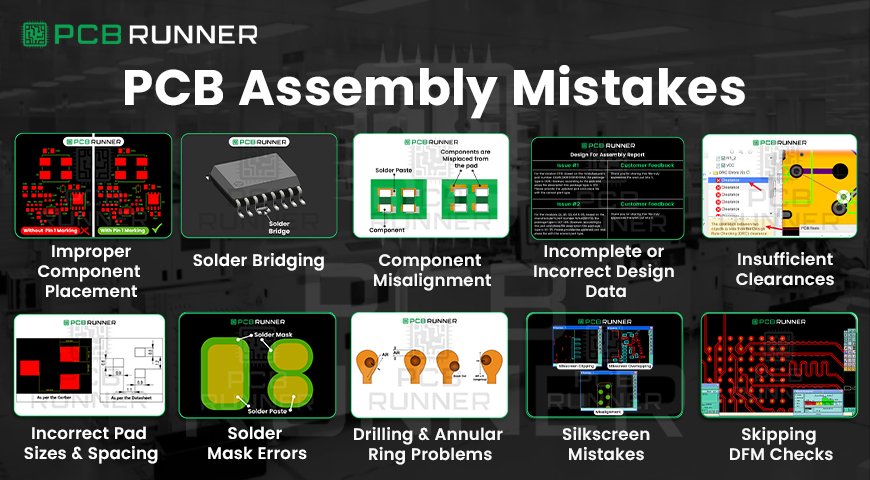
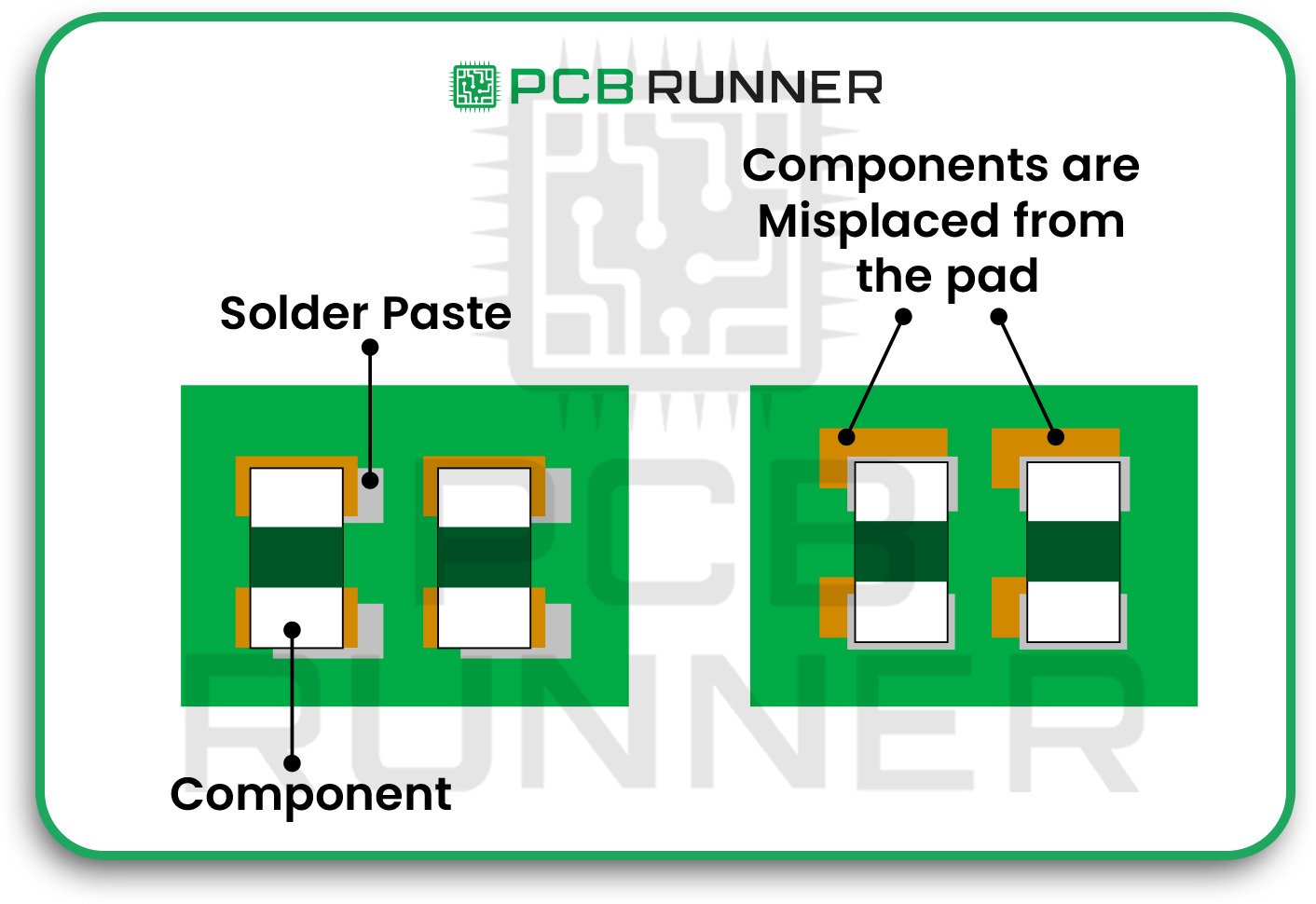
1. Improper Component Placement

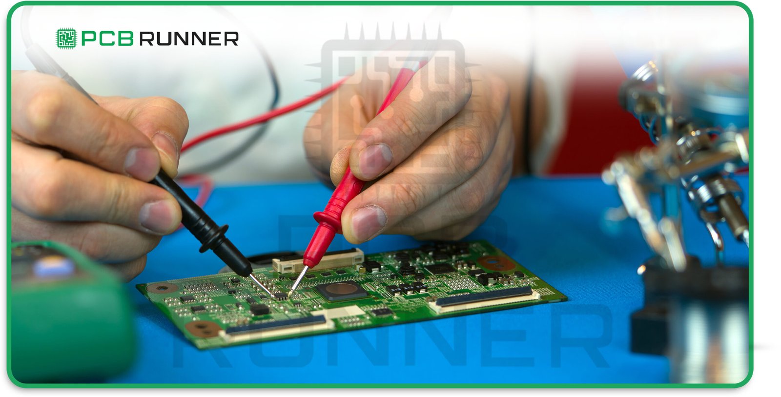
One of the biggest mistakes in PCB assembly is putting parts in the wrong place. Even a minor mix-up can cause short circuits, signal problems, or even damage the board.

How to avoid it:

  • Double-check your design files before starting.
  • Use PCB design software to visualise the layout of your board.
  • Pay close attention to part orientation, look for pin one or polarity marks.
  • After assembly, do a visual inspection to catch any misplaced parts.
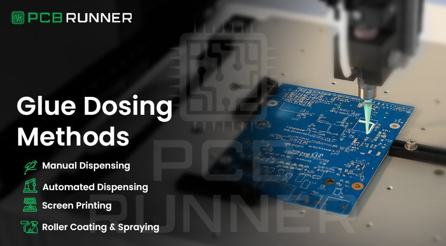
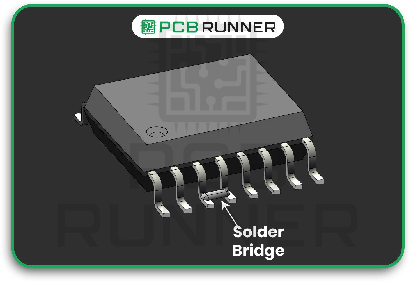
Improper Component Placement

2. Solder Bridging

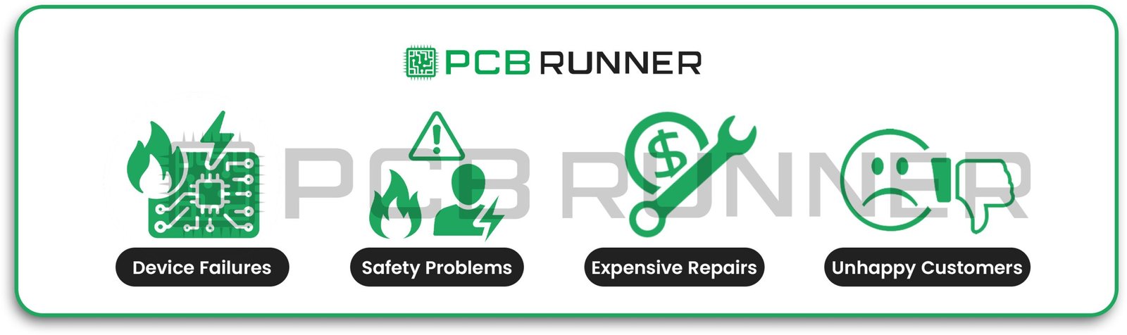
Solder bridging occurs when excess solder creates a connection between two pads or traces that shouldn’t be in contact. This can cause short circuits and device failures.

How to avoid it:

  • Use the right amount of solder paste.
  • Make sure your solder stencil has proper openings and spacing.
  • Inspect your PCB prototype or finished board for solder bridges.
  • Use a solder wick or sucker to fix any bridges you find.

Solder Bridging

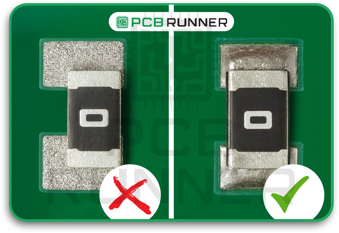
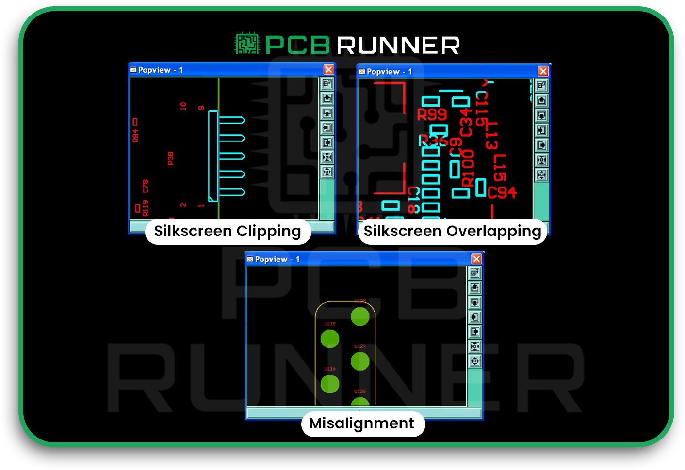
3. Component Misalignment

If a part isn’t aligned with its pads, it may not form a good connection. This can cause weak joints, signal issues, or even make the part fall off later.

How to avoid it:

  • Calibrate your pick-and-place machines regularly.
  • Use support systems to keep the board steady during the assembly process.
  • Check placement accuracy before soldering.
  • Do regular maintenance on your assembly equipment.

Component Misalignment

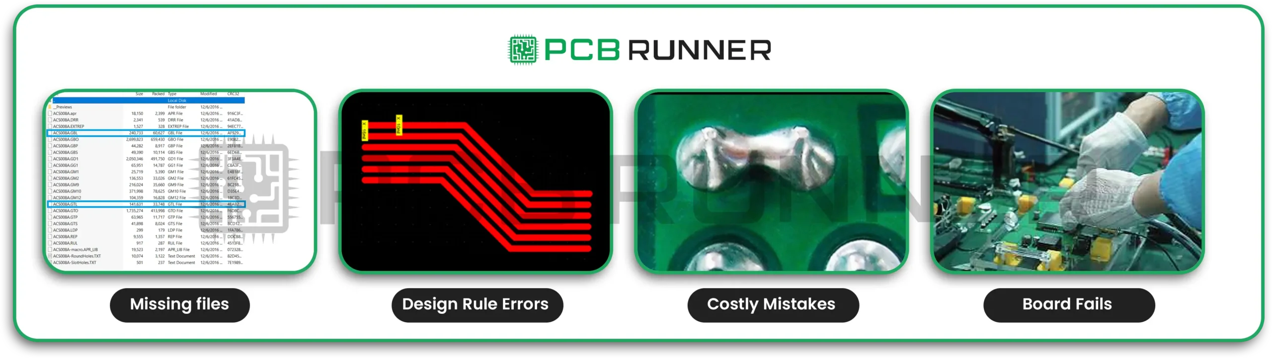
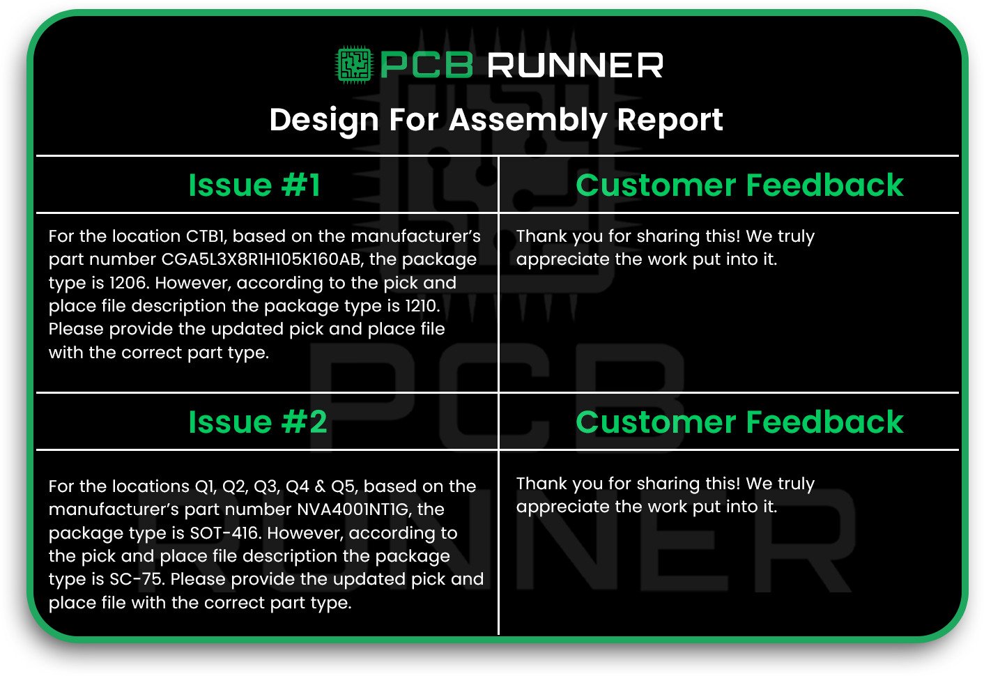
4. Incomplete or Incorrect Design Data

If your assembly team doesn’t have all the correct information, mistakes are bound to happen. Missing or unclear drawings, wrong part numbers, or missing polarity marks can all lead to trouble.

How to avoid it:

  • Provide precise, complete assembly drawings.
  • Include all part references, values, and special instructions.
  • Ensure that polarity and pin one marks are clearly visible on your silkscreen.
  • Double-check that your assembly notes match your PCB fabrication assembly files.

Incomplete or Incorrect Design Data

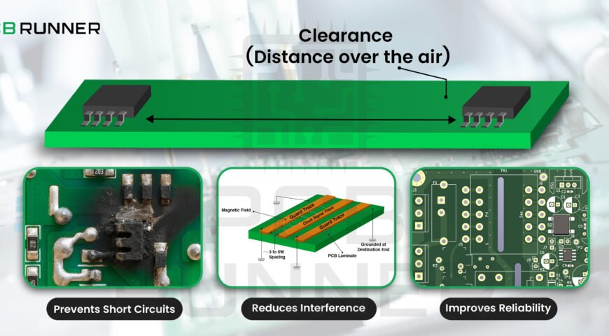
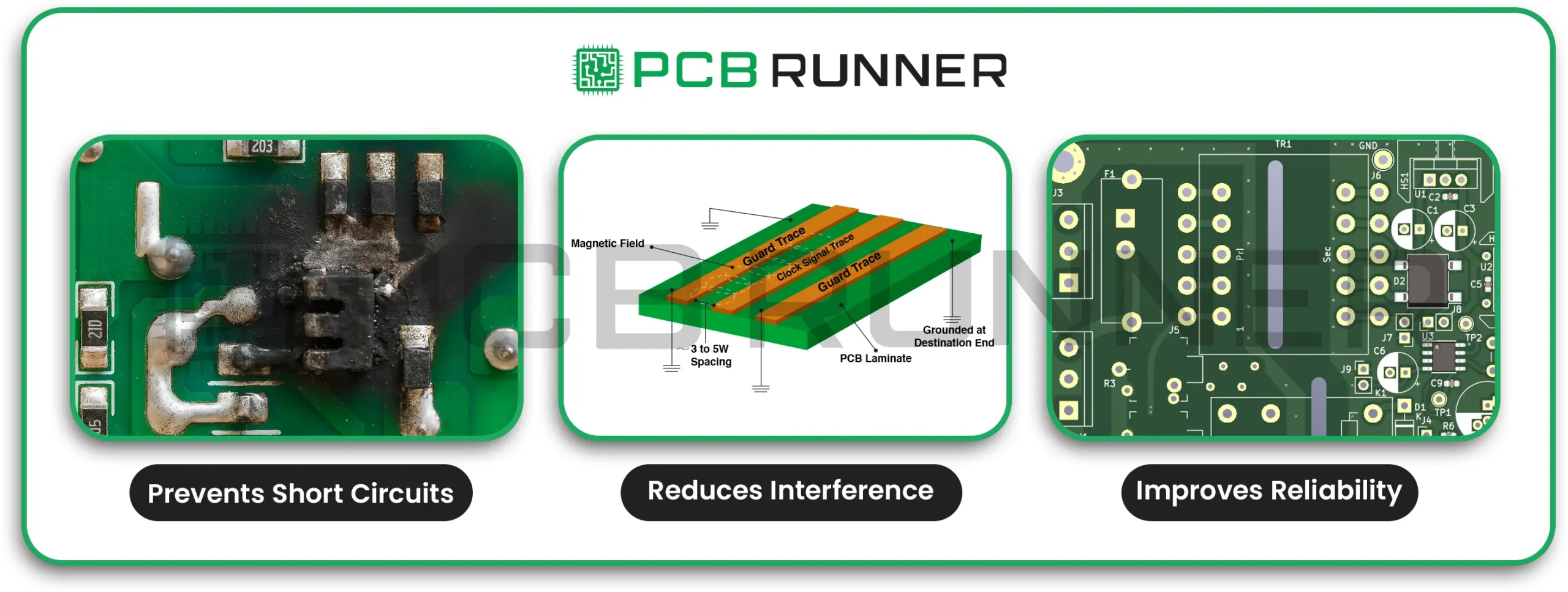
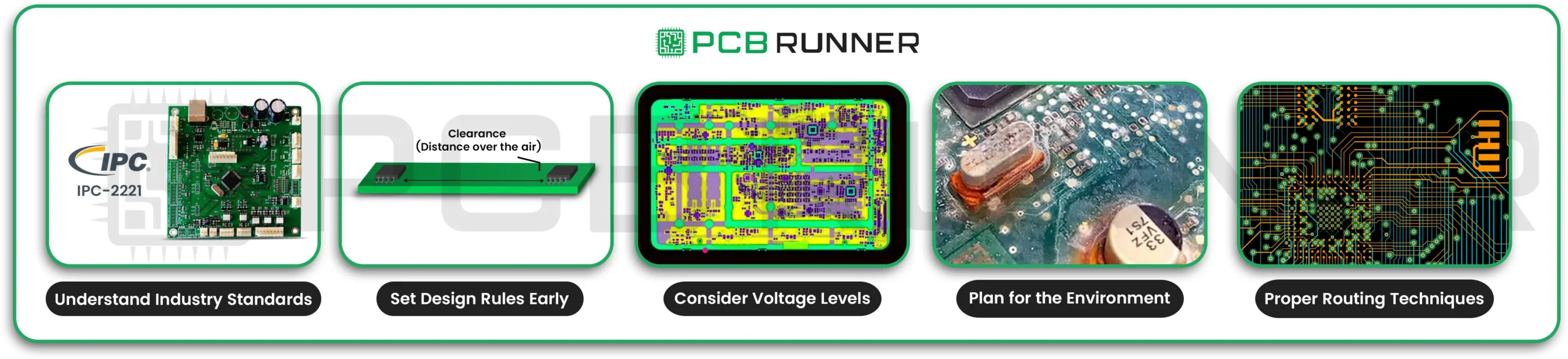
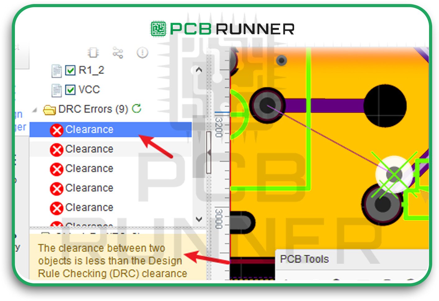
5. Insufficient Clearances

If traces, pads, or components are too close together, you risk short circuits, noise, or even manufacturing errors.

How to avoid it:

  • Follow standard clearance guidelines for your board assembly.
  • Use your design software’s clearance check tools.
  • Don’t try to squeeze too many parts into a small space; leave room for safe connections.

Incomplete or Incorrect Design Data

6. Incorrect Pad Sizes and Spacing

Pads that are too small can make weak solder joints. Pads that are too large can cause components to shift out of place during soldering.

How to avoid it:

  • Use recommended pad sizes for each component type.
  • Keep pad spacing within the limits set by your PCB assembly company.
  • Test your design with a PCB prototype before full production.

Incorrect Pad Sizes and Spacing

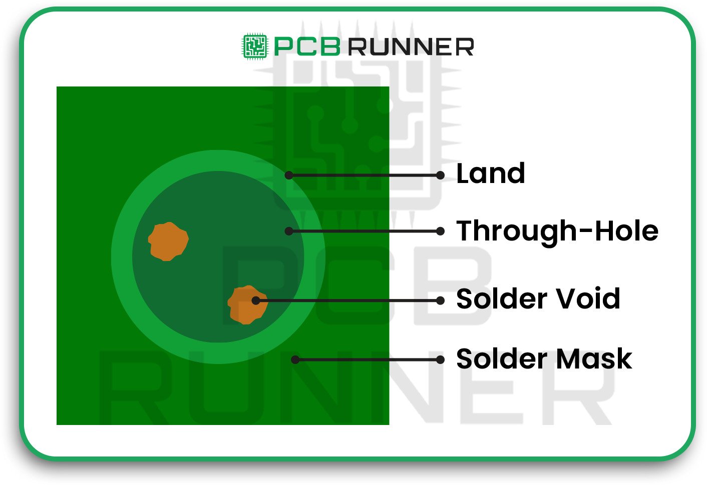
7. Solder Mask Errors

A solder mask keeps solder where it belongs. If the mask openings are incorrect, you may encounter solder bridges or exposed copper that can corrode over time.

How to avoid it:

  • Ensure there’s sufficient space between mask openings and nearby pads or vias.
  • Check for solder mask slivers, which can wash away during manufacturing.
  • Review your design for proper solder mask coverage before sending it to PCB Assembly UK.

Solder Mask Errors

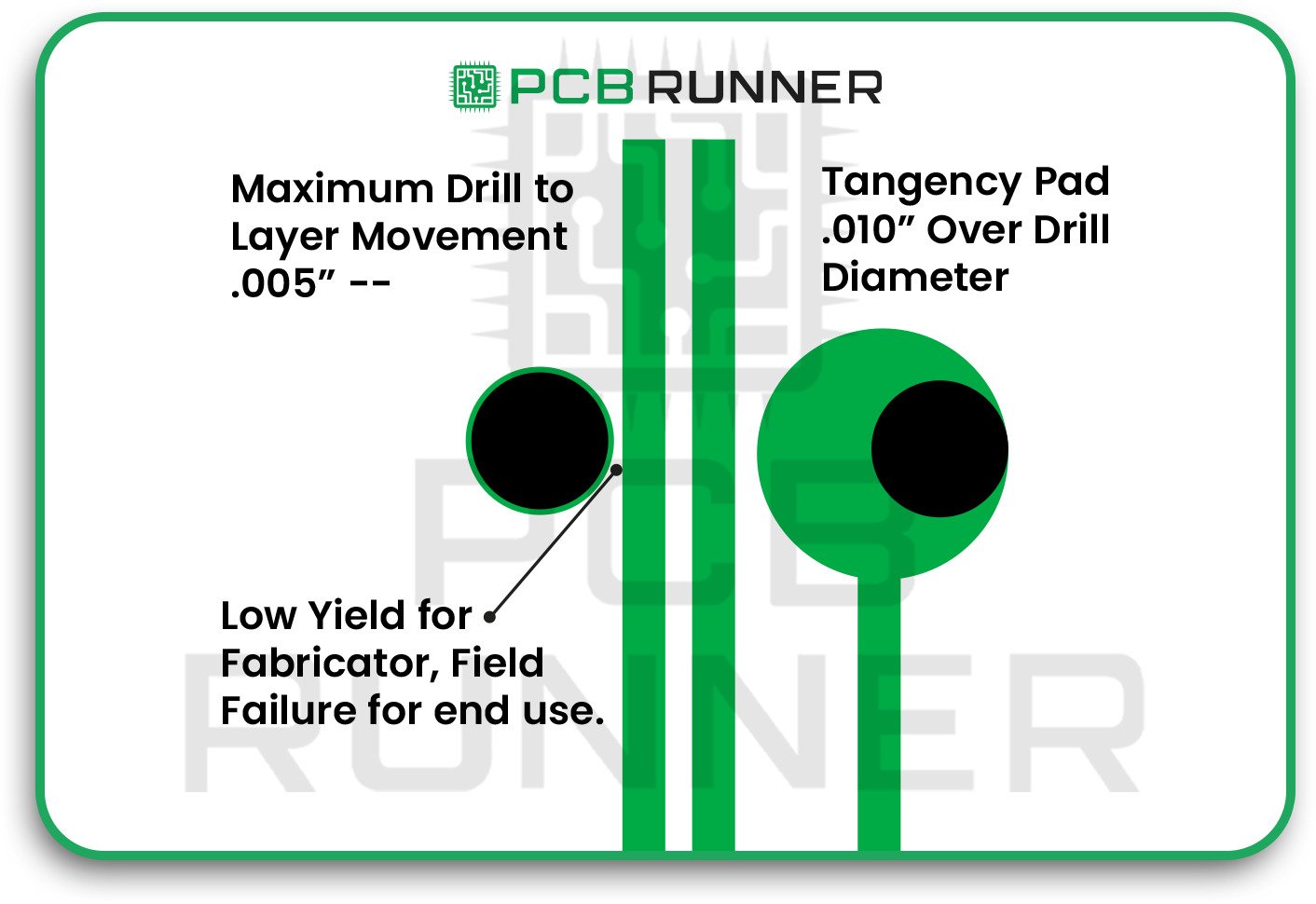
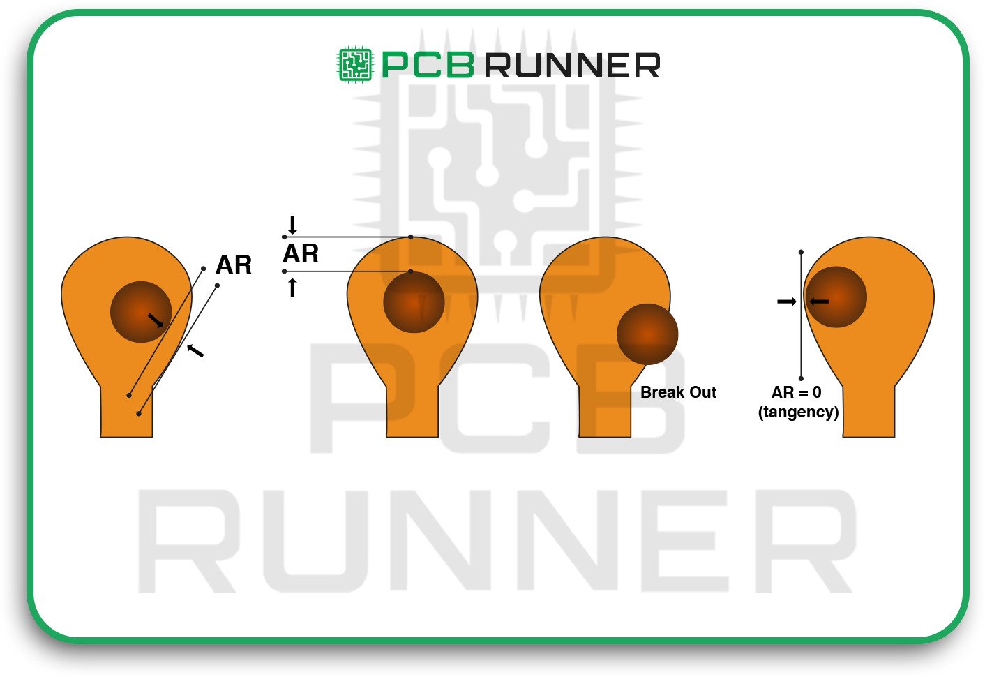
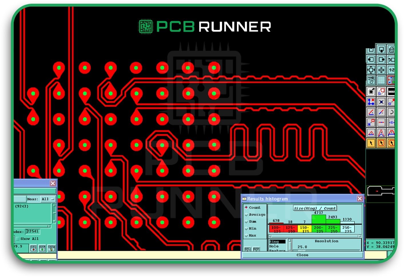
8. Drilling and Annular Ring Problems

Drilling holes for vias or component leads is a delicate process. If the holes are off or the annular ring (the copper around the hole) is too small, you can lose electrical connections.

How to avoid it:

  • Follow your PCB and assembly supplier’s guidelines for hole size, ring width, and spacing.
  • Avoid making holes too close to the edge of the board.
  • Check your finished boards for missing or broken rings.

Drilling and Annular Ring Problems

9. Silkscreen Mistakes

The silkscreen layer indicates the location and orientation of parts. If it’s missing or wrong, your assembly team might make mistakes.

How to avoid it:

  • Ensure that all essential markings (such as polarity or pin 1) are clear and easy to read.
  • Double-check that the silkscreen data matches your assembly instructions.
  • Use high-contrast colours for easy visibility.

Silkscreen Mistakes

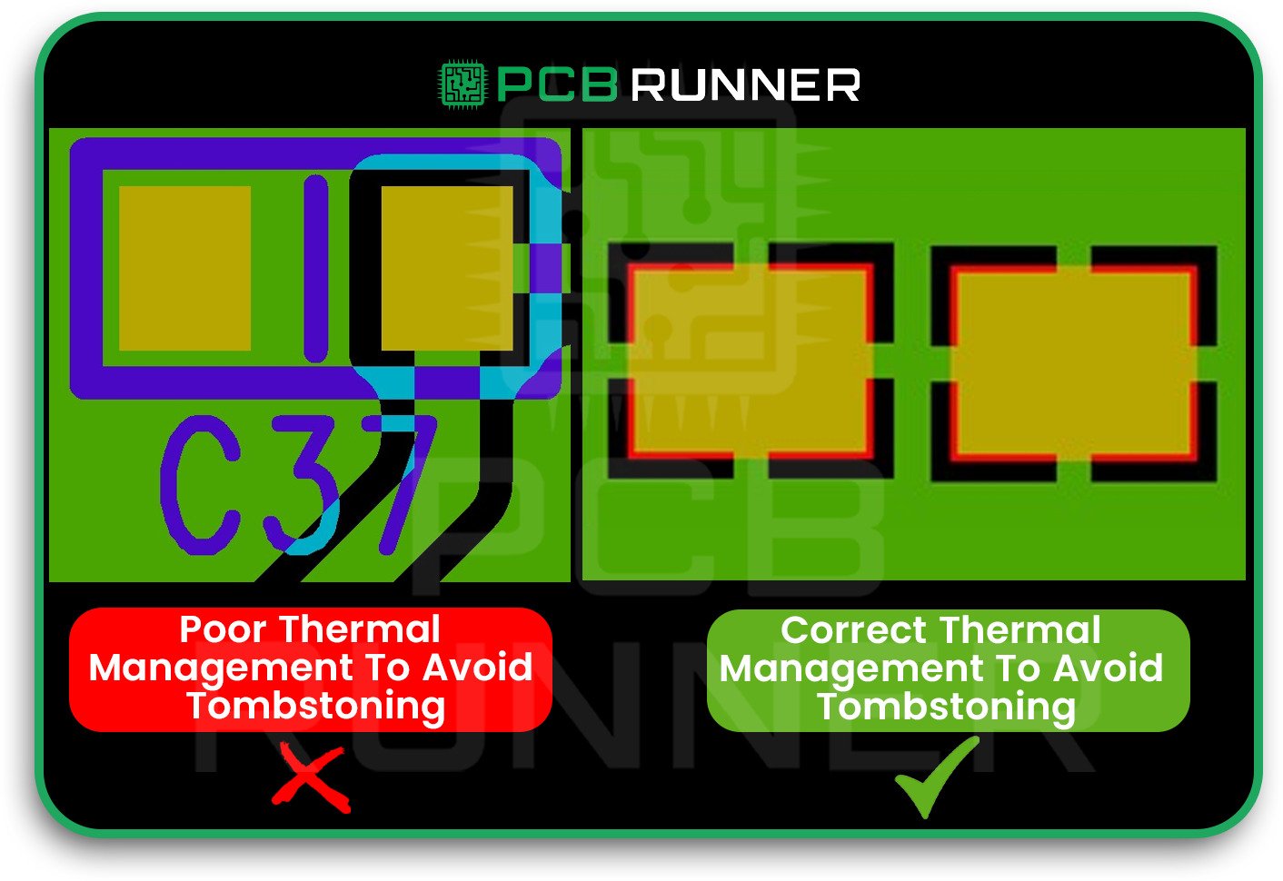
10. Poor Thermal Management

Excessive heat during soldering can damage your board or components. Not enough heat can lead to weak joints.

How to avoid it:

  • Use thermal pads or heat sinks where needed.
  • Control soldering temperatures carefully.
  • Follow DFM (Design for Manufacturability) and DFA (Design for Assembly) guidelines to predict and prevent heat-related issues before assembly.

Poor Thermal Management

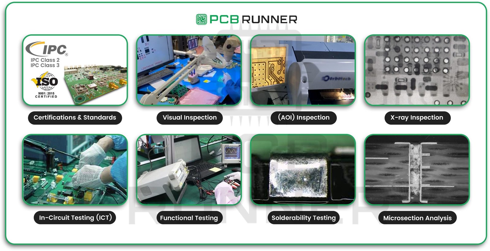
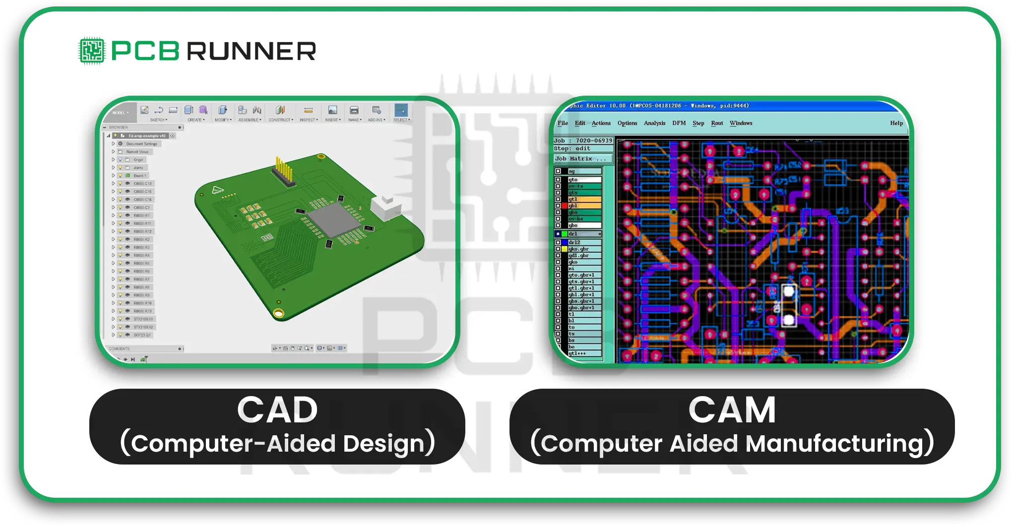
11. Skipping Design for Manufacturability (DFM) Checks

DFM checks help identify problems before your board enters production. Failing to perform these checks can result in costly mistakes and delays.

How to avoid it:

  • Always run DFM checks before sending your design to a PCB assembly company.
  • Utilise online tools or consult with your PCB assembly partner in the UK for assistance.
  • Fix any issues found during the check, even small ones can cause significant problems later.

DFM Checks

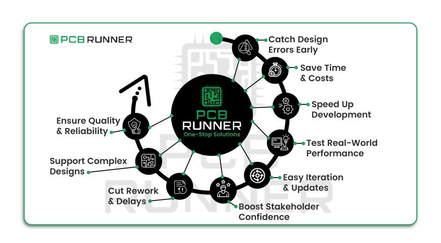
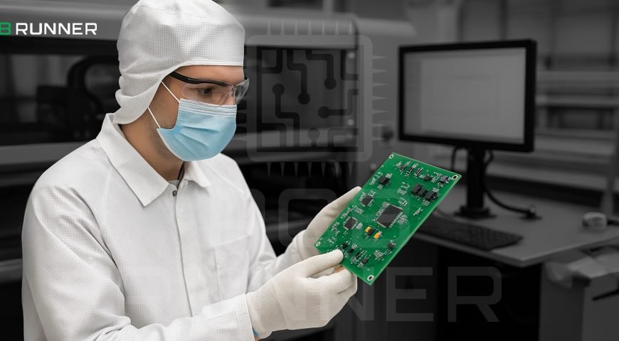
12. Not Testing Prototypes

Jumping straight to mass production without testing a PCB prototype can lead to disaster. Small mistakes can turn into significant losses if you don’t catch them early.

How to avoid it:

  • Build and test a prototype before full production.
  • Use your prototype to identify and correct assembly errors, design flaws, and any issues with real-world performance.
  • Make changes based on your test results before ordering more boards.

Product Highlights: What Makes a Good PCB Assembly Process?

A great PCB fabrication assembly process is:

  • Careful: Every step is checked and double-checked.
  • Clear: All instructions and drawings are easy to understand.
  • Flexible: Mistakes are identified and corrected promptly.
  • Supported: Your PCB assembly company provides assistance and guidance when you need it.

Tips for Different Types of Projects

For simple boards:

Start with a PCB prototype to catch easy-to-miss mistakes.

For complex boards:

Work closely with your PCB assembly company to ensure every detail is correct.

For high-volume orders:

Utilise automated inspection and testing to maintain high-quality standards.

Final Thoughts

PCB assembly doesn’t have to be stressful. By watching out for these common mistakes and following simple steps, you can consistently build better boards. Take your time, review your work, and always test before scaling up. Your next circuit board assembly will thank you for it.

Key Applications and Advantages of Flex Circuits

Key Applications and Advantages of Flex Circuits

Flexible circuits, also known as flex PCBs, are transforming the way we develop and manufacture electronics. Unlike regular circuit boards, these boards can bend, twist, and fit into spaces that standard circuit boards cannot accommodate. If you are wondering why new gadgets are becoming smaller, lighter, and more reliable, flex circuits are a significant contributor to this trend.

In this blog, we will talk about what makes flex circuits special, their uses, and the reasons why more engineers and companies are opting for them. We will also examine how flex PCB suppliers and circuit board suppliers in the UK are contributing to the feasibility of these designs, as well as the importance of selecting the right partners for these companies.  

What Is a Flex Circuit?  

Flexible circuits, also known as flex circuits, are bendable, thin boards that connect electronic parts. Unlike a regular circuit board, which is stiff, a flex circuit can bend and fold without breaking. This enables them to fit in small spaces and for components with moving parts.

Flex circuits utilise specific types of plastic film and thin copper, which enable them to be lightweight, strong, and capable of withstanding heat and vibration more effectively than rigid boards.

What Is a Flex Circuit

Essential Uses of Flex Circuits  

1. Consumer Electronics  

Check out your smartphone, tablet, or laptop. A flexible PCB board is inside, connecting the various components, including buttons, screens, cameras, and batteries. Flex circuits enable slimmer and lighter devices that are packed with features.  

Wearables, such as smartwatches and fitness bands, utilise flex PCBs to ensure a form-fitting, flexible design around the wrist while providing ease of motion.  

Cameras: Small space flexible circuits connect moving lenses with sensors.  

2. Automotive Industry  

Today’s cars are equipped with a wealth of electronics. Flex circuits are incorporated in displays and even used in car lights. In comparison to traditional boards, flex circuits have better handling of vibrations, heat, and tight spaces.  

Dashboards and controls: Flex PCBs connect buttons, screens, and lights.  

  • Sensors: Used in airbags, in seat comfort sensors, and cameras.  
  • Lighting: Modern car lights are slim and flexible circuits that shape to fit them.  

3. Medical Devices  

  • Medical tools require them to be compact, lightweight, and dependable. Flex circuits are ideal for these requirements.  
  • Pacemakers and hearing aids: Flex circuits enable these devices to be implanted within the body and withstand movement.  
  • Diagnostic equipment: Found in portable monitors and imaging devices.

4. Aerospace and Satellites  

  • Space travellers understand that weight matters significantly in space. Fuel and space are both saved by flex circuits compared to rigid boards.
  • Satellites: Flex PCBs withstand vibration and temperature fluctuations during launch and in orbit.  
  • Aircraft: In control panels, sensors and communication systems.  

5. Industrial Equipment  

In regions such as factories, machines can vibrate, move, and generate excessive heat. That allows the use of flex circuits in robots, sensors, and control panels.

Essential Uses of Flex Circuits_

Advantages of Flexible Printed Circuit Boards

1. Space and Weight Savings  

  • Flex circuits are compact structures. They also decrease the space of the end product.  
  • Devices become lighter and more compact.  
  • Reduced bulk also means reduced shipping and handling costs.  

2. Flexibility and 3D Design  

  • Almost any shape can be bent and folded into a new one. This is great for products with odd shapes or moving parts.  
  • Perfect among wearables, foldable phones, and small gadgets.  
  • It can wrap around corners or fit in tight spaces.  

3. Durability and Reliability  

  • Flex circuits endure vibration, bending, and movement better than rigid boards.  
  • Fewer solder joints and connectors result in fewer breakages.
  • Ideal for items that travel or are used in harsh settings.

4. Improved Heat Dissipation

Often more effective than many rigid boards, flex circuits dissipate heat better. This is crucial for maintaining device temperature, which in turn helps them last longer.

5. Decreased Assembly Errors

With fewer connections to manually make because bundles of wires are replaced with flex circuits, there are fewer connections due to fewer manual steps needed. This helps reduce errors during assembly or testing.

6. More Cost-Efficient Over Time

While the initial design of flex circuits may consume more time and money, they often prove to be more cost-effective in the long run. Their design eliminates the need for excess connectors, cables, and additional assembly steps.

In some situations, it can reduce wire costs up to 70 per cent.

Rigid-Flex Boards: The Best of Both Worlds

When a portion of the board needs to be stiff while other portions require flexibility, rigid-flex boards are a helpful solution. Such boards integrate both rigid and flexible sections into one board.

  • It can be found in phones, cameras, and various types of military equipment.
  • Provides complex shapes and reliable interconnections. 

How Flex PCB Design Changes Everything

Fulfilling all benefits revolves around good flex PCB design, so their considerations include: board size, movements involved, and temperature or chemical changes.

How to Maintain Distance Between Signal Paths Short and Clear

Flex PCB suppliers with experience should alleviate your design concerns.

Flex PCB Assembly: Unique Skills Required

  • Every step of a flex PCB assembly differs from typical boards. The materials are more delicate, and regular handling will damage them. 
  • Special machines prevent components from bending or tearing the board during placement and soldering.  
  • Routine quality checks guarantee every board meets performance standards.
  • Having reliable circuit board suppliers in the UK or other locations enhances the accuracy of your assembly. 

Applications of Flex Circuits

  • Smartphones: The screen, battery, and camera are connected with flex circuits.
  • Automobiles: Used in the steering wheel, dashboard, and even the seat sensors.
  • Medical equipment, such as pacemakers and hearing aids, relies on flex circuits for comfort and reliability. 
  • Satellites: Flex circuits save a significant amount of weight while enduring the stress of launching into space and orbiting. 

Things to Keep in Mind When Using Flex Circuits

Trustworthy suppliers: Collaborate with flexible PCB suppliers who possess expertise in your field of work. 

  • Consider movement: If your board is designed to flex and bend frequently, incorporate features that make it more resilient to these movements. 
  • Proxy test first: Before diving into full-scale production, build a prototype to identify and address any potential problems.
  • Assembly considerations: Ensure that your assembly team is briefed on your strategy for the boards.
  • Use rigid-flex if needed: For extra support or intricate shapes, consider using a rigid-flex board for added strength and flexibility.

Challenges to Look Out For

  • Cost: Initially, designing and manufacturing flex circuits can significantly increase spending.
  • Handling: They are skinny and fragile.
  • Guidelines: Flex circuits have special requirements. Always adhere to your supplier’s guidelines.

Partnering with PCB Runner: Why Work with Them for Flex Circuits?

With flex circuits, modern electronics have unprecedented potential. They streamline products, making them lighter, smaller, and more dependable. The benefits are evident across the spectrum, from smartphones and automobiles to medical devices and even satellites, engineers gain refined design capabilities, reduced errors, and enhanced creative freedom.

However, to fully realise the advantages of flexible printed circuit boards, a suitable partnership is crucial. From flex PCB design and prototyping through full flex PCB assembly, PCB Runner has unparalleled experience and expertise. Their dedicated team provides custom support to the unique requirements of flexible circuits, ensuring seamless collaboration and project success.

When you select PCB Runner, you gain more than just a supplier. You are gaining a partner who looks out for your business outcomes, assists you in troubleshooting, and ensures your flex circuits are built to last. That’s how good ideas become great products.

chart

Top Reasons to Use Prototyping in LED Board

When you flip a switch and your LED lamp glows, you probably don’t think about the tiny circuit board inside. But for engineers and makers, the journey from idea to a working LED light PCB board is full of questions and challenges. How do you know your design will work? What if something goes wrong? This is where prototyping comes in. Building a PCB prototype can save you time, money, and stress, especially for projects like an LED PCB board or any new electronic device.

Let’s walk through the top reasons why using prototyping in PCB design is not just smart, but essential. Whether you’re working with PCB manufacturing companies or building your own LED PCB, these insights will help you get it right the first time.

What Is PCB Prototyping?

A PCB prototype is a test version of your circuit board. It’s not the final product, but a working sample you can touch, test, and tweak. Think of it as a rough draft for your electronics project. For tasks like designing LED light circuit boards or developing new gadgets, prototyping helps you identify problems before they become major headaches.

What Is PCB Prototyping

1. Catching Design Mistakes Early

No one gets it perfect on the first try. Even the best engineers make mistakes. By creating a PCB prototype, you can:

  • Test your design in real life
  • Find wiring errors or missing parts
  • Check if your LED lights PCB board glows as expected

Catching mistakes early means you avoid costly problems later. Imagine building 1,000 LED PCB boards, only to find out they don’t work. Prototyping saves you from that nightmare.

2. Saving Money in the Long Run

Some people think skipping prototyping will save money. But it’s the opposite. Fixing problems after mass production is expensive. With a PCB prototype, you:

  • Spend a little now to save a lot later
  • Avoid wasting materials on faulty boards
  • Make changes before you commit to a big order

PCB manufacturing companies know that a small investment in prototyping can prevent huge losses down the road.

3. Speeding Up Your Design Process

It might seem like prototyping adds extra steps. In reality, it speeds up the entire process. Here’s why:

  • You test and fix problems as you go
  • You don’t waste time waiting for a big batch to arrive
  • You can show your team or customers a real, working board

For LED PCB manufacturer teams, quick feedback means quicker progress. You can move from idea to finished product much faster.

4. Testing Real-World Performance

A design that looks good on paper might fail in real life. With a PCB prototype, you can:

  • Check if your LED PCB gets too hot
  • See how it handles power surges or drops
  • Test the brightness and colour of your LED lights

This is especially important for LED PCB assembly. You want to ensure your board works properly in its final application, whether that’s a lamp, sign, or gadget.

5. Making Changes and Improvements

Prototyping gives you freedom to experiment. You can:

Each new prototype brings you closer to the perfect design. You’re not locked in, you can keep improving until you’re happy with the result.

6. Building Confidence with Stakeholders

If you’re working with a team, boss, or customer, showing a real LED PCB board build helps establish trust. A prototype isn’t just a drawing or idea, it’s something you can hold and test. This helps:

  • Get feedback from others
  • Show investors or clients your progress
  • Prove your design works before spending more money

A working prototype is often the key to getting approval for full production.

7. Reducing Rework and Delays

Mistakes found late in the process can cause significant delays. By using a PCB prototype:

  • You spot and fix issues early
  • You avoid having to redo large batches
  • Your project stays on schedule

For PCB manufacturing companies, this means happier customers and fewer complaints.

8. Supporting Custom and Complex Designs

Some projects, such as custom LED displays or smart gadgets, require specialised layouts. Prototyping lets you:

  • Test unique shapes or sizes
  • Try out new features or sensors
  • Make sure your LED PCB fits perfectly in your product

This is much easier (and cheaper) to do with a prototype than with a full production run.

9. Improving Quality and Reliability

Every product should be safe and reliable. With prototyping, you can:

  • Test for overheating or short circuits
  • Check if your LED PCB assembly meets safety standards
  • Make sure your board lasts as long as it should

Quality matters, especially if your product will be used every day or in harsh conditions.

10. One-Stop Solutions from PCB Manufacturing Companies

Many PCB manufacturing companies now offer fast prototyping services. This means you can:

  • Get your prototype made quickly
  • Work with experts who know the latest trends
  • Use high-quality materials and tools

A reputable LED PCB manufacturer can guide you through the entire process, from the initial idea to the finished board.

Tips for Prototyping Success

  • Start simple: Don’t try to do everything at once. Test basic functions first.
  • Take notes: Write down what works and what doesn’t.
  • Ask for help: Good LED PCB manufacturer teams are happy to answer questions.
  • Test in real conditions: Use your prototype the way it will be used in real life.
  • Keep improving: Don’t stop at the first working board. Look for ways to make it even better.

Final Thoughts

Prototyping isn’t just for big companies or fancy gadgets. It’s a smart step for anyone designing a new LED PCB board, lamp, or electronic device. By building and testing a PCB prototype, you save money, avoid mistakes, and end up with a better product.

So next time you have an idea for a new LED light or gadget, remember: start with a prototype. It’s your best tool for turning ideas into reality, one board at a time.

Prototyping is the secret ingredient behind every great LED project. It helps you learn, improve, and succeed, no matter how big or small your idea is.

PCB Assembly

PCB Assembly: How to Evaluate Quality and Reliability

When you pick up a device, your phone, a remote, or even a washing machine, there’s a printed circuit board (PCB) inside, quietly making everything work. But have you ever wondered how these boards are made to last? Or how can you trust that a PCB will work right, every time? The answer lies in quality and reliability, especially during the PCB manufacturing and assembly process.

Let’s take a closer look at what makes a good PCB, how PCB assembly manufacturers test for quality, and what steps you can take to ensure your project is built to last.

Why Quality and Reliability Matter in PCB Assembly

A PCB is like the backbone of any electronic device. If it fails, the whole device can stop working. That’s why PCB production and assembly aren’t just about putting parts together. They’re about making sure every board works as it should, for as long as.

Poor-quality PCBs can cause:

  • Sudden device failures
  • Safety problems
  • Expensive repairs or recalls
  • Unhappy customers

So, when you’re choosing a PCB assembly manufacturer or looking for PCB manufacturing services in the UK, it’s smart to ask: How do they ensure quality? How do they make sure every board is reliable?

Quality and Reliability Matter in PCB Assembly

Key Factors in Evaluating PCB Quality

Let’s break down what to look for when checking the quality of PCB fabrication and assembly:

1. Certifications and Standards

A reputable manufacturer will adhere to industry standards. For example, ISO 9001 certification and IPC Class 2, 3, or 3A qualifications demonstrate that a company adheres to stringent quality standards. These certifications indicate that the manufacturer thoroughly checks every step, from the selection of materials to the production of finished boards.

2. Visual Inspection

This is the first line of defence. Trained staff or machines look for:

  • Misplaced or missing components
  • Soldering problems
  • Scratches or cracks
  • Bent or broken pins

It might seem simple, but catching visible problems early can save a lot of trouble later.

3. Automated Optical Inspection (AOI)

AOI uses cameras and software to scan the board. It compares each board to a “golden” reference board, spotting things like:

  • Wrong parts
  • Soldering defects
  • Misaligned pieces

AOI is fast and accurate, and it’s used at several points during PCB assembly services to catch mistakes before they become bigger issues.

4. X-ray Inspection (AXI)

Some parts, such as Ball Grid Arrays (BGAs), have solder joints that are hidden underneath. X-ray inspection looks inside the board to find hidden problems, such as:

  • Bad solder joints
  • Voids or gaps
  • Short circuits

AXI is especially important for complex boards or those used in safety-critical devices.

5. In-Circuit Testing (ICT)

ICT checks each component on the board. It measures things like resistance, capacitance, and voltage to make sure every part is in the right place and working as it should. If something is wrong, it’s easier to fix at this stage than after the board is fully built.

6. Functional Testing

This is like a “dress rehearsal” for your board. The manufacturer powers up the board and runs it through its paces, just like it would work in real life. If the board passes, you know it’s ready for action. If not, it goes back for repairs.

7. Solderability Testing

Solderability tests check if the pads and component leads can form strong, reliable solder joints. This helps prevent cold joints or weak connections that could fail later.

8. Microsection Analysis

This is a comprehensive examination of the board’s structure. A small piece of the board is cut out and examined under a microscope. This helps identify problems within the board, such as poor plating or delamination, that are not visible from the outside.

Key Factors in Evaluating PCB Quality

What Makes a Reliable PCB Assembly Manufacturer?

A reliable PCB and assembly partner does more than just build boards. They help you avoid problems before they start. Here’s what to look for:

  • Experience: Do they work with industries like medical, aerospace, or defence, where reliability is critical?
  • Transparency: Do they share their testing and inspection processes with you?
  • Support: Can you reach them easily if you have questions or need help?
  • After-sales service: Will they assist you in resolving issues after delivery?

Manufacturers, with their facilities (not just brokers), can usually offer more consistent quality and better support.

How PCB Manufacturing UK Services Ensure Quality

In the UK, top PCB manufacturing and assembly companies employ a combination of manual and automated checks to identify issues early. They review engineering files before starting, offer 24-hour tech support, and provide instant quotes and status updates.

Some even let you upload your design files online for a quick review. This helps catch errors before production starts, saving time and money.

Tips for Evaluating PCB Assembly Quality

  • Ask for test reports: Good manufacturers will share their inspection and test results.
  • Request a sample: Test a few boards before ordering a large batch.
  • Check for certifications: Look for ISO9001 and IPC standards.
  • Visit the factory: If possible, see their process in action.
  • Read reviews: What do other customers say about their reliability?

Product Highlights: Common PCB Testing Methods

Here’s a quick look at the most common tests used in pcb fabrication and assembly:

Test Type What It Checks For When Used
Visual Inspection Obvious defects, missing parts Throughout production
AOI Soldering, placement, alignment Post-assembly
X-ray Inspection (AXI) Hidden solder joints, internal issues For complex boards
ICT Component values, placement After assembly
Functional Testing Real-world operation Final stage
Solderability Testing Solder joint strength Before/after assembly
Microsection Analysis Internal structure, plating For quality audits

Final Thoughts

Quality and reliability in PCB manufacturing and assembly don’t happen by accident. They’re built into every step, from design to final inspection. By understanding the tests and checks used by your PCB assembly manufacturer, you can make smarter choices and avoid costly surprises.

Remember:

  • Always check for industry certifications.
  • Don’t skip inspection and testing.
  • Work with manufacturers who value transparency and support.

A reliable PCB is more than just a collection of parts; it’s the foundation of every great electronic product. Take the time to evaluate quality, and your devices will thank you for it.

Glue Dosing Techniques

Glue Dosing Techniques for High-Quality PCBs

Producing a PCB is similar to constructing a well-built house. Every individual step is essential. One such step is glue application. Glue is used to assist with the friction fit of components during assembly. Like with many processes, using too much or too little can cause problems. This document outlines glue dosing methods for PCBs, addressing the importance of glue, its applications, and how to achieve consistent accuracy.

What is Glue Dosing in PCB Production?

Glue dosing refers to the application of small quantities of adhesive to a PCB board in the course of assembly. The adhesive secures components during the curing and soldering stages. This is useful for small components that are situated at the bottom of the board to prevent them from falling off due to gravity during the soldering stage.

Glue dosing is applicable at various stages of PCB production. This is observed in both PCB prototype work and volume production runs.

What is the purpose of glue in PCB assembly?

  • Maintaining the positional accuracy of the components: Glue prevents components from shifting prior to soldering.
  • Increases assurance: Effective glue application enhances stability and fortifies your PCB printed circuit board assembly.
  • Assistance with custom shapes: Some custom PCB assembly projects involve parts with unusual shapes that require additional support.

purpose of glue in PCB assembly

Glue Category Used in PCBs

Not all glues can be compared. Your requirements determine the type you choose.

  • Epoxy glue: Widely used and potent. Requires heat to cure.
  • Silicone glue: Suitable for parts that move or vibrate, offering pliability.
  • Acrylic Glue: Good for fast jobs and cures quickly.
  • Hot melt glue: Ideal for parts that require heating to melt and cooling to harden.
  • UV curable glue: Cures when exposed to certain light.

Fulfilling different purposes, different types of glue exist. Always verify the part’s datasheet or consult your PCB producer for the proper recommendations.

Glue Category Used in PCBs

How to Prepare Glue Dosing

  • Before anything else, confirm that your PCB boards are free of grit. Glue, especially, won’t adhere to surfaces contaminated with dust, oil, or dirt.
  • Clean with 90% isopropyl alcohol (IPA) solutions.
  • Do not use your bare hands to touch the treated surfaces post cleaning.
  • Allow the surfaces to dry completely before applying the product.

Applying glue will benefit significantly from a well-prepared surface, resulting in a longer-lasting bond.

Glue Dosing Methods

Different techniques can be used to apply glue to a PCB. Your choice of methods will depend on the size of your project and the type of glue you are using.

Manual Dispensing

  • Use a syringe or a small bottle.
  • Best suited for prototypes or small batches.
  • You dictate where the glue goes and in what quantity.

Automated Dispensing

  • These are machines that place glue dots at specific locations.
  • Best suited for massive production runs.
  • Faster than manual work, and more accurate too.

Screen Printing

  • Glue is stuck to the board through a stencil.
  • Best suited for applying glue to multiple areas at once.
  • This is common in some big factories.

Roller Coating and Spraying

  • Glue is either rolled onto the board or sprayed onto it.
  • Best for a large custom board.
  • Most companies prefer automated dispensing because it is fast and accurate.

How Much Glue Should You Use?

This is crucial. Too little glue will allow parts to drop off, while too much will create short circuits in other regions.

  • Use just enough glue to keep the item in position.
  • For most parts, a small dot of glue works best.
  • For larger components, two or more dots may be necessary.
  • Refer to the datasheet for the recommended size and position of the glue.

If you are confused, contact your board manufacturer for advice regarding their default adhesive dot size.

Where to Apply Glue

  • For small chip components, use glue targets that are smaller than the centre of the part.
  • For large chips, dot glue at both ends and on the sides.
  • Avoid placing glue near the part’s leads or pads, as it may block the soldering process.
  • Avoid placing glue on or around test points or connectors.

Effective placement is advantageous for printing the PCB and for the overall assembly.

Curing the Glue

Glue, once applied, needs to be cured or hardened, which is defined as curing.

  • With epoxy glue, the required curing method is heating the glue in an oven.
  • With hot melt glue, it naturally sets as it cools.
  • UV glue requires specific ultraviolet light to cure.
  • Acrylic may require room temperature, heat, or a combination of both to cure.
  • Adhere strictly to the manufacturer’s guidelines on waiting duration and temperature when curing. Uncured components are likely to shift when soldered unless proper measures are taken to prevent them from moving.

QC for Glue Dosing

  • Visually look for glue dots that should be marked as placed and positioned correctly.
  • Check for overflow. Ensure the adhesive is within proper margins and does not extend towards the pads or leads.
  • Confirm that the glue effectively holds the component in place; this is referred to as a bond strength test and should be completed for substantial-sized projects.
  • Some factories have incorporated cameras and automated inspections for monitoring glue dot placement.

If an issue arises, ensure that it is resolved before proceeding to the next step.

Issues from Poor Glue Application

  • Components detached: There was neither sufficient glue nor had it cured.
  • Soldering problems: Pads or leads that are glued could be covered by solder.
  • Short circuits: There may have been too much glue added, which is now spreading and causing shorts.

The most challenging part of the change is that the excess glue can hinder the regular replacement of the parts, making it complicated.

Always strive for the proper amount of glue and its application. Also, ensure that you cure it adequately.

Improvement Techniques for Glue Application

  • Start with less demanding projects before moving to more advanced ones.
  • Maintain consistency by using the same type of glue for each batch.
  • Store adhesive in a cool, dry place to prevent spoilage.
  • Regularly clean your dispensing tools to prevent blockages caused by dirt and debris.
  • Talk to your PCB designer for specific glue dosing instructions.

Glue Application in Custom PCB Assembly

While placing an order for custom PCB assembly, discuss the glue with your supplier. Let them know if your components are heavy, irregular, or need extra support to hold them in place. They can recommend the best glue and the optimal dosing procedure for your specific case.

Safety related to PCB Glue

  • Use a well-ventilated area.
  • Put on gloves, a face shield, and safety goggles.
  • Do not inhale glue vapours.

All steps provided by the glue manufacturer must be followed.

The Importance of Professional Assistance with Dosage PCB Glue

Getting the glue dosing wrong can derail the creating of quality PCB boards. The more correctly glue is applied, the right amount, in the correct location, and at the right time, the better the boards will be in quality. With clean boards, careful placement of glue, and proper curing, you can eliminate issues such as parts coming loose or experiencing soldering problems. Never skip checking your work, following safety protocols, and seeking guidance when necessary.

Having a dependable partner, such as PCB Runner, is helpful when you need advice or professional manufacturing services. PCB Runner is notable for its knowledge and dedication in the area of PCB (Printed Circuit Board) manufacturing and assembly. They guide you from prototype to production, paying attention to details such as glue dosing, assembly, and quality checks. Their team understands that every step is essential and works to ensure your boards are accepted without any rework.

Choosing a knowledgeable partner, such as PCB Runner, ensures that your PCBs will be built with utmost care, adhering to best practices for glue dosing and all other aspects of functionality. This improves the chances of your projects succeeding and ensures your boards function effectively in the world.

PCB Assembler

The Ultimate Checklist for Selecting a PCB Assembler

Selecting a PCB assembler is a crucial decision that impacts the entire project. Correct choices lead to time and cost efficiency, while incorrect decisions can result in hours spent troubleshooting avoidable issues. This blog aims to provide clear, articulated guidance, practical insights, and effective strategies tailored to you.

Why It Matters

Think back to your most recent group assignment. Everyone worked hard, and it almost fell apart because one person did not pull their weight. Choosing a PCB assembler is similar to picking that teammate. You need someone dependable, competent, and someone who does not complicate things further. While building a custom printed circuit board requires skill, it also requires an equally skilled collaborator.

PCB assembler

In Their Skill Set, Do They Have Experience with PCB Prototyping?

The same applies to offering specialised services. A plumber cannot attend to automobile issues. In parallel, ask if they have experience managing similar projects. Have they developed prototype circuit boards for comparable products? Do they understand the distinction between a rushed prototype and an elaborate final offering? If a vendor understands prototype PCB manufacturing, it translates to far less guesswork on your end.

PCB Prototyping

Are They A Full-Service Provider?

Some firms are limiting themselves to an assembly-only approach, while others undertake everything from design and fabrication to assembly and testing. Life becomes easier when dealing with full-service printed circuit board manufacturers in the UK. You do not have to manage multiple vendors. Diagonal communication problems are less likely to occur. Issues are resolved more quickly. You receive a custom-printed circuit board designed specifically for you.

Full-Service Provider

What Certifications And Standards Do They Follow?

Certification and standards are relevant because they demonstrate your company’s commitment to quality. Look for ISO 9001 and IPC-A-610 certifications. These demonstrate that your company values quality processes. If your company is serious about safety, it will also follow RoHS regulations. Do not be shy to ask for verification. A reputable prototype PCB board manufacturer will provide documentation without any problems.

Certifications

How Soon Can They Deliver?

Time is money. When testing ideas, getting results is critical. Are urgent orders accepted? Is rapid PCB prototyping offered? If deadlines cannot be met, continue searching. A reliable assembler understands that sometimes flexibility is a must.

What Kind of Engineering Support Do They Provide?

Assess the nature of communication with the company. Does the support team include an engineer? Do they offer resolution assistance, or do they opt to provide apologies for errors made? During the phases of prototype fabrication, support helps ease troubleshooting within the design. Timely prototype manufacturing support encourages builders to focus more on construction than on worrying.

How Do They Source Components?

Assess the nature of communication with the company. Does the support team include an engineer? Do they offer resolution assistance, or do they opt to provide apologies for errors made? During the phases of prototype fabrication, support helps ease troubleshooting within the design. Timely prototype manufacturing support encourages builders to focus more on construction than on worrying.

What Quality Control Tests Are Performed?

Negligence should never be tolerated, especially when it comes to orders placed to cater to specific needs. Engineers have shamed the profession by designing circuits whose faults may not be eyeballed. Automated Optical Inspection (AOI) cameras have also been collectively linked, albeit unphonically. Automated Optical Inspection (AOI) cameras indiscriminately index their targeted boards and overlook thoroughly tested units with disregard.

Can They Scale with Your Project?

You may begin with ten boards; however, consider the flexibility of scaling up to one hundred orders or even a thousand the following year. Determine if they can handle larger orders as demand increases. A capable prototype PCB board manufacturer should be able to scale production when needed.

What Equipment Do They Use?

Outdated devices may be prone to more errors. Do they have modern pick-and-place machines? Are both surface mount and through-hole parts within their capability range? The proper equipment increases the chances of better boards. Don’t hesitate to request a tour or pictures.

What Do Other Customers Say?

Do they complete orders on schedule? Are the products functioning as specified? If possible, try to talk to someone who has used the service. Actual experiences are much more valuable than brochures filled with flowery language.

Are They Honest and Helpful After the Sale?

Everyone makes mistakes sometimes. Will they help you resolve issues? Good assemblers take responsibility for their work. After paying, most people expect services to disappear, but responsive businesses continue to engage their clients.

What About Pricing?

The cheapest option isn’t always the best option. Ensure that you receive a detailed estimate. What does it cover? Are there additional fees for testing or expedited services? Ensure that all costs are transparent and that there are no hidden fees. A dependable assembler will always provide cost transparency.

Product Highlights: What Sets a Good Assembler Apart

Prompt delivery for PCB prototyping

  • Orders ranging from single pieces to a thousand are welcomed
  • Genuine engineering guidance, beyond just marketing
  • Design, fabrication, assembly, and testing services offered under one roof
  • Backed by quality certifications and customer testimonials

Project guidance tips

  • Prototypes that are simple in design:
  • Opt for flexible order management. Select a vendor that combines agility and reliability in delivery timelines to ensure streamlined order completion.
  • Elaborate custom and complex printed circuit board projects:
  • Focus on thorough, advanced testing, engineering support, and the integration of complex components.
  • Ready for expansion?

Look for scalability in the partner/vendor. Confirm their staffing and equipment capabilities for larger workloads.

Your Success Checklist

  • Do they have a proven track record with similar projects?
  • Are they a single-source supplier?
  • Are they compliant with industry norms?
  • Can they meet milestones?
  • Will real engineering staff provide support?
  • What is their policy regarding parts and sourcing?
  • What are their testing protocols?
  • Can they grow with you?
  • What is their equipment?
  • What do customers report?
  • Are they transparent regarding support and pricing?

Final Remarks

In choosing a PCB assembler, one cannot simply consider price or quick turnaround. It requires a diligent evaluation of a partner that genuinely cares about your success. Use this checklist prior to placing your order. Pose queries. Ensure responses and trust your instincts.

The PCB is the heart of the product. It deserves the best care and attention. It can help transform ideas presented in sketches into working prototypes and could even become the next market sensation.

Have this checklist handy at all times. Never forget, the foundation of every outstanding product starts with a single, precisely engineered prototype. Ensure yours is memorable.

Clearance Strategie

Designing High-Performance PCBs with Optimised Clearance Strategies

Ever wondered why some circuit boards last for years, while others fail in months? The answer often lies in the details, especially in how the board is designed and built. One of the most essential details is clearance. That’s the space between different parts of your PCB. Get it right, and your board works safely and reliably. Get it wrong, and you risk short circuits, noise, or even total failure.

Let’s explore how printed circuit board manufacturers, circuit board suppliers in the UK, and design teams utilise clearance strategies to create high-performance PCBs that stand the test of time.

Why Clearance Matters in Circuit Board Design

Clearance is more than just empty space. It’s a shield, protecting your board from electrical problems, heat, and even physical damage. In circuit board design, clearance means the minimum distance between copper traces, pads, and other conductive elements.

Why is this important?

  • Prevents short circuits: If traces are too close, electricity can jump across and cause a short.
  • Reduces interference: Proper spacing helps avoid signal noise and crosstalk.
  • Improves reliability: Boards with good clearance are less likely to fail, even in harsh environments.

Think of clearance like the lanes on a motorway. If cars (signals) have enough space, traffic flows smoothly. If lanes are too narrow, accidents are more likely to occur.

Clearance Matters

Key Clearance Strategies for High-Performance PCBs

1. Understand Industry Standards

Most PCB board manufacturers follow strict rules set by groups like IPC. For example, IPC-2221 provides guidelines for minimum spacing based on voltage and environmental conditions. Always verify the standards your project requires.

2. Set Design Rules Early

Before you start your PCB layout, set your clearance rules in your design software. This helps avoid mistakes later. Good PCB manufacturing services will review these rules before production begins.

3. Consider Voltage Levels

Higher voltages need more space between conductors. For example, a board handling 1000V needs much bigger gaps than one with 5V signals. This helps prevent arcing and breakdown.

4. Plan for the Environment

Boards exposed to moisture, dust, or chemicals need extra clearance. Contaminants can lower the breakdown voltage, making shorts more likely to occur. Outdoor or industrial boards often need wider gaps than those used in clean offices.

5. Use Proper Routing Techniques

  • Keep traces apart: Space traces generously to avoid crosstalk and interference.
  • Avoid parallel runs: Don’t run high-speed or high-voltage traces side by side for long distances. If you must cross, do it at right angles.
  • Solid ground planes: Use large, continuous ground planes to shield signals and improve stability.

Key Clearance Strategies

The PCB Layout Process: Step by Step

Designing a reliable PCB isn’t just about drawing lines. It’s a careful process that involves planning, checking, and testing at every stage.

Step 1: Define Your Goals

Begin by determining what your board needs to accomplish. Make a list of features, connections, and size limits. Think about where the board will be used. Will it be exposed to high temperatures, vibration, or moisture?

Step 2: Create a Schematic

Draw a detailed circuit diagram. This is your blueprint, showing every part and connection. A clear schematic makes the next steps much easier.

Step 3: Choose Components and Place Them Wisely

Place parts based on their function, heat resistance, and accessibility. Group related parts together. Keep high-power and sensitive parts apart. This makes routing easier and reduces interference.

Step 4: Route Traces with Clearance in Mind

Connect the parts using traces. Follow your clearance rules. Use wider traces for high current. Add extra space around high-voltage areas. If you need to change layers, use multiple vias for heavy currents.

Step 5: Review, Test, and Validate

Check your design for errors. Use your software’s design rule check (DRC) to catch spacing problems. Build a prototype and run tests for continuity, resistance, and capacitance. Fix any issues before moving to mass production.

High-Voltage Clearance: Safety First

If your board handles high voltages, like in electric vehicles or industrial machines, clearance becomes even more critical. Here’s what to keep in mind:

  • Clearance: This is the shortest distance through air between two conductors.
  • Creepage: This is the shortest path along the surface of the board.

Both must be large enough to prevent arcing or breakdown. Always follow industry standards and consult with your PCB fabrication assembly partner if unsure.

Do:

  • Use your design tool’s DRC to enforce spacing rules.
  • Create special “high voltage” zones with extra clearance.
  • Double-check spacing visually and with your manufacturer to ensure accuracy.

Don’t:

  • Rely on default spacing for high-voltage areas.
  • Route high-voltage traces under components that have insufficient space.
  • Ignore the effects of dust, moisture, or ageing on insulation.

Tips for Different Board Types and Applications

Every project is different. Here are some tips for everyday situations:

For consumer electronics:

  • Space is tight, but don’t skimp on clearance.
  • Use ground planes to reduce noise.
  • Keep power and signal traces apart.

For industrial or outdoor boards:

  • Use wider gaps to handle dirt, moisture, and higher voltages.
  • Protect traces with conformal coating if needed.

For high-speed boards:

  • Avoid long parallel traces.
  • Use controlled impedance traces where needed.
  • Keep return paths short and direct.

For multi-layer boards:

  • Use internal layers for power and ground.
  • Stagger the vias to avoid bottlenecks.

Lesson: Always design with the real world in mind, not just the clean lab.

How Circuit Board Suppliers UK Help with Clearance

Good circuit board suppliers in the UK and PCB board manufacturers do more than just build boards. They review your design, check for clearance issues, and suggest improvements. Some even offer after-sales support and quick assistance if you encounter any problems.

Choosing a supplier with experience in your field, whether it’s medical, aerospace, or industrial, means they know the common pitfalls and how to avoid them.

Product Highlights: What to Look for in PCB Manufacturing Services

When choosing a PCB manufacturing services partner, look for:

  • Experience with your application: Medical, automotive, industrial, etc.
  • Clear communication: They should explain their clearance and quality checks.
  • Fast prototyping: Quick turnarounds enable you to test and refine your design.
  • Quality certifications, including ISO 9001 and IPC standards, demonstrate a commitment to quality.

Final Thoughts: Small Gaps, Big Impact

Clearance might seem like a small detail, but it’s one of the most essential parts of circuit board manufacturing. With the right strategies, you can build boards that work reliably, even in harsh conditions. Whether you’re a hobbyist, engineer, or buyer, understanding clearance helps you make better choices and avoid costly mistakes.

So next time you sit down to design a PCB, remember: a little extra space can make all the difference. Give your signals room to breathe, and your board will appreciate it.

Designing high-performance PCBs isn’t just about clever circuits or fancy parts. It’s about getting the basics right, starting with clearance. Keep it simple, keep it safe, and your boards will deliver top performance every time.

Stronger CAD-CAM Data Flow

Improving PCB Efficiency with Stronger CAD-CAM Data Flow

Ever found yourself staring at a tangled mess of circuit lines, wondering if your PCB will actually work? You’re not alone. For many in the electronics world, the journey from idea to finished circuit board can feel a bit like crossing a minefield, one wrong move and you’re back to square one. But what if you could make the process smoother, faster, and less stressful? That’s where a strong CAD-CAM data flow comes in. Let’s explore how this approach can enhance efficiency for everyone involved in PCB fabrication in the UK and beyond.

Why Data Flow Matters in PCB Design

Printed circuit boards (PCBs) are everywhere, from your phone to your fridge. But making them isn’t just about drawing lines and dots. It’s about getting every detail right, from the first sketch to the final assembly. If you’re working with PCB circuit board manufacturers or handling your own PCB printed circuit board assembly, you know how easy it is for things to go wrong.

A strong CAD-CAM data flow bridges the gap between design and manufacturing. It helps you avoid mistakes, save time, and reduce stress. Let’s break it down, step by step.

What is CAD-CAM Data Flow?

  • CAD stands for Computer-Aided Design. This is where you create your circuit board using PCB design software or PCB board design software.
  • CAM is Computer Aided Manufacturing. This is where your design becomes a tangible product.

Data flow refers to the process by which information moves from one stage to the next. If your data flow is weak, you risk errors, delays, and wasted money. If it’s strong, you get a board that works, first time, every time.

Cad & cam pcb design

The Common Fears in PCB Design

Let’s be honest. PCB design can be nerve-wracking. Here are a few worries that keep designers up at night:

  • Did I forget a layer? Missing files can halt production.
  • Are my traces too close? Design rule errors can make the board unusable.
  • Will the manufacturer understand my files? Miscommunication leads to costly mistakes.
  • What if my board fails the testing? Redesigns mean lost time and money.

These fears are real. But with better CAD-CAM data flow, you can put most of them to rest.

Common Fears in PCB Design

How a Strong Data Flow Makes Life Easier

A good data flow is like a well-oiled machine. Every part works together, and nothing gets lost along the way. Here’s how it helps:

  • Clarity: Everyone knows what’s expected.
  • Fewer errors: Problems are caught early, not after the board is made.
  • Speed: Less back-and-forth, so you meet your deadlines.
  • Confidence: You know your design will be built as planned.

Key Steps to Improving CAD-CAM Data Flow

1. Choose the Right Tools

Start with reliable PCB drawing software or PCB design software. These tools help you stick to the rules and catch errors before they become problems. Popular options in the UK include DesignSpark, Altium, and others.

2. Keep Your Files Organised

Give your files clear names. Keep all layers, copper, silkscreen, solder mask, and drill, in one folder. This makes it easy for PCB circuit board manufacturers to find what they need.

3. Check Early, Check Often

Design rule checks (DRC) in your software. This is like spellcheck for your design. It spots problems before you send your files off.

4. Communicate Clearly with Your Manufacturer

Share all your files and notes. If you’re working with PCB fabrication experts in the UK, ask for their preferred file formats. Some companies offer instant quotes and 24-hour support, making it easier to get your questions answered quickly.

5. Use Visual Tools

Many PCB board design software packages let you preview your board in 3D. This helps you spot mistakes before production starts.

6. Review and Revise

Before you hit send, double-check everything. Ask a colleague to review your design. Two sets of eyes are better than one.

Product Highlights: What Makes a Good PCB Design Tool?

When choosing PCB drawing software or PCB board design software, look for:

  • Easy-to-use interface: You shouldn’t need a degree to use it.
  • Built-in checks: Automatic design rule checks save time.
  • File compatibility: Works with the formats your manufacturer needs.
  • 3D previews: See your board before it’s built.
  • Good support: Help when you need it, day or night.

Tips for Different Types of PCB Designers

For beginners:

  • Start simple. Use basic features until you’re comfortable.
  • Don’t be afraid to ask for help. Many manufacturers offer free advice.
  • Watch tutorials. There’s no shame in learning from YouTube.

For experienced designers:

  • Explore advanced features like impedance control and high-speed routing.
  • Customise your libraries for faster design.
  • Share tips with your team to keep everyone up to speed.

For teams:

  • Use cloud storage or secure FTP to share files safely.
  • Hold regular design reviews. Catch mistakes before they become problems.
  • Document your process so new team members can jump in quickly.

Common Pitfalls and How to Avoid Them

  • Incomplete files: Always double-check you’ve included every layer and note.
  • Ignoring manufacturer guidelines: Follow their rules for file formats and design specs.
  • Skipping design checks: Don’t rely on luck. Use your software’s checking tools.
  • Poor communication: If you’re unsure, ask. It’s better to ask twice than get it wrong.

The Role of PCB Manufacturers in Data Flow

Good PCB circuit board manufacturers do more than just make boards. They help you spot problems, answer questions, and guide you through the process. Some even offer design services, enabling you to receive assistance with complex layouts or special requirements.

PCB fabrication UK companies often provide:

  • File reviews: They check your files before production.
  • Quick Quotes: Know Your Costs Upfront.
  • Tech support: Get answers when you need them.
  • After-sales service: Help if something goes wrong.

The Future: Smarter, Faster, Better

As technology improves, so do our tools. Modern PCB design software is becoming increasingly intelligent, with features such as real-time collaboration and automatic error correction. This means fewer mistakes and faster turnaround times.

Stronger CAD-CAM data flow isn’t just a nice-to-have. It’s the key to building better boards, faster, and with less stress.

Final Thoughts

Improving PCB efficiency is all about making life easier for everyone involved. Whether you’re a hobbyist, a student, or a seasoned engineer, a strong CAD-CAM data flow helps you get the job done right. Use good PCB design software, keep your files organised, and communicate clearly with your manufacturer. You’ll save time, avoid headaches, and end up with a board that works, first time, every time.

So, next time you sit down to design a PCB, remember: a little extra care at the start can save you a world of trouble later on. 

Proper Stiffener Selection

Enhancing Flex PCBs with Proper Stiffener Selection

Flexible printed circuit boards, also known as flex PCBs, are revolutionising the way we design electronics. They bend, twist, and fit into places where regular boards can’t go. But this flexibility also brings new challenges. Sometimes, you need certain parts of your flexible PCB board to stay firm. That’s where stiffeners come in.

Choosing the right stiffener for your flex PCB design can make all the difference. It can help your product last longer, withstand more stress, and perform better in challenging conditions. Let’s explore why stiffeners matter, how to pick the right one, and what you should know before you start your next project.

Why Flex PCBs Need Stiffeners

Think of a flex PCB like a piece of paper. It bends easily, which is great for fitting into tight spaces. However, if you attempt to attach a heavy sticker or connector to it, the paper will sag or tear. The same thing can happen to a flexible printed circuit board. That’s why flex PCB suppliers and designers use stiffeners; they give support where it’s needed most.

Key Benefits of Stiffeners

  • Reduce bending stress: Stiffeners prevent the board from bending excessively in specific areas.
  • Support heavy parts: They create a solid base for connectors, chips, and other components.
  • Help with assembly: Stiff areas make it easier for machines to pick and place parts during flex PCB assembly.
  • Protect solder joints: Less flex means less chance of cracked or broken connections.
  • Improve heat handling: Metal stiffeners can help move heat away from hot spots.

Key-Benefits-of-Stiffeners

Where Are Stiffeners Used in Flexible Printed Circuit Boards (Flex PCBs)?

Not every part of a flexible PCB board needs to be stiff. Stiffeners are usually added to:

  • Connector areas: Where cables or plugs attach.
  • Component zones: Under heavy or sensitive chips.
  • Mounting points: Where screws or bolts hold the board in place.
  • ZIF connectors: To meet the thickness requirements for special connectors.

Adding stiffeners only where needed keeps your board light and flexible everywhere else.

Types of Stiffener Materials

Different jobs call for different materials. Here are the most common stiffener types used by circuit board suppliers uk and rigid flex pcb manufacturer teams:

Stiffener Type Main Features Typical Uses
Polyimide (PI) Light, flexible, heat-resistant Moderate support, easy bending
FR4 Rigid, same as standard PCB material Strong support, component mounting
Aluminum Very rigid, great for heat dissipation High-power, heat-prone areas
Stainless Steel Strong, resists bending and heat High-strength, harsh environments
Plastic Lightweight, not as strong as others Low-stress, cost-sensitive areas

Polyimide stiffeners are ideal when you need support but still require flexibility. FR4 stiffeners are commonly used to create a flat, solid area for parts and connectors. Aluminium and stainless steel are best suited when you need to transfer heat or handle large forces.

How Thick Should Your Stiffener Be?

Stiffener thickness depends on the job. Here’s a quick guide:

  • 0.2mm to 0.5mm: For light support or small connectors.
  • 0.8mm to 1.6mm: For heavier parts or where more strength is needed.
  • 2.0mm or more: For very demanding jobs, like large connectors or mounting points.

Always match the stiffener thickness to your board’s needs. Too thin, and it won’t help. Too thick, and you may lose flexibility or make assembly more difficult.

How Stiffeners Are Attached

There are a few ways to add stiffeners to a flexible printed circuit board:

  • Adhesive bonding: Glue holds the stiffener in place.
  • Lamination: The stiffener is pressed and heated onto the board.
  • Mechanical fastening: Screws or clips hold the stiffener (less common).

Most flex PCB suppliers use adhesive or lamination because it’s fast and reliable.

How Stiffeners Are Attached

Design Tips for Using Stiffeners

When planning your flex PCB design, keep these tips in mind:

  • Overlap coverlay: Ensure the stiffener overlaps the coverlay (the flexible solder mask) by approximately 0.75 mm. This spreads out stress and keeps the board firm.
  • Maintain even thickness: If you use more than one stiffener, try to maintain a uniform thickness.
  • Place stiffeners on the same side as the parts: This makes assembly easier and facilitates soldering.
  • Consider heat: Use metal stiffeners if your board becomes too hot.
  • Double up for extra strength: For boards that face bending in both directions, add stiffeners to both sides.

Real-World Example: Wearable Tech

Imagine you’re designing a fitness tracker. The board needs to wrap around a wrist, but it also needs a solid spot for the charging port and battery. By adding an FR4 stiffener under the connector, you ensure it stays in place, even after hundreds of charges. The rest of the board remains thin and bendy, making it comfortable to wear.

Common Mistakes to Avoid

  • Adding stiffeners everywhere: This makes your board heavy and stiff, losing the benefits of a flexible PCB board.
  • Using the wrong material: Avoid using plastic where heat resistance or strength is required.
  • Ignoring thickness: Using materials that are too thick or too thin can cause problems during assembly or use.
  • Not talking to your supplier: Always check with your flex PCB suppliers or circuit board suppliers UK before finalising your design.

Product Highlights: What Makes a Good Stiffener Choice?

A good stiffener:

  • Matches the needs of your design (strength, heat, flexibility)
  • It is placed only where needed.
  • Uses the right thickness for the job
  • Is attached securely and evenly

Rigid-flex PCB manufacturers often assist in selecting the optimal stiffener for your project. Don’t be afraid to ask for advice.

Tips for Different Types of Flex PCB Assembly

For lightweight wearables:

  • Use polyimide stiffeners for gentle support that won’t add bulk.

For industrial or automotive boards:

  • Pick FR4 or metal stiffeners to handle vibration, heat, and heavy use.

For medical devices:

  • Select materials that are safe and reliable, and ensure that stiffeners are only used where necessary to maintain comfort and stability.

Final Thoughts

Stiffeners might seem like a small detail, but they can make or break your flexible printed circuit board. The right stiffener keeps your board strong where it matters and flexible everywhere else. It helps your product last longer, work better, and handle the real world.

So, next time you start a flex PCB design, remember to think about stiffeners. Contact your flex PCB suppliers or circuit board suppliers in the UK as early in the process as possible. Test different options if you can. And always match your stiffener choice to your project’s needs.

A smart stiffener strategy is the key to maximising the benefits of your flex PCB assembly, no matter what you’re building.

PCB-Driven Innovation as a Catalyst for Scaling Defence Sector Business

PCB-Driven Innovation as a Catalyst for Scaling Defence Sector Business

The defence sector in the UK and Europe is moving at a rapid pace. As threats change and technology advances, so does the need for smarter, more reliable systems. At the heart of this progress is the humble printed circuit board (PCB). Today, PCBs are not just the backbone of electronics, they are the driving force behind innovation, helping defence businesses scale and succeed.

Why PCBs Matter in Defence

Every modern defence device, from radar systems to unmanned drones, relies on PCBs. Without them, there would be no signal processing, power management, or secure communications. The demands in defence are challenging: PCBs must survive heat, moisture, shock, and even radiation. They must also meet strict standards for quality and security because failure is not an option in the field.

PCB Production UK: Supporting Local Defence Growth

For defence companies in the UK, working with local PCB production partners offers significant advantages. Quick turnaround, easier communication, and compliance with UK and EU defence standards are just the start. PCB production UK facilities are set up to handle everything from rapid prototyping to full-scale manufacturing, giving your business the flexibility to move fast and scale up when needed.

Meeting Defence Standards: Why It’s Critical

Defence PCBs are held to some of the highest standards in the world. They must meet military specifications like MIL-PRF-31032 for design and manufacturing and IPC-6012/6013 for performance and reliability. These standards ensure that your boards will work in the toughest environments, whether in a submarine, a jet fighter, or a satellite.

Key Defence Standards for PCB Manufacture

MIL-PRF-31032: General military PCB requirements

MIL-PRF-55110: Rigid PCB requirements

MIL-PRF-50884: Flexible PCB requirements

IPC-6012/6013: Rigid and flexible PCB performance

IPC J-STD-001E: High-reliability electronic assembly

Working with printed circuit board manufacturers who understand and follow these standards is essential for your business’s reputation and success.

Key Defence Standards for PCB Manufacture

How PCB Manufacture Drives Defence Innovation

PCBs are not just components, they are enablers of new ideas. Here’s how PCB manufacturing is helping defence businesses grow:

  • Miniaturisation: Modern PCBs allow more features in smaller packages. This means lighter drones, smarter wearables, and compact guidance systems.
  • Reliability: Advanced manufacturing ensures that boards survive extreme conditions, from arctic cold to desert heat.
  • Security: PCBs can be designed with hardware encryption and secure domains, protecting sensitive data and communications.
  • Speed: Rapid prototyping and production mean defence projects can move from idea to field deployment in record time.

IoT PCB: The Next Frontier

The Internet of Things (IoT) is transforming defence. IoT PCBs connect sensors, vehicles, and bases, allowing real-time data sharing and smarter decision-making. From tracking assets to monitoring soldiers’ health, IoT PCB design is opening new possibilities for defence operations.

Key Features of IoT PCBs in Defence

  • Low Power Consumption: Essential for battery-powered sensors in the field.
  • Rugged Construction: Withstands shock, vibration, and moisture.
  • High Security: Hardware-based encryption to protect mission-critical data.
  • Miniaturisation: Fits advanced features into small, lightweight devices.

Applications: Where PCB Innovation is Making an Impact

Let’s look at real-world defence applications where PCB innovation is a true catalyst for business growth:

1. Communication Systems

Modern military communications rely on robust PCBs that can handle high frequencies and resist electromagnetic interference. Secure, reliable PCBs ensure that information flows smoothly, even in harsh conditions.

Communication Systems

2. Radar and Sonar

Radar and sonar systems need PCBs that can process high-frequency signals and manage heat. Advances in PCB manufacture allow for better signal integrity and thermal management, making systems more effective and reliable.

Radar and Sonar

3. Guidance and Navigation

Drones, missiles, and vehicles depend on PCBs that integrate sensors, control systems, and navigation features. Miniaturised, rugged PCBs enable precise control and long-lasting performance.

Guidance and Navigation

4. Electronic Warfare

PCBs for electronic warfare must manage complex signal processing and withstand high power. They also need to be flexible and secure, adapting to new threats quickly.

Electronic Warfare

5. Unmanned Systems

From aerial drones to underwater vehicles, systems need lightweight, power-efficient PCBs. IoT PCB manufacturers are leading the way in integrating multiple subsystems on a single board.

Unmanned Systems

6. Soldier Systems

Wearable tech for soldiers, like smart helmets and health monitors, uses flexible, durable PCBs. These systems help keep troops safe and informed, even in harsh environments.

Soldier Systems

Scaling Your Defence Business with PCB Innovation

If you want to grow your defence business, focusing on PCB-driven innovation is key. Here’s how you can get started:

1. Work with Experienced PCB Manufacturers

Choose printed circuit board manufacturers with a track record in defence. They’ll understand the strict requirements and help you avoid costly mistakes.

2. Invest in Rapid Prototyping

Use local PCB production UK services to develop prototypes quickly. This lets you test new ideas, fix problems early, and get to market faster.

3. Embrace IoT PCB Design

IoT is the future of defence. Partner with IoT PCB manufacturers who can design and build boards for smart sensors, connected vehicles, and secure communications.

4. Prioritise Reliability and Security

Make sure your PCBs meet or exceed defence standards. Ask about testing, certification, and security features like hardware encryption.

5. Plan for Scale

As your business grows, you’ll need to move from small batches to full-scale production. Work with partners who can scale up quickly without sacrificing quality.

Emerging Trends: What’s Next for Defence PCBs?

The defence sector is constantly evolving. Here are some trends to watch:

  • Flexible and Stretchable PCBs: For wearable tech and conformal sensors.
  • AI Integration: PCBs with built-in processors for artificial intelligence and edge computing.
  • Radiation-Hardened Boards: For space and nuclear applications.
  • Cybersecurity by Design: Boards with built-in security features to resist cyber threats.

Overcoming Challenges in Defence PCB Manufacture

Designing and building PCBs for defence isn’t easy. You’ll face challenges like:

  • Wide Bandwidth Needs: Electronic warfare and communications need boards that handle many frequencies.
  • Thermal Management: High-power systems generate heat, so boards must dissipate it efficiently.
  • Miniaturisation: Fitting more features into smaller spaces without losing reliability.
  • Environmental Durability: Boards must survive in extreme cold, heat, moisture, and vibration.
  • Security: Protecting sensitive technology from hacking and reverse engineering.

The solution? Work with experts who know defence standards and have experience in advanced PCB manufacture.

Actionable Steps for Defence Businesses

If you’re ready to scale your business with PCB-driven innovation, here’s what to do:

  • Audit your current suppliers: Are they meeting defence standards? Can they scale with you?
  • Explore new materials and designs: Ask about flexible, high-density, or radiation-hardened PCBs.
  • Invest in IoT PCB design: Start small with asset tracking or soldier health monitoring, then expand.
  • Focus on compliance: Keep up with changing defence standards and certifications.
  • Build partnerships: Collaborate with local PCB production UK partners for faster turnaround and better support.

Final Thoughts

PCB innovation is more than a technical upgrade, it’s a business catalyst for the defence sector. By embracing advanced PCB manufacture, investing in IoT PCB design, and working with experienced printed circuit board manufacturers, your business can lead the way in the UK and Europe. Whether you’re building smarter drones, secure communications, or wearable tech for soldiers, the right PCB partner will help you scale and succeed.