Methods for Detecting Short Circuits

Methods for Detecting Short Circuits on Printed Circuit Boards

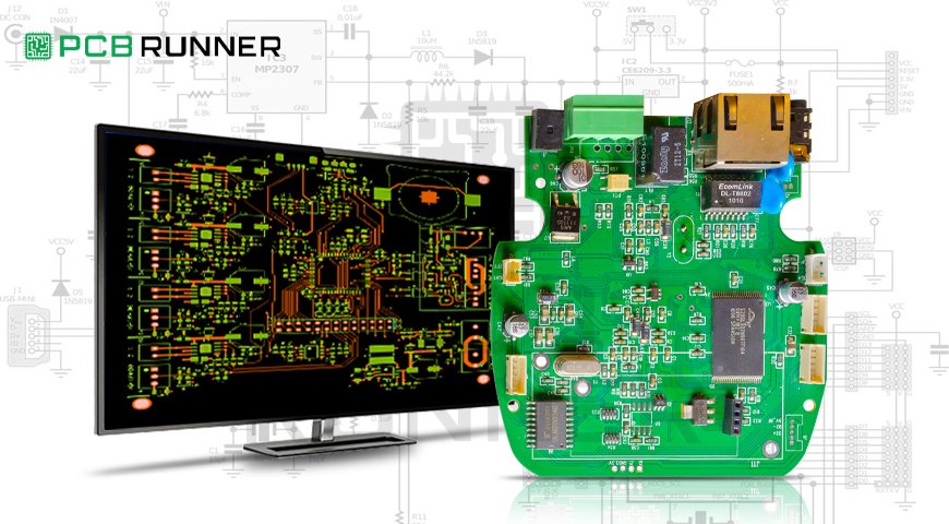
As the backbone of almost every electronic device, printed circuit boards (PCBs) hold everything from smartphones to medical devices. They help integrate the different components, ensuring electricity moves seamlessly. However, now and then, things might go awry. One frequent issue with electronic devices is a short circuit.

If you are involved in the design, maintenance, or production of electronics, knowing how to locate short circuits is essential. This blog aims to share practical techniques to identify short circuits on PCBs. We intend to simplify methods, putting them in easily relatable terms. Be it a novice or an inquisitive reader, we hope the content motivates you to engage with PCBs and resolve problems they present.

What is a Short Circuit on a Printed Circuit Board?

As the saying goes, “a short circuit is an event that occurs when there is an unintentional connection between two points in an electric circuit.” Let’s say we are dealing with a positive and negative end with a pipe allowing unrestricted flow. If we make an opening in the pipe, for some reason, the water would start flowing sideways. “Shorting” would allow the water to go sideways, and if it’s uncontrolled, things are bound to break.

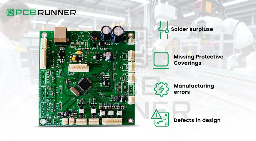
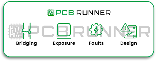
Shorts in printed circuit boards can be caused by:

  • Solder surpluses (small accumulations of solder connecting two traces)
  • Severed or missing protective coverings
  • Manufacturing errors
  • Defects in the design lead to the PCB design shorts process.

Finding these shorts and the associated repairs is significant due to the safety and performance cost.

pcb manufacture

Why Is It Important to Track Down Short Circuits in PCBs

Short circuits can result in serious issues:

  • Wrong Device Behavior
  • Possible Safety Concerns
  • Additional Expenses

Loss of Time in Production

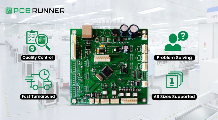
Detection of short circuits in PCBs is an utter priority in avoiding excessive spending and needless stress, which is why many suppliers and manufacturers of printed circuit boards in the UK employ thorough testing practices during the fabrication and assembly of the PCBs.

Detection Short-Circuit Tools

Before discussing the methods, it is pivotal to start with the tools that the professional utilizes:

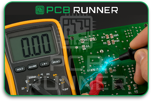
  • Multimeter: Basic tools to measure continuity and resistance
  • Thermal Camera: Identifies excessive heat on power apply boards
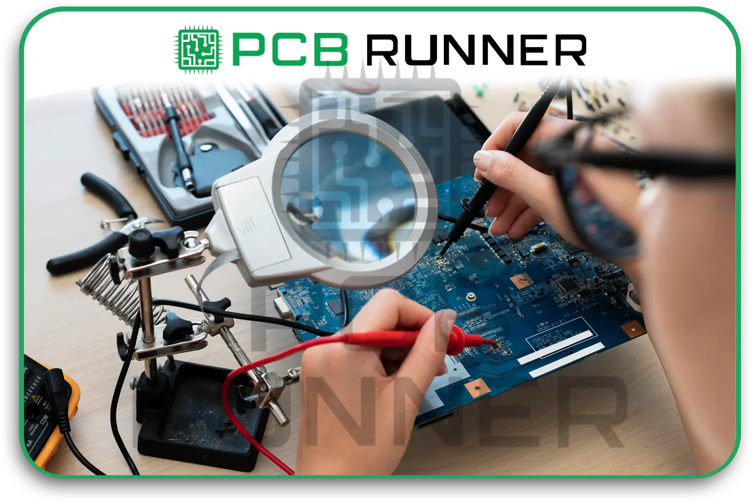
  • Microscope and Magnifying Glass: Checks the components to see solder connections
  • Automated Optical Inspections: Scanners that check for surface defects
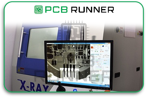
  • X-ray Inspection: Reveal concealed shorts in multilayered boards.
  • In-Circuit Testers (ICT): Probes that check the electrical continuity of circuits automatically.
  • Fly Probe Testers: Moveable probes for small-sized production and prototypes.

There are advantages and disadvantages to each approach. In this case, using more than one technique will enhance precision.

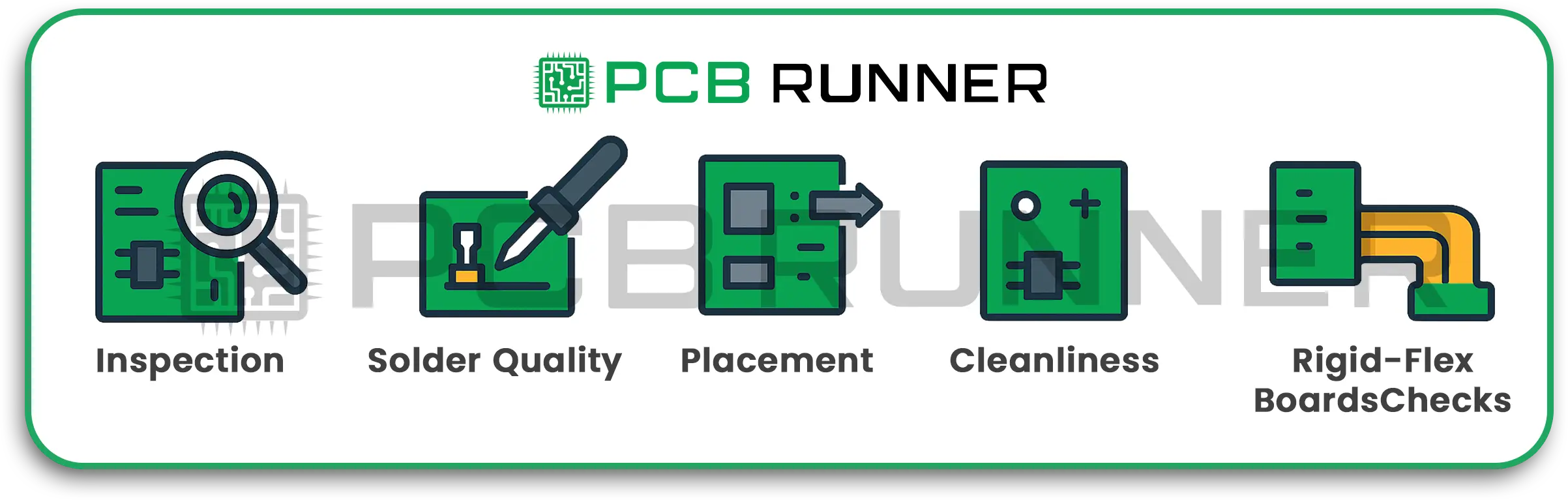
Identifying Short Circuits on PCBs: A Comprehensive Guide 

1. Visual Inspection 

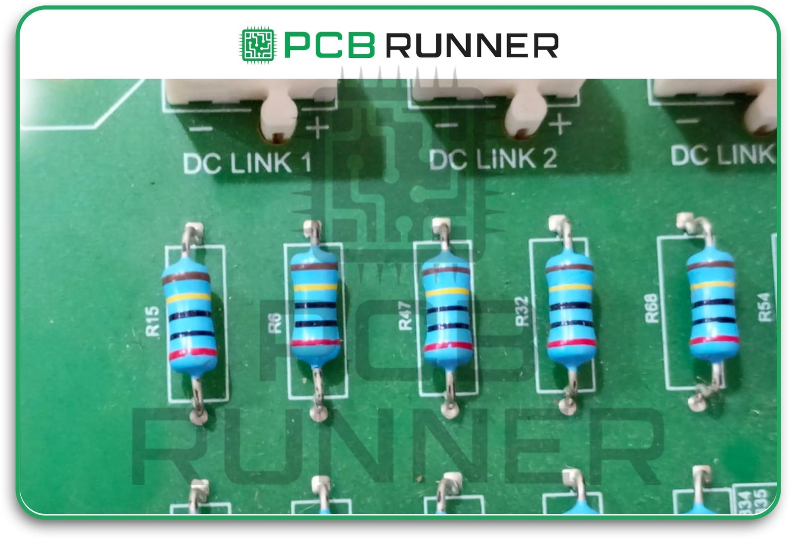
Let’s begin with the basics. Examine the PCB more closely under a light with a magnifying glass. Ensure there are: 

Solder bridges that join either a pin and a pad or two pads.

Insulation that is cracked or damaged on the traces.

Copper that is either rogue or scratched, connecting two paths.

Solder that is poor or missing gaps. 

This usually helps to identify and resolve many issues before the PCB is powered. A lot of shorts are a result of excess solder or debris. 
Visual Inspection

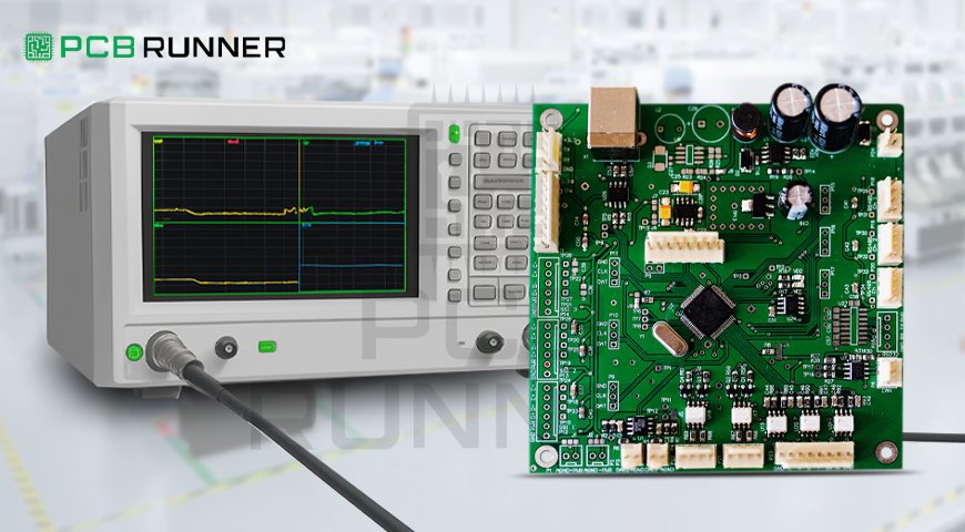
2. Using a Multimeter for the Continuity Test 

This is where a multimeter will come in handy. Set it to continuity mode (the meter beeps when two points connect). Then, do the following: 

Hold one probe on the power trace or the input pin.

Hold the other probe on the ground or a suspicious neighboring trace. 

If the multimeter beeps when it shouldn’t, that is an indication of a short. Another test is to check resistance. Very low values between points that are supposed to be isolated could indicate a short.

Multimeter for printed circuit boards

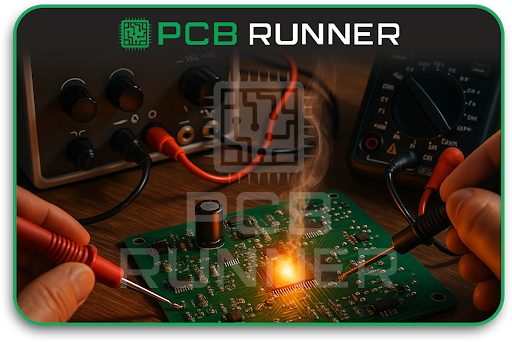
3. Power-On Testing (With Caution)

Powering the board might sometimes identify shorts due to overheating or odd operations. Be careful in this case:

Use a current–limited power supply to apply power and prevent damage.

Check if any area rapidly heats, hot areas are usually the result of shorts.

Check for indicators such as a burning odor or smoke (if noticed, stop immediately).

printed circuit board manufacturers uk

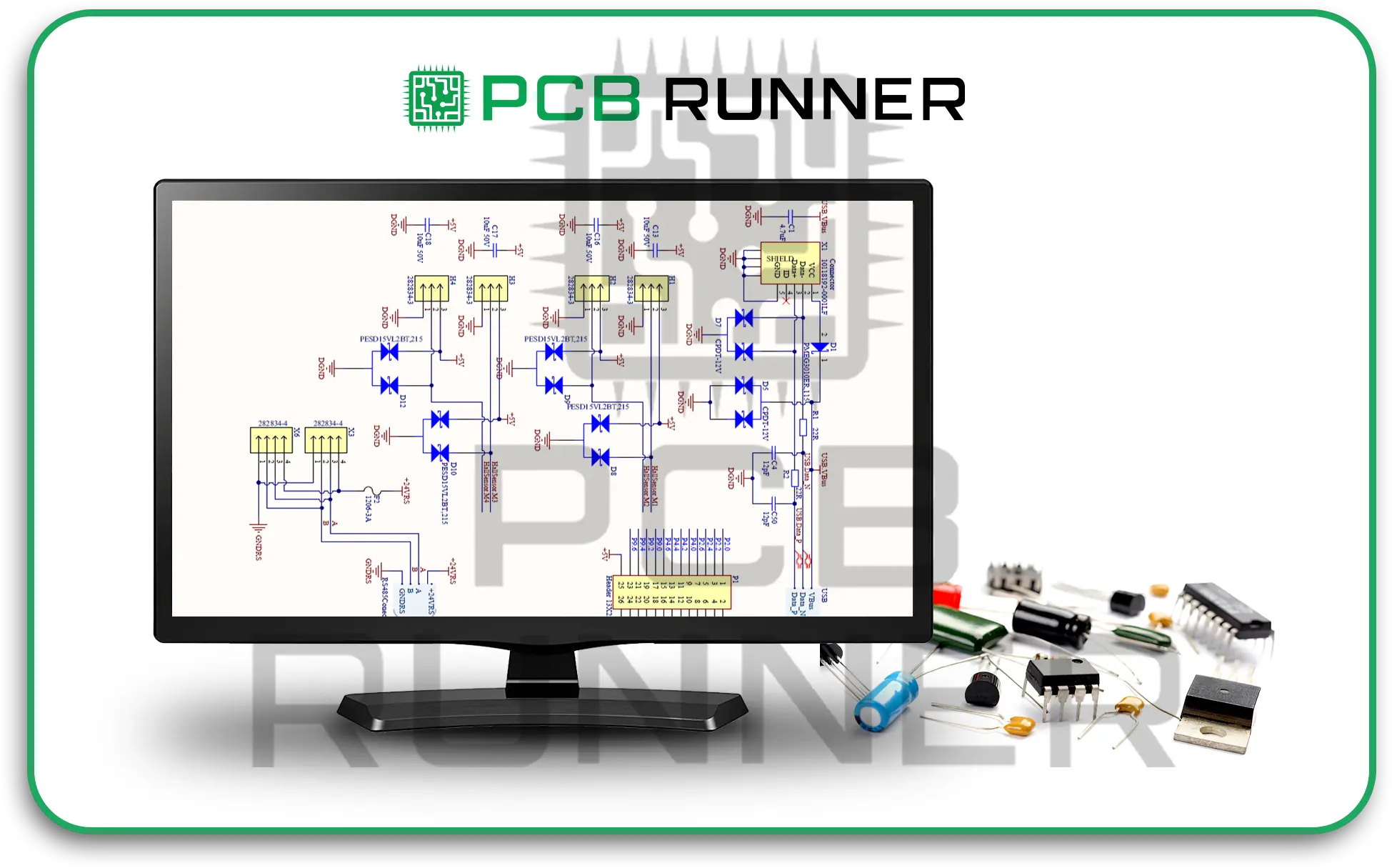
4. Advanced Testing: Automated Optical and X-Ray Inspection

For the production of high-volume or high-add-density PCBs, the following approaches are functional:

AOI: Uses Automated Optical Inspection to take high-quality pictures and detect solder bridges or misplaced metal using software algorithms.

X-Ray inspection: Useful for multilayer boards, as the shorts usually occur in layers that are not externally visible. X-ray is capable of seeing solder bridges under BGAs and other concealed defects.

These approaches provide remarkable accuracy, though they require additional apparatus.

high-add-density PCBs

5. In-Circuit Testing (ICT) and Flying Probes

ICT is deployed along with a “bed of nails” fixture to check physical contact of exemplary assembled boards with printed circuits and detect shorts by resistance and continuity tests. Flying probe testers can operate without fixtures, which makes them useful for prototypes as they tend to be tested without specific setups.

These techniques diagnose shorts at the component level and improve the PCB quality assurance.

Guidelines for Locating Shorts in Complicated PCBs 

Locating shorts in multilayer and smaller boards can be sophisticated. Below are some valuable tips: 

  • Use the schematic and the PCB design to narrow down potential areas to be checked. 
  • Always check the vicinity of the power supplies and ground planes since this is the common area for shorts to occur. 
  • While powered under thermal imaging, search the area using a thermal camera for hotspots. 
  • Take a portion of the area and check the limited places. 
  • Safely remove parts one at a time to exposed regions to isolated shorts to safely exposed regions.

Addressing PCB Design Short Issues 

Prevention is better than cure! Good practices regarding PCB shorts matters: 

  • Maintain proper gaps between traces. 
  • Steer clear of sharp angles as well as overlapping pads. 
  • Make use of automated clearance and spacing design rule checkers. 
  • Perform thorough checks on prototypes prior to full-scale production. 
  • When shorts arise as a result of excess soldering: 
  • Make use of a de-soldering braid or solder wick to remove excess solder. 
  • Rework joints to hot air or soldering iron-controlled precision methods 
  • Wash the PCB using isopropyl alcohol to remove flux and dirt residues. 

Conclusion: Detecting Shorts in PCBs Simplified 

Safeguarding electronics systems and devices from short circuits hinges on trusting the PCB in question. Trust is carefully earned through compelling visuals and physical checks.

Detecting short circuits is a crucial skill for PCB fabrication and assembly work. The multimeter and efficient inspection methods make the task straightforward. 

Short standard PCB detectors and thorough scrutiny from experts guarantee precision in project delivery, from initiation through to culmination. PCB Runner is a prime example of such companies.

With the knowledge and methods detailed above, you can increase the efficiency and quality of your PCB projects. Turn the issues you face into reliable solutions.

PCB Layout Design

PCB Layout Design Best Practices for Reliable Circuit Performance

A printed circuit board (PCB) is an essential part of most electronic devices and systems today. A well-designed PCB enables seamless and dependable operation of the device, whether it is a simple gadget or a sophisticated aerospace gadget. Circuit engineers face the challenge of creating dependable circuits. The secret of a successful PCB is often found in the PCB layout design, which involves determining the placement of components and connections on the board. In this post, I will provide an in-depth PCB layout design guide to ensure efficiency and PCB reliability for devices and systems.  

Components of PCB Layout Design System  

Let us start with the fundamentals. A PCB consists of a flat, insulating board, with electronic components (like a capacitor, microchip and resistor) interconnected via a copper “trace” or “line.” The copper components share electrical pathways. The design layout shows the schematic diagram of the components and also provides an outline of the connections. A practical design layout will ensure the circuit operates as expected, can be produced through existing or novel manufacturing processes, and PCB reliability is guaranteed throughout the lifecycle.

Components of PCB Layout Design System_

What Is The Importance of PCB Layout?  

Think about building a city; roads must be planned; otherwise, there will be traffic jams and accidents. The exact parallel applies to electronics, where there are traces that must be laid expertly so that signals do not weaken or interfere. These details and, more fundamentally, a good layout are a must to resolve underlying and potential issues.  

Best Practices for PCB Layout Design  

1. Start with a Clear Schematic.  

Before any parts are mounted on a board, you must first have a schematic diagram that shows every component and connection. The schematic portion is a guide for layout and helps you not miss any connections.  

2. Define the PCB Size Early  

Sketch and set the dimensions of the board and its shape first. Doing so allows you and the shape of the device or enclosure that you are working with.  

3. Build or Use Standardised Component Footprints  

Every component is represented on the PCB by a footprint that indicates the zone of the component to be soldered to the board. Use industry standards footprints to avoid any last-minute issues during assembly.  

4. Thoughtful Placement of Components.  

The component assignments are perhaps the most crucial portion of the circuit. Think of working on the layout as a puzzle; parts that help one another work must be grouped.

Keep Components Close to Minimise Voltage Drops

  • Make sure to leave space in between components for heat to dissipate and for testing access.  
  • Avoid placing components in a way that makes assembling the circuit challenging.  

Traces Should Be Short and Direct  

  • Short and straight traces are superior to long and winding traces as they minimise signal delay, noise, and loss. Long and winding traces are prone to interference and therefore affect the performance of the circuit.  

Proper Trace Widths Should Be Used  

Follow the manufacturer’s standard design rules on the width and spacing of copper traces to avoid overheating. 

Practices for PCB Layout Design

Work with your PCB Manufacturer to Determine Electric Needs  

Signal integrity, impedance, and the resistance to signal flow are all affected by the arrangement of layers of copper and insulations. Work with your PCB manufacturer to get a stack-up that suits your circuit’s electrical needs.  

1. Keep Analogue and Digital Sections Apart  

Avoid mixing the noisy digital signals with sensitive analogue lines, as it will cause interference. In order to maintain signal clarity, set these sections apart in your layout.  

2. Add Planes for Power and Ground  

Solid copper planes are superior to traces when representing power and ground as they minimise electrical noise. The use of power and ground solid planes enhances stability.

3. Position Decoupling Capacitors Adjacent to ICs

Decoupling capacitors eliminate noise from power lines. For maximum effectiveness, ensure decoupling capacitors are placed as close as possible to the power pins of the chips.  

Consider Manufacturing Constraints  

The PCB has to be manufactured. These considerations regarding the design will help ease the fabrication of the board:  

  • Comply with the minimum spacing requirements.  
  • Do not place components where soldering is challenging.  
  • Select parts with industry-standard footprints to guarantee ease of procurement.  

Your circuit board silkscreen should include designators, logos, and telltale markings like the reference designators, which tell the assembler where “pin one” is. These markings assist not only in assembly but troubleshooting as well which is invaluable in the repair process.  

Adhering to Guidelines  

Signal issues, overheating, and challenging manufacturability are common issues that arise when not following the provided guidelines. These are in place to ensure reliability. Your circuit will experience enhanced robustness and reliability to environmental factors, and ease of manufacturability for diverse production scales, most advantageous when a complete turnkey assembly is planned, where the board undergoes full build and thorough testing.  

Considerations Based on Circuit Types  

  • High-Speed Digital Circuits: Maintain well-defined, controlled impedance paths.  
  • Analogue Circuits: Maintain a proper, digitally quiet zone with grounded physical distance to avoid interference.  
  • Power Circuits: Incorporate thermal reliefs on wide traces to mitigate the risk of overheating.  
  • Mixed Signal: Logically section the board and separate analogue and digital areas with controlled interconnections.

Your application’s requirements will profoundly influence the layout considerations.

Thoughts on Seeking Assistance.

The process of designing a custom printed circuit board (PCB) may become intricate. The careful review of your designs by experienced manufacturers and assemblers helps in correcting mistakes early on. They guarantee that your PCB fabrication assembly will adhere to your design intent and quality benchmarks.”

For instance, some firms will review your electronic board design files for free and provide prompt responses to queries around the clock. Working with a dependable PCB provider will assist in efficiently converting your circuit board layout into a tangible product.

Conclusion

Effective PCB layout design incorporates creativity and technical knowledge. It demands a systematic approach and a good grasp of the intricacies of electronic systems. Following these best practices, your custom printed circuit boards will be dependable for the entire life of your project: starting with unambiguous schematics, strategic component placement, meticulous routing, and trace routing alongside manufacturing considerations.

Those looking to deepen their understanding, resources like Cadence’s “PCB Design Layout Guidelines” explore achieving high-quality designs in significant detail.

As you approach the production and assembly phases, collaborate with seasoned manufacturers to guarantee that your PCB circuit layout will be transformed into hardware that operates as designed. For technical assistance and project support in professional-tier PCB manufacturing and assembly, specialised companies such as PCB Runner are a good fit.  

For more in-depth PCB layout concepts, you may refer to Cadence’s blog on PCB design layout guidelines (Resource).

IPC Inspection

IPC Inspection: Important Rules and Best Practices

Think about trying to bake a cake without checking if it’s done in the middle, or building a bridge without measuring if the supports will hold. In electronics, inspection is like the last step check: it makes certain that every product functions correctly and safely. This is where IPC inspection comes into play.

For anyone involved in the PCB’s design, assembly, or manufacture, knowing the IPC inspection guidelines is essential. It enables makers, engineers, and businesses to identify defects in the design, gaps in the manufacturing processes, and to avoid failures, ensuring the devices delivered are compliant with the industry standards and user expectations.

So, let me introduce you to IPC inspection, best practices, and understand why it is essential from custom PCB assembly to sophisticated rigid-flex boards.

What is IPC Inspection?

IPC is a worldwide association that issues standards for the design, fabrication, and inspection of printed circuit boards (PCBs) and electronics assemblies. IPC is the “Institute for Printed Circuits,” but now it is best known by its short form.

IPC inspection is the process of evaluating PCBs and assemblies in accordance with the IPC guidelines. These evaluations are conducted at multiple stages:

  • Post manufacturing: Bare board inspection
  • Post assembly: Checking finished products
  • During the process of rework or repair

What’s The Objective? Spot problems in the board and make sure it is up to standard at every level of quality control.

What is IPC Inspection_

Why Are IPC Inspection Rules So Important?

Think of IPC rules as the “recipe book” for electronics. These guidelines make sure that each custom PCB assembly and every rigid-flex board is:

  • Safe for use
  • Durable
  • Functional as intended

By skipping inspection or ignoring these rules, you’d risk creating short circuits, recalls, or dangerous failures. Nobody wants their fancy new gadget to die an early or an unexpected, sudden death.

Key IPC Inspection Rules: In a Nutshell

IPC has numerous standards, but two of the most noteworthy ones are:  

  • IPC-A-600: This standard is for bare boards and highlights how a perfect PCB should be and what flaws are not acceptable.  
  • IPC-A-610: This standard is for assembled PCBs, which includes soldering, component placement, and the overall cleanliness of the board. 

Key IPC Inspection Rules_ In a Nutshell

1. Visual Inspection  

Every board goes through a detailed inspection:  

  • Do the traces (the small copper pathways) look clean and intact?  
  • Are the holes clean?
  • Are the layers properly aligned?  
  • Is there any physical damage, like scratches or burn marks?  
  • For rigid-flex board designs, are the flexible zones free of splits or tears and smooth?  

2. Solder Joint Quality  

For solder joints,  

  • The exposed surfaces should be shiny, smooth and not cracked.
  • Prevent excessive solder, “solder bridges” which can inadvertently connect pads and cause a short.  
  • Critical IPC requirements are: the exposed pad and component lead must be a precise cut percentage of the solder joint.  

3. Component Placement

For the components,  

  • Orientation should face the right direction.  
  • Components should not only be centred on their respective pads but also at the right height.
  • Should not be tilted or “tombstoned”.  

4. Cleanliness and Residue Checks  

Ensure there is no leftover soldering flux, dust or hand smudges. Any of these can cause system failure in the long run.

5. Extra Checks for Rigid-Flex Boards  

Rigid-flex boards have some unique considerations:  

  • See to it that the flex section is able to bend without any cracks appearing.  
  • Look for any signs of delamination.  
  • Pulling apart layers due to delamination.  
  • Confirm that stiffeners and connectors are securely attached.  

As an example, we can use the IPC inspection rules for a rigid-flex board. 

Best Practices for Effective PCB Inspection

You can have the best technology and most advanced designs, but if you skip careful checks, success is uncertain. Here’s how top pcb manufacture teams approach inspection:

1. Follow a Step-by-Step Process

  • Inspect at every stage, from raw materials to final assembly.
  • Catching errors early saves time and money.

2. Use Automated and Manual Inspections

  • Automated Optical Inspection (AOI): Cameras and software scan boards to spot even tiny faults.
  • Manual Inspection: Human inspection handles complex boards or places machines can’t see.
  • For tough designs, such as high-density or custom PCB assembly, both are essential.

3. Test for Function, Not Just Looks

  • Power-up tests check if every circuit works as planned.
  • Boundary scan and X-ray inspection spot problems hidden inside layers or beneath chips.

4. Train Staff on IPC Standards

Quality starts with knowledge! Teams should know the latest IPC-A-600 and IPC-A-610 rules. Mistakes often happen when people miss small but important details.

5. Document Everything

  • Keep detailed records of inspections.
  • This helps trace problems and improves the process for future builds.

Common Problems Found by IPC Inspection

  • Solder bridges: Unwanted connections that can short the circuit
  • Open circuits: Broken connections (like a street with a cut-off bridge)
  • Wrong or missing parts: Components facing the wrong way, or not installed at all
  • Poor bonding between rigid and flex parts
  • Contamination: Dust or oil causing problems over time

With strict inspection, these issues are spotted before boards reach customers.

How PCB Inspection Benefits You

Whether you’re an engineer, maker, or tech company:

  • Safety: Avoids dangerous device failures
  • Reliability: Products last longer, build customer trust
  • Faster Launches: Fewer delays fixing hidden flaws
  • Cost Savings: Prevents expensive recalls or repairs

Tip: When choosing a pcb manufacture partner, always ask about their IPC inspection process. Reliable partners never skip this step!

Best Practices for Custom PCB Assembly and Inspection

  1. Define Inspection Criteria Early: Decide which IPC class your board needs, Class 2 (industrial), Class 3 (mission critical), etc.
  2. Work Closely with Your Assembler: Share your board design and requirements. Good custom PCB assembly teams will suggest inspection steps.
  3. Embrace Both Manual and Automated Inspections: For precision and thoroughness.
  4. Never Skip the Final Functional Test: It’s your insurance against hidden errors.
  5. Update Inspection Processes as Tech Evolves: New designs, like complex rigid-flex boards, need updated inspection strategies.

For the Curious: Going Deeper Into IPC

Want to become an inspection pro or simply understand more? Learn about IPC’s role and standards in electronics manufacturing with resources straight from the source.

Conclusion: Inspection Is the Unsung Hero (And PCB Runner Gets It Right)

From the outside, electronics look smooth and simple. But inside, every device’s reliability depends on careful inspection at each step. IPC inspection isn’t just a checklist, it’s a mindset, a habit of excellence. For anyone working with pcb inspection, rigid-flex board builds, or custom assemblies, knowing, and following, IPC rules is non-negotiable. That’s how modern technology stays smart, safe, and long-lasting.

Companies like PCB Runner put IPC inspection at the heart of their process, so you can count on circuits that meet the highest standards, every single time.

In electronics, a careful eye saves the day. Never underestimate the power of a thorough inspection!

Double-Sided Prototype

Double-Sided Prototype PCBs: Manufacturing Process

Have you ever wished you could bring your electronic concept to life? The first step of that journey is usually a board, a PCB. But what if your concept requires a mix of portability, energy efficiency, and flexibility? In that case, double-sided prototype PCBs are just what you need. They provide a robust base for engineers and inventors for their next greatest piece of work.

Understanding Double-Sided Prototype PCB

A double-sided prototype PCB is a type of prototype PCB that has copper pads and traces on the top and bottom sides. With this prototype, engineers and designers can connect components on two layers instead of one.  

Now, why is that significant? Let’s visualise that you are building a model city. If you can only place roads on the ground (single-sided), you might quickly run out of space and options. If you can add an overpass (double-sided), you can now have more cars and creativity flow. That is the exact benefit that we have here.

What Is a Double-Sided Prototype PCB

How Double-Sided PCBs Are Made  

Curious to find out the steps involved in double-sided prototype PCB creation? This is how it looks in a nutshell:  

Every board begins with a digital sketch. The first step is laying out all connections which need to be done in advance for a practical layout.

  • Choosing Materials: The insulating base (generally FR-4) is sandwiched between copper sheets.
  • Drilling: The upper and lower layers can be connected through small holes, which can be likened to little elevators or tunnels.  
  • Plating Through Holes: During prototype and PCB fabrication, metal is added inside the holes. This provides both sides with an electrical connection, which enables the transfer of signals and power.  
  • Etching and Printing: Circuit paths are being etched, and both sides of the board can be printed with their respective patterns.  
  • Adding Solder Mask and Silkscreen: Protective layers are added to the board while simultaneously labelling the critical components.  
  • Final Testing and Cutting: The boards are checked for accuracy, then cut to shape to the desired dimensions before being dispatched.  

Why Use Double-Sided Prototype PCBs?  

Imagine for a moment that you are testing electrical circuits for a new device. You’re looking for a space that can accommodate a few chips but not a bulky and multi-layered board. This is where double-sided PCBs shine.  

Top Benefits  

  • Space-Saving: The old saying, “Two Heads are Better Than One,” perfectly captures the use of both sides as components and tracks can be placed on both sides, which is a boon for compact designs.  
  • Increased Versatility: Excellent for PCB prototype runs and small production batches.  
  • Stronger Circuitry: More routing flexibility reduces the number of crossed wires, increasing the reliability and sturdiness of the build.  
  • Cost–Efficient: Fewer cross-sections than multi-layer boards. Less complex than multi-layered boards and more robust than single-sided PCBs.

Why Use Double-Sided Prototype PCBs

The Manufacturing Process

Printed circuit board manufacturers work on processes like checking for design match and correctness. Most well-known PCB manufacturers pay special attention to every step while working on double-sided PCBs.

  • Verification of the Digital Project: Checking the design against digital files.
  • Cutting and Drilling Material: The exact steps, like cutting and shaping materials into boards, and drilling to define thousands of precisely measured holes, are done with the help of CNC machines.
  • Through-Hole Copper Plating: The layers are connected with top and bottom “treeshouses” via ladders.
  • Soldermask and Circuit Etch: Circuit markings are put on boards to help the device detect malfunctioning components. This is to help decrease the possibility of the device failing.
  • Label and Silkscreen: The described steps help to place the PCB in sequential order. The board is “marked” with attention.

Final inspection is done by marking every board for the missing signal paths before assembly. As described, every board is treated the same and pending check for open and shorts.

Marking for every piece is done simultaneously to help with labelling.

Recommendation: Spend less times looking for business needed for prototype designs and order from those who convey up to date step by step processes.

Assembling the Prototype: From Bare Board to Functional Circuit

Board construction begins after a thorough check of the fabrication steps. Turn to PCB Assembly UK Services for the following:

Component Placement: Every chip, resistor, and connector is mounted on the board. This can be Down either by a tiny machine or rather careful hands.

  • Soldering: Creating a durable long long-lasting bond. For double-sided boards, the soldering is done on both sides.
  • Quality Checking: Every single circuit is visually checked, sometimes using X-ray equipment, to guarantee flawless and perfect connections.

Why Prototypes Matter: Testing Electrical Circuits

No one is perfect, and neither is a device, hence the importance of testing. Prototypes are essential as they help to fine-tune and perfect a design. They are helpful in performing the following:

  • Thermal stress, ensuring nothing is overheating or cracking.
  • Screaming and checking for open or short-circuits.
  • Signal tests.
  • Thermal testing.

Prototypes are essential in testing and can save a lot of money when scaling.

Maximising Strategies for Double-Sided Prototyping

Strategically Place Components: Avoid placing sensitive sections near heat and interference.

  • Use Labels: Clean labels ensure easier and faster testing and fixing.
  • Check for Manufacturer Capabilities: Not all PCB manufacturers have the same features; check for minimum hole size or special materials.
  • Don’t wait until it’s done to check; the design should be done as early in the prototype lifecycle to improve wiring or logic changes.

Key Takeaways for Inventors and Makers

  • Double-sided prototype PCBs offer a sweet spot of complexity, cost, and flexibility.
  • They’re perfect for prototyping, small production runs, and learning new tricks about circuit design.
  • Services like pcb assembly uk bring extra value, letting you go from idea to tested device, fast and reliably.

Want a deep dive into double-sided PCB manufacturing? Check this authoritative guide on manufacturing processes.

Conclusion: A Trusted Provider for Double-Sided Prototyping 

Double-sided prototype PCBs help realise big ideas in a compact form. They enable engineers, students, and makers to test, refine, and launch innovative electronics in record time. PCB Runner, as one of the leading suppliers, supports advanced fabrication, flexible prototyping, and expert assembly services for the UK and Europe.  

When you’re prepared to create, test, and learn, don’t go on a one-sided adventure. Double up and double your opportunities.

ENIG Surface Finish

Top Advantages of Using ENIG Surface Finish

You choose the finest components. You adhere to the guidelines. But if you skip the final coat of paint, the car will rust and fade. That’s akin to what a PCB (printed circuit board) can undergo if you omit the final protective layer, which is a surface finish.

In electronics, surface finishing adds value by protecting, joining, and increasing functionality; it integrates more advanced features. From many alternatives, ENIG surface finish is recommended for new designs as well as on dependable circuits. ENIG stands for Electroless Nickel Immersion Gold. 

Let’s see what features encourage engineers and makers, as well as the finest HD IC PCB suppliers, to choose ENIG.

What is ENIG Surface Finish

A PCB surface finish ENIG is two thin layers of a bottom layer of nickel as a base, and a thinner overlay of gold as a thin layer on the PCB gold finish. All layers of copper pads in every PCB are plated with nickel to protect the copper. Gold will keep the Nickel and enhance the surface finish. This helps to maintain the longevity, function, and preservation of the board throughout usage, exposure, and environmental conditions.

What is ENIG Surface Finish

ENIG Surface Finish: The Working Steps:

Step 1: Copper Cleaning

Wash the copper surface of the board to remove dust and oily materials.

Step 2: Nickel Layer Forming

The board is immersed in a nickel layer-forming solution, where a layer of nickel is deposited, protecting the copper.

Step 3: Gold Layer Application

Roll the board to gold bath 2, where gold is deposited as a thin layer on the surface.

Step 4: Surface Inspection

Every step is verified. The result is a surface enduring a flat and durable finish of high quality, which is ready for assembling the board.

ENIG Surface Finish_ The Working Steps_

Why ENIG? The Key Advantages

1. Amazing for Fine Pitch and High Density (HDI PCBs)

If you are passionate about compact and innovative technology like smartphones, tablets, and wearables, you are familiar with the need for densely packed components on PCBs. ENIG surface finish is perfect for these dense, tiny components and ensures HDI PCBs are equally complex and compact.

2. Soldering Accuracy Improvement

Think of glue that works so effectively, it can be unreliable at times. ENIG entirely smooth surfaces that give u even finishes allow for soldering ( the installation of chips and wires on boards) to be done with precision. Every hinge and turn can now be done with precision.

3.Durability and Resistance

Devices that decide to malfunction and ‘quit’ early are something we can all agree on. ENIG surface finish protects boards much like a military grade armour plating. It works effectively at preventing rust and all forms of corrosion. When combined with harsh conditions, such as humid or coastal climates, the outer layer of gold nickel is like the shields of your devices, helping them function for a long longer.

4. ENIG is RoHS Compliant

More and more restrictions are being put in place for the harmful components that can be added to finishes. ENIG gold surface finishes are now marked as being non-toxic and safe for the environment.

5. Extended Storage Availability

Have your plans fallen behind schedule? ENIG is able to keep your boards “fresh” longer. Boards using ENIG finish can often be kept for months or even years without any significant performance degradation or extensive cleaning prior to assembly.

6. Surface Finish Quality

Performance also improves with ENIG, as its aesthetics are a significant consideration. This finish gives each PCB a mirror-like surface, which makes it possible to print fantastic traces onto the PCBs. Smooth assembly is also without any rough patches or bumps to ruin those tiny traces.

Why ENIG_ The Key Advantages

Real-World Example: ENIG and Modern Electronics

Have you ever had a look inside a smartwatch or a fitness tracker? They often contain a very compact gold-plated PCB, which is a hallmark of ENIG and its ability to keep these devices reliable and small, protecting them from sweaty wrists and bathroom splashes.

ENIG is the choice for automotive, aerospace, medical devices, and even smart home devices when the stakes are high and the space is at a premium.

ENIG Surface Finish vs. Other Surface Finishes

Feature ENIG Surface Finish HASL Surface Finish OSP/Other Types
Surface Flatness Excellent Not great for small parts Varies
Solderability High Moderate Moderate
Durability High Can crack/wear Lower
Lead-Free Yes Often no (if leaded) Yes or No
Lifespan Long Shorter Short/Medium
HDI/Prototype Use Ideal Not preferred Sometimes

Where ENIG Excels: Product Highlights

  • HDI PCB Applications: Ultra-small sizes, high complexity.
  • PCB Prototype Runs: Perfect for testing new ideas where reliability matters.
  • General PCB Printing: When you want predictable results and easy assembly.
  • Sensitive Devices: Medical, aerospace, and defence use ENIG for maximum safety.

Suggestions to Consider for Various Project Types

ENIG is ideal for those working with HDI or congested areas. No tombstoning or chip-out “falling-out” is possible.

Best long-term durability performance? ENIG-prepped boards will not degrade over time.

Have to pass strict compliance? ENIG is lead-free and a widely accepted global standards which aid in passing compliance for numerous countries.

Trying out new concepts? ENIG’s ability for fast-turn prototyping takes the hassle out of turning ideas into reality.

The Human side: Build your ideas more effectively.

Imagine baking cookies: rushing the bake and not using non-stick leads to cookies baked and burnt, stuck to the pan. PCB finishing is the same. No cooking electronics “finishes” means electrons will “glue” to unwanted areas, causing critical device failures.

Struggling with chargers for devices? Everyone wants functioning devices and does not want to deal with devices turning into non-functioning bricks. ENIG’s finishing takes the worry out with reliability behind using getting connected without mystery breakdowns.

Addressing the Most Frequently Asked Questions:

Q. Is the cost of ENIG high?
A.It sure can be more expensive when compared to simpler finishes like HASL. However, it pays off in the long run by lowering defects, increasing yield, and enabling new designs.

Q. Is ENIG suitable for my prototype?
A. Yes. Many prototype shops, ENIG, which makes testing quick and dependable.

What about health and environmental standards? ENIG processes are lead-free, making them more supportive of eco-friendly policies.

Expert Insight: The Future of Surface Finishing

With the continuing miniaturisation and intelligence of electronic devices, finishes like ENIG will become increasingly common. The high demand for surface finish quality and ENIG’s consistent reliability and adaptability make it a perfect fit for advancing technology. To understand more about ENIG and its many benefits, read this guide.

Final Thoughts: ENIG and PCB Runner

In short, ENIG provides distinct value for builders, testers, or purchasers of complex PCBs. For professionals and hobbyists alike, ENIG’s smooth and robust finish makes it easy to anticipate future needs.

If you’re focused on maintaining rigorously high standards for boards, particularly for contemporary HDI designs and rapid prototypes, ENIG merits your consideration. For outstanding work, one can rely on PCB Runner, which offers unparalleled trust and top-grade surface finishing PCB fabrication for every project without compromise.

In the background, delivering the best for your electronics, enhancing safety, and preparing them for the future, ENIG and PCB Runner work hand in hand where innovation meets trust.


PCB Manufacturing Company

Why PCB Runner Is a Reliable PCB Manufacturing Company?

Look around you, and you will see a number of devices that rely on technology. The smartphone you use in the morning. The laptop you use for studies. The TV that shows you your favourite shows. The most crucial piece of technology that all of these devices use is a printed circuit board, or a PCB. A PCB needs to be robust and reliable for a gadget to work optimally. Furthermore, selecting the right printed circuit board manufacturers is critical, especially if you are searching for a circuit board supplier UK or a quality PCB production UK.  

What is a PCB and Why Is It Important?  

A printed circuit board PCB is essential in today’s world. It is like the nervous system for gadgets and makes sure that all the functions work well together. Top gadgets and devices won’t be possible without the right printed circuit board. This is precisely why engineers, electronic hobbyists and companies need a reliable printed circuit board manufacturer that can do PCB assembly and production for them.

What is a PCB and Why Is It Important

Why the Right PCB Manufacturing Company Makes All the Difference  

Consider building a robot or a medical device. Now think about how frustrating it would be to realise the device is non-functional due to a poorly made circuit board. All that effort, money, and time wasted! The wrong supplier often leads to mistakes like these. This is the very reason why a lot of companies trust PCB Runner. They count on them for their circuit boards, whether it be for one prototype or hundreds for a new product launch.  

What Sets A Supplier Out Differently From The Rest  

Choosing a supplier often revolves around pricing. But here is additional information that you should never ignore.  

  • Quality Control: They need to be diligent. Double and triple-checking every board should be standard.
  • Fast Turnaround: Quick delivery means that your work schedule won’t be thrown out of order.
  • All Sizes Supported: The supplier should be flexible and assist you, whether you need one board or one hundred.
  • Problem Solving: What good is the supplier if the only information provided is through an automated service? Real people need to be answering your inquiries and resolving them.  

Some suppliers pass your work to someone else. For this reason, they disregard communication, support, and even the review portion of the work. At PCB Runner, everything is done in-house, including design, review, and manufacturing. This brings you total peace of mind throughout the process. 

What Sets A Supplier Out Differently From The Rest

What Are The Main Steps Of The PCB Manufacturing Process  

Let’s discuss what to expect by breaking it down step by step.

1. Finalising the Design

It begins with you. You or your engineer will devise a design and generate Gerber files, which will serve as the detailed blueprints for the PCB.

2. Selecting the Materials

Some PCBs need to be robust. Some must be flexible. PCB Runner offers a full range, from the traditional rigid boards to the latest flex and hybrid ones.

3. Board Printing and Etching

Your artwork is printed on copper plates, from which excess copper is etched away, leaving the desired circuit.

4. Drilling and Vias

Small holes for the “vias” connections are drilled. This is where the components will be soldered on later.

5. Solder Mask and Finishing

The board is covered with a protective finish (usually green), and the board is applied an exceptional finish is applied to protect from oxidation.

6. Rigorous Testing

Here is where the most focus is put on quality. Each board is tested electrically to ensure functionality prior to assembly.

7. Assembly (If Required)

If you place an order for complete PCB assembly, skilled workers and machines will place all chips, connectors and components on the board. Each procedure is performed error-free.

8. Order Fulfilment and Transport

Your PCBs or assemblies are sent to you, ready to be built or sold. They are carefully packed to ensure no damage occurs during shipping.

Why PCB Runner’s Method is Good for You

It doesn’t come from nowhere that PCB Runner is not simply classified as one of the PCB production UK shops. Why is that?

  • Human assistance is available at any time of the day, every day of the week.
  • Charges can be viewed instantly, and the files can be uploaded in minutes.
  • Your design is checked thoroughly by the team as part of a complimentary design review.
  • Solutions are implemented immediately instead of being stalled by drawn-out email exchanges.

You have complete transparency in the order processes.

Features Offered by PCB Runner’s Technology and Services

  • Complex HDI as well as flex and rigid flex boards, as well as simple single-layer PCBs, can all be found in one place.
  • Certification granted for military, medical, and aerospace work includes ISO9001 and IPC Class 2, 3, 3A.
  • Fulfilment is excellent for large orders as well as tiny batches.
  • After-sales assistance: Calls are answered by our technical team even after delivery.
  • Want to explore modern PCB trends in the UK? Check this expert article on modern PCB trends.

Maximising PCB and Assembly Services: A How-To Guide

  • Ensure the files are the best and most detailed possible. Errors at this stage are costly in time.
  • If you are doing something new, talk to your supplier. Companies like PCB Runner thrive on complex projects, so don’t be afraid to reach out.
  • Save time by selecting a supplier that offers a design review. It can prevent costly errors well before they are made.
  • Find out about after-sales services. Dependable firms offer strategic advice even after boards are delivered.

Conclusion

Selecting your PCB manufacturing company is an important decision. The best partners do not simply manufacture your boards. They enable you to design, assist in problem resolution, and facilitate your growth. Runner PCB differentiates itself from the competition with excellent industry knowledge, positive reviews, and superb customer service. With every order, you are guaranteed thorough inspections, prompt responses, and a dedicated team for your project.

For dependable circuit board suppliers UK, leading PCB production UK, and complete PCB manufacturing and assembly services, trust PCB Runner. They are known for circuit board fabrication and PCB assembly services in the UK. Begin your next project with a partner who prioritises your requirements and can help with innovations.

FAQs

Q: What advantages are there in using a UK PCB supplier?
A: For most people, local suppliers mean faster turnaround, straightforward shipping, easy shipping and better communication, especially in your time zone.

Q: How can I ensure that my boards are of high quality?
A: Choose companies that showcase their certifications, such as ISO9001, as well as those that test each board before shipping.

Q: Is it possible to order both single units and large quantities at the same time?
A: Absolutely! Proficient suppliers manage both prototype and volume production. For example, PCB Runner is prepared for both.

Q: What if my design contains an issue?
A: Companies such as PCB Runner will provide free engineering consultations and suggested revisions. They give recommended changes before the production phase.

Q: Is it easy to change suppliers?
A: Not really, but if you are attempting to change partners, send complete documents and request a test order.

EMC Testing

Top Reasons EMC Testing Matters for Electronic Devices

When using your favourite gadget or electronic device, seamless functioning is usually expected. What makes these devices dependable? One primary factor is EMC testing. It is not well known, but very crucial in electronics, especially for circuit board suppliers UK and companies focused on PCB production UK.

We will cover why EMC testing is essential, the connection with PCB manufacturing, and the fundamentals of EMC testing in accessible language so all readers can engage.

What is EMC Testing?

Electromagnetic Compatibility is what EMC stands for. This is a device’s capacity not to damage or be damaged by other devices. Let’s take a phone buzzing during a text near a speaker as an example of bad EMC.

 What is EMC Testing

Why do We Need EMC Testing?

Electronics have penetrated all aspects of human life. TVs, cars, even medical devices and traffic lights. Lack of inter-device compatibility can result in problems ranging from minor irritations to life-threatening risks.

Here are the main reasons you need to conduct EMC testing:  

  • Safety: Everyone, particularly in hospitals or on planes, is kept safe.  
  • Performance: Ensures that devices are fully operational all the time.  
  • Legal Rules: Numerous nations have EMC regulations which devices must be tested prior to sale.  
  • Reliability: Minimises issues and returns with the electronics.  

Why do We Need EMC Testing

How Is PCB Assembly and Manufacturing Connected to EMC Testing?  

Have you ever heard the saying “the heart of electronics”? That is the definition of printed circuit boards (PCBs). Each device we use, be it a phone, computer or microwave, has PCBs embedded in it.  

The PCB manufacturing company must collaborate with experienced circuit board suppliers UK and perfect the PCB manufacturing process to ensure that their boards pass the EMC tests and are reliable.  

What Are The Steps In The PCB Manufacturing Process?  

Let us oversimplify it, starting with the first few steps:  

  • Design: This is when the engineers fix all the components into the board.  
  • Printing: The circuits are marked with special printers.  
  • Etching: During this stage, chemicals will “carve” the board and create pathways for electricity.  
  • Drilling: Tiny bits create holes for components.  
  • Assembly: Assembly of components, such as connectors and chips, are done by workers/robots.  
  • Testing: The boards are tested by powering them to check for issues and including EMC.

EMC Issues During PCB Manufacturing in the UK  

While producing PCBs in the UK, special attention is given to passing EMC tests. Here are some real-world problems that can arise:  

  • Overcrowded devices in one area.  
  • Poor design on the PCB assembly. Close wires? Big problems!  
  • Cheap materials that do not adequately block signals.  
  • Bypasses in the printed circuit board assembly steps.  

Often, PCB fabricators in the UK comply with numerous measures to lower vertical interference with extra shields and clever layout designs.  

Why does every electronic device require EMC testing?  

Even simple electronics can pose issues. For instance, a toy automobile that activates a child’s radio is problematic. Or, a medical instrument that is “confused” by functions in a hospital is dangerous.  

Key reasons every electronic device must undergo EMC testing:  

  • Protects from accidents.  
  • Preempts product recalls.  
  • Complies with laws and regulations.  
  • Provides long-term savings.  

EMC Testing: How the Industry-Leading Suppliers Approach It  

Circuit board suppliers UK and top PCB manufacturing and assembly teams do these to pass EMC tests.  

  • Provide quality standards during printed circuit board assembly.  
  • Perform board-level quality checks before shipment.  
  • Design with EMC considerations from the planning stage.
  • Assist customers in resolving problems as soon as possible.  

If you want to make your PCB manufacturing and assembly more reliable, these tips might help.  

Testing is great, but we can improve more innovative design. Here is what experts suggest.  

  • Cut high-speed wires to reduce excess noise.  
  • Use ground planes, which are areas of copper that can soak up signals and help reduce unwanted noise.  
  • Spread out, instead of cramming hotspots together.  
  • Use good blocking materials to eliminate interference.  
  • Simulate EMC before creating the physical object.  

If these steps are taken, UK PCB manufacturing companies will be able to eliminate the majority of EMC problems before the production stage.  

Compliance and Global Standards: Their Importance  

There are stringent regulations regarding electronics sold across the globe. Therefore, reliable PCB manufacturing companies must ensure that the boards are tested to match the European Electronic Communications Committee’s standards (hyperlinked as an example). This helps ensure UK electronics function anywhere in the world.

EMC Testing Techniques

Here’s a sneak peek at how specialists evaluate circuit boards:

  • Radiated emission tests: Look at the signal output of the device to see if it is leaking any data that it should not be.
  • Immunity tests: Make sure that the device is not interrupted by outside signals like a phone ringing.
  • Conducted emission tests: Look for any data signals that are leaking through cables.
  • Environmental tests: Simulate shaking or rapid temperature changes.
  • Every step ensures that the PCB manufacturing process is being done correctly.

What To Do if Devices Have Failed EMC Tests

While it’s not the worst-case scenario, it does mean that more work needs to be done. If a device fails a test:

  • Review the device’s data and parts to see what is malfunctioning.
  • Reposition wires, change components, or even rework the circuit board.
  • The printed circuit board assembly will often require some modifications.
  • Perform all the tests again.

This additional step helps to make sure that the final devices are safe for all users.

Why Efficient EMC Testing is Important for Customer Satisfaction

The last time your WiFi or speaker made unusual sounds, it was pretty inconvenient. Good EMC design not only ensures that the devices work optimally, but it also helps preserve customer satisfaction, allowing manufacturers to enhance their brand image.

How To Work With PCB Manufacturing Companies  

If you’re picking a company for PCB work, here’s what to look for:  

  • Do they have an open conversation about EMC and testing?  
  • Ask them if they know the UK and international law, and what their experiences are.  
  • Do they have any after-sales support for issues and inquires made?  
  • Pick companies that have some type of certifications, for instance, ISO9001.  

Having excellent PCB manufacturing and assembly partners will make the work easier and more efficient.  

Conclusion: Trust PCB Runner for your PCB needs  

Meticulous PCB manufacturing and assembly come with good electronics. The best gadgets in the market will just turn into the biggest troublemakers if they don’t undergo EMC testing. For a good PCB manufacturing company or reliable circuit board suppliers UK, trust brands like PCB Runner, who actually care and have the right experience with EMC.  

Ready for your next project? Grab a free quote, instant support, and expert help with all your PCB inquiries at PCB Runner.  

For all PCB Production inquiries in the UK and EMC Testing, PCB Runner is ready to assist. Reach out for unparalleled guidance and reliability throughout the entire process.

Frequently Asked Questions (FAQs)  

1. What is EMC testing, and why is it necessary?
EMC ensures your electronic devices do not interfere with each other and share unwanted signals. For safety, reliability, and in the name of the UK and overseas operations, it is essential.

2. In what aspects is the PCB Manufacturing Process associated with EMC Testing?
EMC Testing is one of the key processes of the PCB Manufacturing Process because it assesses and verifies the functionality and reliability of the printed circuit boards (PCBs) within their operational environment.

3. What qualities should one look for Circuit Board Supplier in the UK?
Look for proper experience, good after-sales and support services, registration and certifications, and a strong emphasis on compliance with the standards and regulations of EMC and its associated tests.

4. Is it necessary to do EMC Testing for Every Electronic?
All of them. Most jurisdictions, the UK included, have mandated compliance with EMC tests for appliances intended for public use.

5. What can one do to ensure their product undergoes the EMC Tests successfully?
By collaborating with experienced professionals in PCB design, manufacturing, and assembly, improving the product’s design in the initial stages, and exercising appropriate EMC compliance during the production phase.

Rigid PCBs vs Flexible Circuits

Rigid PCBs vs Flexible Circuits: A Guide to Making the Right Choice

In the world of PCBs, we frequently encounter two distinct types: rigid PCBs and flexible circuits. While both serve the purpose of interconnecting electronic components and facilitating device functionality, each type has unique characteristics and applications. If you are unsure which type best matches your requirements, this article aims to provide you with the necessary knowledge to make an informed decision.  

What Is a Printed Circuit Board (PCB)?  

A PCB is a flat board with electronic components mounted on it and connected with wires through which electricity flows. It is responsible for controlling all primary functions of the device and, hence, the components are required to communicate effectively. The efficient and effective functioning of electronic components is directly contingent on the quality of the PCB.  

The classification of PCBs is quite expansive; however, we can narrow it down into two categories: Rigid PCBs and flexible circuits.

Rigid PCBs:

The Infidelities And Errant Behaviours Offered By The Sturdy And Monolithic PCBs  

Rigid PCBs have the properties of solid materials such as fibreglass. They cannot be bent or twisted without breaking the internal connections and the board itself. 

rigid

Benefits of rigid PCBs:  

  • Serves as a solid and stable support structure for components and peripherals.  
  • Suitable for medium to large-sized devices and equipment that are relatively more robust.  
  • Cost-effective for bulk production.  
  • Simplified design processes for non-flexing or non-folding boards.  

Rigid PCBs are commonly installed in modern televisions and desktop computers as well as other stationary electronic devices. 

Benefits of rigid PCBs (1)

Flexible Circuits: The Sturdy And Monolithic PCBs  

Known as flex circuits, flexible PCBs are the most different. They can be twisted and bent due to the special type of plastic they are made from. Imagine a tiny, flat ribbon that can fold without breaking.  

Why flexible circuits matter:  

  • Essential for tight, confined spaces.  
  • Less burden and weight than rigid boards.  
  • Great ability to absorb shocks and vibrations.  
  • Optimal for wearable technology and carried gadgets such as smartwatches and smartphones.  
  • If your device needs to move or if space is constrained, flex circuits are most likely the best solution.

Here is what some designers do when they want more than one option: they use rigid-flex PCBs. These boards feature rigid sections for mounting the components and flexible areas for interconnection.

This mixture is beneficial for:

  • Situations when a device is supposed to be rigid in some areas but flexible in others.
  • Weight and space optimisation.
  • Situations where super reliability is needed, such as in aircraft, medical devices, and high-end smartphones.

Flexible Circuits_ The Sturdy And Monolithic PCBs_

What Should Guide Your Choice?

Let us now focus on how to make a decision. You want to ensure the PCB you select is tailored to your device’s requirements to avoid unnecessary expenditures or frustration.

Choose a rigid PCB when:

  • The device is not required to move or bend.
  • The user is designing a larger piece of equipment.
  • Cost will probably be the most crucial factor if you are looking to manufacture in bulk.
  • You prefer simple manufacturing.
  • Choose a flexible circuit if:
  • You are making a small wearable gadget.
  • You are trying to minimise weight.
  • Your device is prone to movement or impacts.
  • You intend to position electronics in tight or irregular spaces.

Choose a rigid-flex PCB if:

  • You intend to have significant structural support while maintaining some give.
  • Your project requires high durability.
  • You want a compact design without sacrificing reliability.

What About EMC in PCBs?

Electromagnetic compatibility may be a big question for you. Here is why it is essential: any gadget will have issues if it interacts with other systems due to unwanted electrical noise or if it is the one getting interfered with.

Make sure that with the PCB prototype order or the custom printed circuit board order that the EMC design is done correctly. It will not interfere with radios, phones or any other device in the vicinity. After construction, it is best to have the board undergo electromagnetic compatibility testing. This ensures that the board is built according to specs and functions correctly.

EMC concerns are applicable to both flexible and rigid boards. There are processes for testing how your PCB handles signals and interference. You might come across it as EMC PCB testing or use electromagnetic compatibility testing equipment.  

Testing Circuit Boards: Don’t Skip It  

Before a design is released, a board is tested for a range of factors, and it is not limited to EMC alone. Your PCB must also pass electrical and mechanical tests. These tests evaluate the integrity of the circuitry, ensure it can endure physical handling, and determine whether it is resistant to heat and vibration.  

Comprehensive testing during these stages mitigates frustration when the device is customer-facing.  

Tips to Remember for Your PCB Order  

  • When describing the needs of your device, ensure that you are precise when ordering a printed circuit board for customisation.  
  • Inquire about tests for electromagnetic compatibility and how they align with your predetermined specifications.  
  • Predict changes to the design. For changes that expect movement later, consider flexible or rigid-flex PCBs.  
  • Cost is essential, but prioritising quality and reliability is crucial.  
  • For beginners, a PCB prototype is the best starting point.  

Wrap Up: What Would Be Your Best Choice of PCB?  

As discussed, consider the needs of your gadget and not just the most popular or the least expensive option when you are selecting the type of PCB. For larger, sturdier devices, rigid PCBs are advisable. For smaller, more delicate devices, flexibles are preferable. For users who need both, rigid-flex permittivity is an ideal option.  

Bear in mind that the design of custom printed circuit boards should be done strategically with EMC in mind. Testing designs helps avoid unexpected issues. For those looking to test or prototype their designs, PCB Runner is a good option.  

Would you like to understand more about PCBs and their functioning? For accessible and reliable information, visit PCB Runner.

Knowledge of PCB options gives you leverage over your project. From the very beginning, whether you are starting with a basic PCB prototype or are prepared for large-scale production, having the correct type of board will be very beneficial. Reach out to PCB Runner for bespoke advice catered to your design. Every project needs a strong foundation, and the only way to achieve this is by having the correct PCB from the very beginning.

FAQs

Q1: What distinguishes a rigid PCB from a flexible circuit?
The bending feature is the key difference between Rigid PCBs and Flexible Circuits. Rigid PCBs cannot bend, while flexible circuits are designed to bend, fold, and twist.
Q2: Are flexible circuits always more expensive?
As is often the case for flexible circuits, they tend to be more expensive due to the specific construction processes and specialised materials they employ.
Q3: Can rigid PCBs be used in small gadgets?
They can, although there are limitations to areas that require bending, as they may not be able to fit into those regions.
Q4: Why is EMC testing necessary?
To prevent your PCB from electrically radiating noise or receiving radiation from outside sources, it is pertinent that EMC testing be performed.
Q5: Which Industries utilise rigid flex PCBs?
They are used in Aerospace, Military, Medical devices, and high-end consumer electronics.

Electronic Components

Basic Electronic Components and How They Work Together in Circuits

Imagine your TV, computer, or phone. All these devices work thanks to tiny helpers called electronic components. These small parts connect to make a complete electronic system. Without them, nothing would work, not even the lights in your room. But what are these components? Why do we need so many, and how do they work as a team?

Let’s break down the circuit board components that bring every device to life. We’ll use plain language, real-life examples, and clear tips so everyone, even an 8th grader, can understand.

What Are Electronic Components?

Electronic components are the building blocks for every circuit or gadget. Think of them like LEGO pieces for electronics, each has its job, and they all snap together on a custom-printed circuit board.

This board, also known as a PCB, holds the parts steady and connects them so that electricity can flow in the correct direction. PCB fabrication assembly is the process of placing these components onto the board, either manually or with specialised machines.

Electronic Components

Key Types: Active vs. Passive Components

Electronic parts fall into two main types:

Type What They Do Examples
Passive Cannot create energy, only control electrical flow Resistors, Capacitors, Inductors
Active Can control electricity and amplify signals Transistors, Integrated Circuits

Tip: Most circuits use both types. Passive parts manage the energy, and active ones guide and boost signals.

The Main Electronic Components on a PCB

Let’s look at the essential printed circuit board components you’ll find on nearly every electronic device.

1. Resistors

  • Purpose: Slow down or limit the flow of electrical current.
  • Analogy: Like squeezing a garden hose to reduce water flow.
  • Use: Adjusting signal levels, setting timing, and protecting components from excessive electricity.

If you see colour bands on a tiny resistor, that’s telling you its value.

Resistors

2. Capacitors

  • Purpose: Store and quickly release energy when needed.
  • Analogy: Like a sponge soaking up water and letting it out fast.
  • Use: Smoothing out spikes in electricity, storing power briefly, and filtering signals.

Capacitors come in various shapes and sizes, often resembling small discs or cylinders.

Capacitors

3. Inductors

  • Purpose: Store energy as a magnetic field.
  • Analogy: Like a coiled spring that stores energy when you press it down.
  • Use: Blocking specific signals or helping to create steady power in circuits.

You’ll spot inductors as small coils of wire, sometimes wrapped around a core.

Inductors

4. Diodes

  • Purpose: Let electricity flow in only one direction.
  • Analogy: Like a one-way street sign for electric current.
  • Use: Protecting other parts from going the wrong way, changing AC to DC.

LEDs (light-emitting diodes) are special diodes that emit light when current flows through them.

Diodes

5. Transistors

  • Purpose: Act as tiny switches or amplifiers.
  • Analogy: Like a gate that can open or close, letting electricity through or blocking it.
  • Use: Turning things on and off, boosting weak signals, and acting as brains in computers.

Nearly every modern device has transistors, sometimes millions stacked in a tiny chip!

Transistors

6. Integrated Circuits (ICs)

  • Purpose: Combine many components (like transistors, diodes, and resistors) into a single chip.
  • Analogy: Like a whole city put onto one piece of land.
  • Use: Everything from calculators to computers, radios, and even washing machines.

A single IC can be the brains behind your phone or a simple timer in your oven.

Integrated Circuits (ICs)

7. Switches and Relays

  • Purpose: Open or close circuits by hand (switch) or by another electrical signal (relay).
  • Analogy: Like light switches in your house, turn things on or off.
  • Use: Control the flow of power, start motors, or change channels.

Switches and Relays

8. Connectors

  • Purpose: Join two or more parts of the circuit together.
  • Analogy: Like bridges letting cars drive over rivers.
  • Use: Connecting batteries, wires, or different boards.

Connectors

The Role of Printed Circuit Boards

A custom printed circuit board is like a well-designed street map for electricity. The green (or blue) board holds all the circuit board components in place. Thin copper lines connect each pin, directing energy precisely where it is needed. A well-designed electronics board avoids problems like short circuits.

With a complete turnkey assembly, a company handles everything from start to finish. They purchase the parts, assemble the board, solder the components, and test it, ultimately delivering a finished device. For inventors and companies, this saves time and cuts mistakes.

How Do Components Work Together in a Circuit?

Think about a flashlight:

  • Battery: Supplies energy.
  • Switch: Lets you turn the light on or off.
  • Resistor: Limits current to prevent the bulb from burning out.
  • LED (diode): Emits light.

If you remove even one part, the circuit doesn’t work correctly. Every component depends on the others.

It’s like making a sandwich, missing bread, meat, or cheese, and your meal isn’t complete.

Common Combinations in Electronics

  • Sensor + Amplifier + Display: A thermometer measures heat (sensor), amplifies the signal (amplifier/transistor/IC), and displays the temperature (display/LEDs).
  • Radio Circuits: Inductors and capacitors work together to select radio channels.
  • Power Supply: Diodes convert AC from the wall to DC for your device; capacitors smooth out the voltage fluctuations.

Collaboration is key! In a printed circuit board assembly, every part has a job.

Tips for Beginners in Electronics Board Design

  1. Start Simple: Practice with basic kits to see how resistors, capacitors, and LEDs work.
  2. Use Breadboards: test connections without soldering, allowing you to try new layouts.
  3. Draw Your Circuit: Map out the placement of each part before building the actual circuit.
  4. Double-Check Connections: Make sure you haven’t flipped parts or made wrong links, that’s a common mistake!
  5. Understand Symbols: Learn the standard shapes for each part on a diagram (schematic).

What Is Full Turnkey Assembly?

Full turnkey means “we handle it all.” In electronics, full turnkey assembly includes:

  • Collecting every single part (even rare ones)
  • Making the board
  • Soldering all parts on
  • Testing the finished circuit

This is great for inventors, schools, or companies that want to focus on ideas, rather than spending time hunting down pieces.

Real-Life Example: Why Every Part Matters

Imagine building a remote-control car. Inside, your board has:

  • Resistors and capacitors to manage power
  • Transistors to control the motors
  • IC to handle signals from the remote
  • Diodes to protect from short circuits

If the car runs too fast and the tires spin out, it’s possible that the resistor wasn’t strong enough. Too slow? The battery may be weak, or a transistor may be failing. Each printed circuit board component affects the overall functioning of the entire system.

Conclusion

Understanding basic electronic components is the first step to making or fixing any electronic device. From resistors and capacitors to transistors and ICs, each part on the custom printed circuit board has a unique role. When you plan a good electronics board design and use professional PCB fabrication assembly or complete turnkey assembly, your projects are more likely to work right the first time.

Every electric circuit is a team effort. Get to know your team, and you can invent, fix, or just enjoy electronics every day.

For advanced help in making, assembling, or testing your custom PCBs, you can turn to fast, friendly experts like PCB Runner, which has supported engineers, students, and industries for over a decade.

Frequently Asked Questions

Q: Why are there so many different kinds of electronic parts?
A: Each part has a special job, like saving energy, blocking unwanted signals, or letting power flow one way. Together, they make devices work as safely and reliably as possible.
Q: Can I use any resistor or capacitor in my circuit?
A: No. Each has a value (such as strength for resistors or storage capacity for capacitors). Selecting the wrong type can cause your circuit to malfunction or even fail.
Q: What’s the best way to learn about circuit board components?
A: Start experimenting! Build small kits, read guides, and watch how each part behaves. Mistakes are a good teacher.
Q: What does “full turnkey assembly” mean for my project?
A: It means experts handle every step, buying, building, and testing, so you get a ready-to-use board without the hassle.
Q: Where are custom printed circuit boards used?
A: Everywhere! Phones, computers, televisions, cars, smartwatches, and more rely on custom-designed PCBs for precise performance.

PCB Connection Systems

PCB Connection Systems: Fundamentals and Innovations

Every electronic gadget contains a printed circuit board (PCB) at its core. However, a PCB in isolation has no utility value. It needs to be interfaced with other boards, wires, or systems. In these scenarios, PCB connectors are of help. These connectors facilitate the transfer of power, signals, and data among different components of the device. If you are looking for PCB production in the UK, collaborating with printed circuit board suppliers, or simply want to know how various devices are integrated, this blog is for you.  

In this article, we will cover the fundamental concepts of PCB connection systems, their various types, and provide crucial information to help you select the most suitable connector for your project.  

Importance of PCB Connectors  

Like bridges for your circuit boards, connectors enable you to:  

  • Join the respampling of two or more PCBs  
  • Link cables or wires to the board  
  • Facilitate the connection of external devices such as sensors or USBs  
  • Enhance the ease of maintenance, repair, or device upgrade.  

In the absence of an appropriate connector, one runs the risk of damaging the device or rendering it useless. High-quality connectors, on the other hand, contribute to increased durability and optimisation of the device’s efficiency.

Main Categories of PCB Connectors  

While there are various shapes and designs of PCB connectors, they can be categorised into a few basic types. Here is an informative overview of the kinds of PCB connectors that are more prevalent:  

1. Inter-Board Connectors

They connect two or more PCBs without the use of wires. They are helpful for designs that require compactness and for stacking boards.  

  • Mezzanine connectors: They stack boards vertically close to each other or spaced apart.  
  • Orthogonal connectors: These connect boards at right angles to each other. They serve a compact layout purpose.  
  • Backplane connectors: Serve larger systems, such as servers, to connect multiple boards to a central board.  

Inter-Board Connectors

Types of board-to-board connectors allow the construction of advanced devices while saving space. They are essential components in computers and various types of communication equipment.  

2. Wire-to-Board Connectors

These connectors link a wire or cable to your PCB. Almost every device contains these connectors.  

  • Crimp connectors: A wire is crimped to metal contacts and later plugged into a socket on the board.  
  • Insulation displacement connectors (IDC): Wires are inserted into a connector without stripping their insulation.  
  • Headers and sockets: A pin on the board is connected to a socket on the wire.  

They serve functions such as powering the device, as well as powering sensors, buttons, and displays.

Wire-to-Board Connector

3. Wire-to-Wire (Cable-to-Cable) Connectors

These connectors join two cables together. They are helpful in connecting subsystems as well as for troubleshooting and repairs.

  • Plug and socket: Each cable has a connector that snaps together with the corresponding socket.
  • Quick disconnect: Easily pull apart for repair and change.  

These are commonly found in industrial devices, but are particularly prevalent in power supplies and extension cables. 

Wire-to-Wire (Cable-to-Cable) Connector

5. Input/Output (I/O) Connectors

These connectors enable communication between peripherals and the circuit board.

  • USB connectors Are Used for both data transmission and charging.
  • Audio jacks: For headphones or speakers.
  • Ethernet, HDMI, and others: For networking, video and more.  
  • I/O connectors have become so ubiquitous that they are found in nearly every electronic device, including computers, phones, and TVs.  
  • How Are PCB Connectors Mounted?  
  • There are two primary methods for attaching connectors to a PCB.  
  • Through-Hole Mounting  
  • Connector pins pass through holes in the board and are soldered on the opposite side.  
  • Very robust and reliable for connectors that receive significant pulling and pushing forces.  
  • Typically found in industrial equipment, automotive, and other heavy-duty devices.  
  • Slower assembly and occupies more space on the board.  
  • Surface Mount Technology (SMT)  
  • The connector sits on top of the board and is soldered onto pads.  
  • This method preserves real estate on the board and is more efficient for small and lightweight connectors.  
  • This method is more affordable for mass production. Retains flexibility and speed.
  • In mobile phones, laptops, and portable gadgets.  
  • The selection of a specific mounting method should be made based on the device’s specific requirements and its intended use.  

This article is a concise guide for PCB board-to-board connectors.  

Your options when connecting two or more boards are as follows:.  

  • Parallel or Mezzanine: This involves stacking the boards in a flat arrangement. This is particularly beneficial in spaces with limited room.  
  • Right Angle or Orthogonal: This refers to the angle at which boards connect, typically at a ninety-degree angle. Ideal for L-shaped arrangements.  
  • Stacking connectors: These allow simple addition or removal of board(s).  
  • Backplane connectors are commonly found in large racks or servers, where numerous boards are connected to a single primary board.  

When selecting board-to-board connectors, it is advisable to consider the following factors.  

  • Your total area  
  • Number of connections  
  • Data or current traffic 

Input_Output (I_O) Connectors

Frequency of connecting and disconnecting the boards  

Advanced types of connectors of PCB require special attention as listed below:  

  • FFC connectors: Bendable circuits used in phones and wearable devices.  
  • Circular connectors are used in extreme conditions, such as those found in aerospace and defence applications.  
  • D-Sub connectors: Suitable for harsh environments, featuring strong D-shaped connectors.  

These connectors manage a large amount of data and power in extensive systems as backplane connectors.

Choosing the Right Connector for Your Project  

Choosing the best connector will either enhance or ruin your design. Here are the factors to consider:  

  • Mechanical strength: Is the connector likely to get yanked or bumped?  
  • Size and space: How much real estate do you have on your board?  
  • Current and voltage: Ensure the connector is compatible with your required power levels.  
  • Signal speed: For quick data transfer, use high-speed connectors.  
  • Assembly method: Will it be through-hole or SMT?  
  • Cost: Some connectors are inexpensive, while others are costly but more durable.  

If you are in doubt, consult your printed circuit board manufacturers or PCB assembly services provider. They are in a position to recommend the right connector suitable for your application.  

Real World Examples  

  • Laptops: Incorporate board-to-board connectors to interconnect the keyboard, screen, and motherboard.  
  • Smartphones: Use FFC connectors for the screens and cameras.  
  • Servers: Use backplane connectors to connect multiple boards in a rack.  
  • Cars: These use robust through-hole connectors for the sensors and controls.  

Tips for Better PCB Connector Design  

  • Follow the datasheets: Always adhere to the land patterns provided by the connector manufacturers.  
  • Leave space: Ensure that there is adequate space around the connector for engagement and disengagement.  
  • Plan for service: Use connectors that are simple to replace if needed.
  • Test Your Design: Create a prototype to evaluate fit and function.  
  • Collaborate with Professionals: Your PCB assembly services provider can assist you with the most challenging designs.  

The Role of UK Suppliers of PCB Production and Their Vendors  

If you are located in the UK, numerous options for PCB production and connector vendors are available. Local vendors are strategically positioned to supply you with components efficiently, guide your PCB through the fabrication process, and provide comprehensive project support. They know how to assist UK companies.  

Conclusion

The connection systems in printed circuit boards are fundamental for all modern electronics. Selecting appropriate ones increases functionality and reliability across the entire device. Smaller and more complex devices are increasing the demand for intelligent connector selection.  

The reliability of board connections, advanced assembly capabilities, and numerous connector options make PCB Runner a leading UK PCB production company. They work with you to ensure that the best connectors are selected and utilised for your design. With their experienced team, you can navigate the design and assembly phases with confidence, knowing that your boards and connectors will function as required, regardless of system complexity.

Using the services of PCB Runner means that you gain a partner who will assist you in achieving your project goals while also helping you to avoid common pitfalls and delivering the highest quality products. Earning your trust is crucial in building better systems and products, which significantly aids in the development of effective products.