pcb-surfaces

Understanding The Best Techniques For Protecting The Surfaces Of PCBs

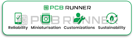
Have you ever wondered how PCBs (printed circuit boards) remain functional and are able to last long? The tiny copper traces on PCBs are well protected and do not corrode due to oxidation because of surface protection techniques. In this article, we will undertake a friendly, detailed exploration of PCB finishes, including what they are, their importance, and which might be most suitable for your project or learning.  

Why do PCBs require Surface Protection?  

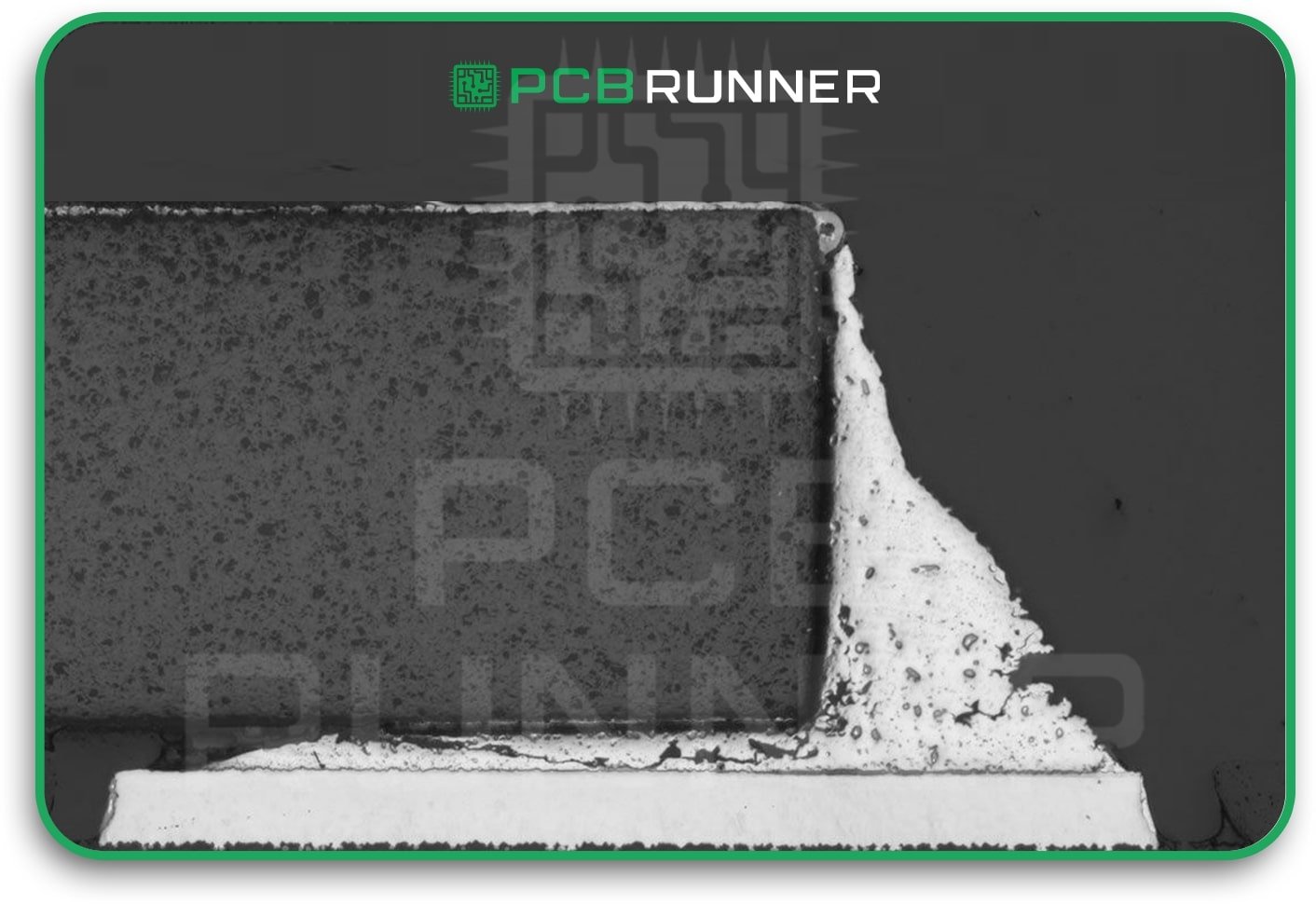
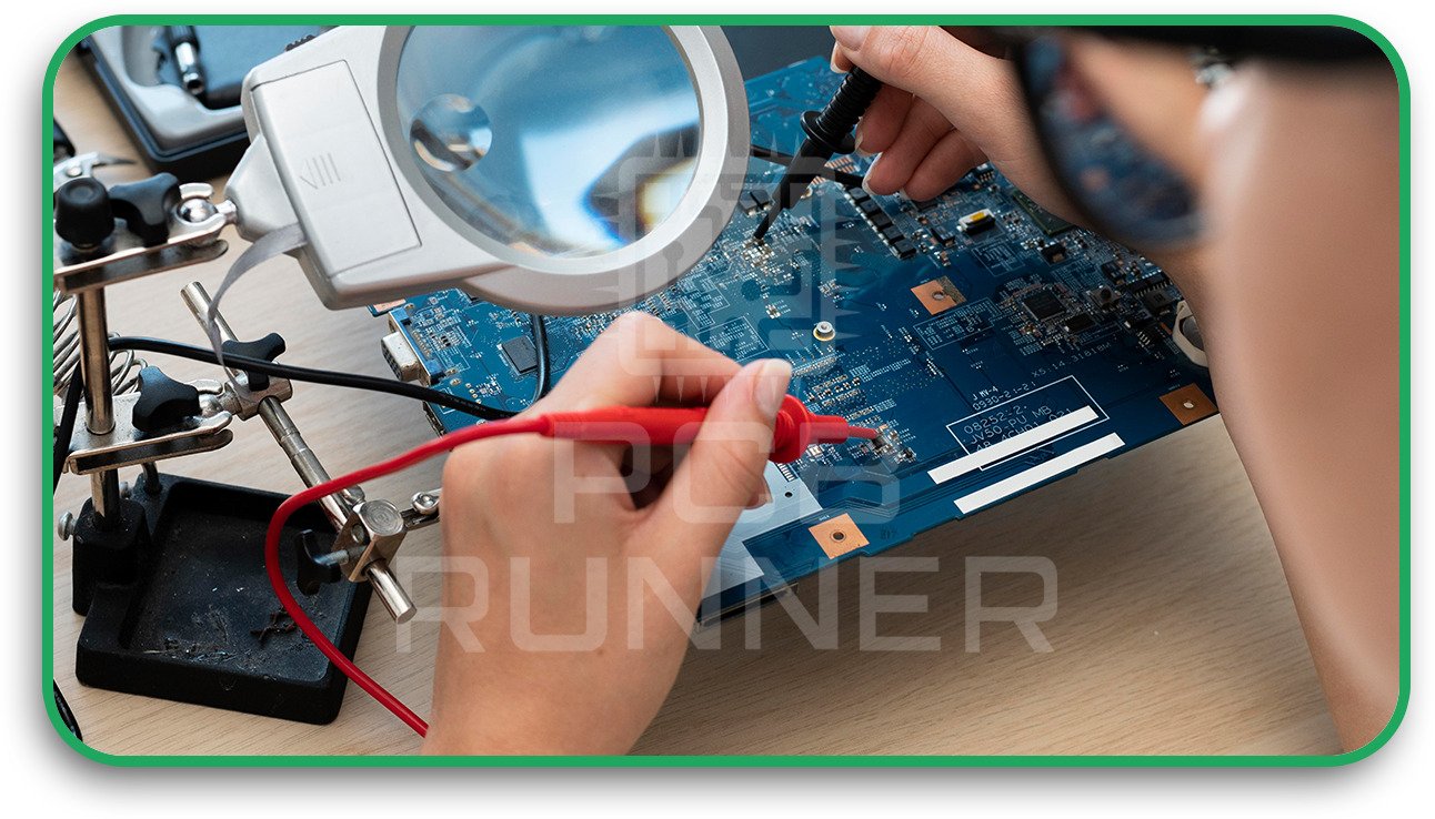
Think about baking cookies and leaving them exposed to the open air. In no time, they become hard and stale. PCBs also contain copper and thus undergo a baking-like process. During the CNC milling process, oxidised copper will be challenging to use, similar to brown and oxidised apples stuck turning brown, which creates problems during the PCB printed circuit board assembly, as well as the final steps of assembly.  

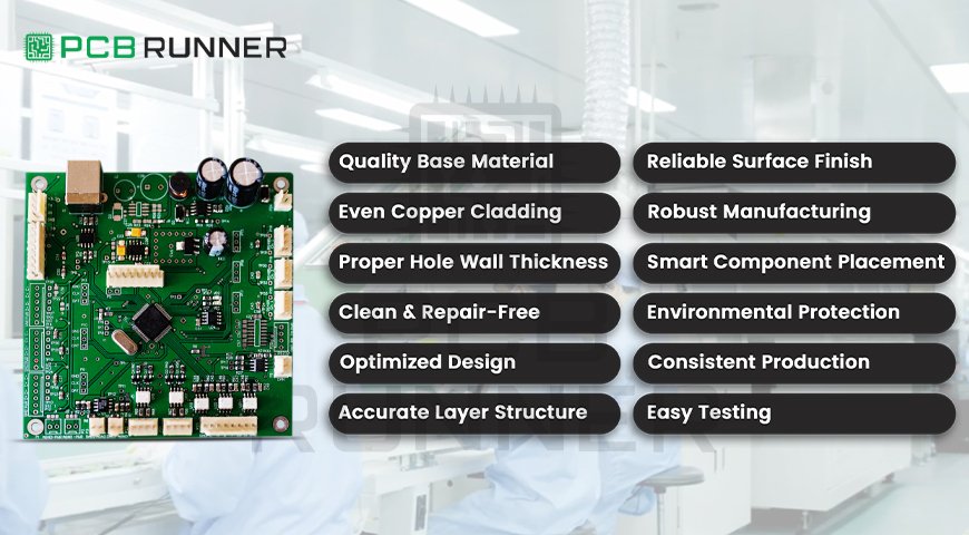
In order to make PCBs dependable and straightforward to assemble, manufacturers apply surface finishes or specialised coatings to PCBs, which reduce the chances of air, precipitation and other dangerous things, can severely damage their performance. Manufacturers try to use surface finishes that will add to the dependability of the PCBs.

How Does The Surface Finish Of A PCB Work?  

Think about if your school locker had a shiny sticker on it that prevents it from rusting. Surface finishes on PCBs help to prevent copper from oxidising, aid in the soldering of parts onto the board, and help in the overall working of the board.  

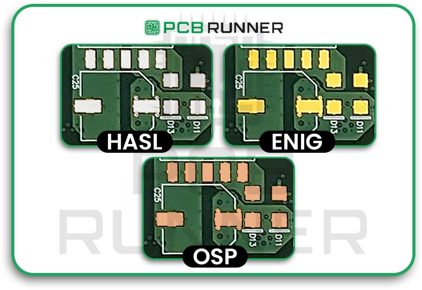
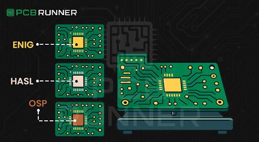
Three of the most common finishes you’ll hear about are ENIG, HASL, and OSP.  

Exploring The Main Types Of Surface Finishes Used On PCBs  

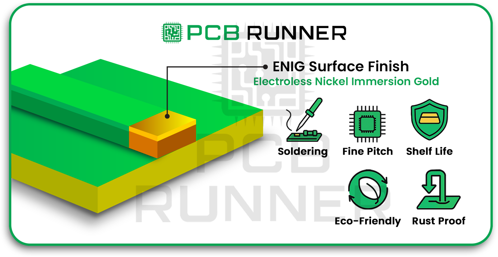
1. ENIG: Electroless Nickel Immersion Gold Surface Finish PCB  

The surface finish ENIG is a flat surface finish of nickel and gold that is shiny and helps to waterproof a PCB. The surface is flat and shiny while also being very reliable.

ENIG-Electroless-Nickel-Immersion-Gold-Surface-Finish-PCB

Benefits:  

  • Parts soldered to the PCB will remain attached through the entire building process.
  • Best for small spaces and parts, like in a smartphone and medical tools and equipment.
  • The gold surface delays any rust for months, and in some cases, even up to a year.
  • Good for the environment and products with strict safety standards.
  • Flexible and helps in rust resistance.

Drawbacks:

  • Cost: The finishing touch on a product with gold is prohibitive.
  • Not always needed: The gold finishing touch provides needless protection on simple boards.

When to choose it?

ENIG is a good choice when you want to augment the durability and longevity of the circuit board, also if you want to solder small parts while being concerned with the safety of the circuit board and the electronics.

2. HASL: Hot Air Solder Levelling PCB Surface Finish

HASL is an older but still proper technique. It is akin to a PCB being dunked into a bath of solder. The PCB is then soldered with hot air to smooth the finish. The finishing touch can be leaded or non-leaded.

HASL-Hot-Air-Solder-Levelling-PCB-Surface-Finish

Benefits:

  • Cost-effective: This is better for a project that needs to make and sell many boards.
  • Electronic components’ protection: The copper parts of the circuit board are covered in solder, preventing rust.
  • Error identification: The shiny sensor assists in looking for cracks and the mistakes that come along with it.
  • Embraced for a long time: This has been used widely in areas such as automotive, industrial and many more industries.

Drawbacks:

  • Not super smooth: The board’s surfaces, which have copper parts, can be covered in solder, preventing rust. Also, the copper components having a rough surface to them are not advantageous.
  • Non-leaded option isn’t eco-friendly: This has left a mark on the current eco-friendly approach that many companies aim towards.

When is HASL most suitable?  

For simple projects, bigger pieces, or when the budget is tight, HASL works best. PCB circuit board manufacturers typically prefer it due to its ease of application and consistency.  

3. OSP: Organic Solderability Preservative PCB Surface Finish  

OSP surface finish PCB applies a nearly invisible organic coating. It’s like applying an evident seal to your school books, protecting them from damage. 

 OSP Organic Solderability Preservative PCB Surface Finish

Advantages:  

  • Streamlined: Cheaper than using metallic finishes.  
  • Eco: Does not contain harsh chemicals or metals.  
  • Best for flat designs: The surface is even and smooth.  
  • Repairable: Parts can be unsoldered and re-soldered without much hassle.  

Disadvantages:  

  • Limited lifespan: Protects the copper for only 6–12 months.  
  • Risk of damage: Can be easily scratched with improper handling.  
  • Hard to check off: Because it’s clear, flaws become difficult to check.  

Best for:  

The best fit for projects needing faster assembly or low-cost outsourcing with a strong focus on saving money and eco-impact.

How Surface Finishes of a PCB Change Real-Life Projects

Imagine a student crafting a model volcano for a science fair. If he doesn’t waterproof the model, it will get easily destroyed. Surface finish protects printed circuit boards the same way finishing a model volcano protects it. It helps to prevent damage, wear, and finish wear and ensures the circuit board survives thorough testing as well as use.  

Whether it is computing, robotics, medical instruments, or toy designing, the relevant pcb surface finish will enable the device to perform optimally. This is precisely why engineers and PCB manufacturers put extra thought into every decision:

  • Durability: Will the board need to endure harsh conditions for years?  
  • Solderability: Are you using parts that are smaller for the smart gadgets?  
  • Cost/ Eco-friendliness: Is the project a school project, or is it a heavy-duty industrial device?  
  • Ease of assembly: Will they need to fix or solder the board again?  

Tips to help you choose the Right Surface Finish  

  • Check the complexity of the board: Small parts and intricate circuits call for the use of ENIG. Bigger and simpler components can use HASL or OSP.  
  • Keep the expense in mind: HASL is the next cheaper after OSP, and then ENIG.  
  • Think about the shelf life of your project: ENIG survives for the longest, and then HASL can survive for a few months. OSP survives the shortest.  
  • Think of these ENIG and OSP are eco-friendly, and they are prioritising the project directly helps the environment.
  • Inspectability: Inspection of HASL is straightforward and visually accessible, while OSP is challenging to see.

FAQs

If no finish is applied to a PCB, what is the most likely outcome, and what is the gloss and matte finish for the identical PCB?

The risk is the same as an insufficient protective coating. Heating and ignoring protective etiquette risks failure. Assembly failure is like the breakdown of a bicycle left outside to rust.

Which of the described finishes has the most extended operational life, and what is the 

difference between matte and gloss finishes?

Gloss finishes are generally valued for being visually appealing compared to matte. They are more prone to scratching, so their operational life will depend on the surface treatment of the substrate.

What do I do if a joint has to be reworked?

Finishes on OSP boards are the most permissive, and so they can be worked on repeatedly, allowing easy removal of the finish and addition of solder.

Easy Ways to Remember the Differences

  • ENIG: “Gold standard”—best for tiny, long-lasting boards.
  • HASL: “Budget pick”—classic, shiny, great for bigger, less-packed boards.
  • OSP: “Green choice”—cheap, environmentally kind, but not for use after a long shelf life.

Wrapping It Up  

In creating or configuring any device, safeguarding the PCB is as critical as deciding on its contours or the components it should house. Industry Standard Surface finishes ENIG, HASL, and OSP serve as the outer guard for the circuitry, making sure it is well protected, rugged, and ready for integration, regardless of what you intend to construct.  

Depending on your expectations, expenditures, and timeline, the finish selection varies. ENIG caters best to high-density and high-end boards, HASL is beneficial to generic works, and OSP is the cheapest of the three and environment friendly.  

The good thing is that knowing these protective methods enables you to engage meaningfully with PCB circuit board vendors or design and execute projects as a seasoned professional.  

Keep in mind, every PCB, regardless of the complexity, merits the right protective finish for its intended voyage. PCB Runner stands by this philosophy, ensuring each board, regardless of its dimensions, contributes to a bright, dependable, and safe future for electronics.


PCB Trace Width and Spacing Decisions

Essential Guidelines for PCB Trace Width and Spacing Decisions

Have you thought about the reasoning behind the differences in thickness among the copper lines on printed circuit boards (PCBs)? The thicker and thinner copper lines are referred to as PCB traces. Similar to the way roads in a city transport vehicles, traces on a PCB transport electrical signals. The thickness of these traces and the distance between them significantly influences the effectiveness of PCB design.

While the majority of you might not be deeply interested in electronics, PCB printed circuit board assembly, or the processes behind a circuit board supplier in the UK, you are likely to notice that there are design rules and restrictions that need to be observed during board construction. In this blog, we will explain these rules and design restrictions for you in a way that can be easily digested, even for a beginner.

PCB Trace Width and Spacing Decisions


Why Does PCB Trace Width Matter?

Consider a PCB trace to be a water pipe. A narrow pipe will not be able to transport water easily, similar to the way a narrow trace will impede the flow of electrical current due to resistant heat. Excess heat can damage the board.

For this reason, PCB designers order the current capacity of the PCB trace width before finalizing the width of the trace. Choosing the right trace width keeps the PCB functional and ensures all signals are processed efficiently.  

Key reasons why trace width matters:  

  • Heat control – For the efficient handling of current, wider traces are less prone to overheating.  
  • Signal quality – Correct trace width minimizes noise and interference.  
  • Durability – Damage to the copper during PCB production in the UK is minimized.  
  • Compliance – Manufacturing and safety standards are met.

PCB Trace Width Matter

What Is PCB Trace Spacing and Why Is It Important?  

As with roads, traces on a PCB require distance between lanes, which in this case is called trace spacing. If lanes are too closely spaced, vehicles may collide. On a PCB, with traces spaced too closely, electrical signals may “leak” between traces. This effect, called crosstalk, can lead to short circuits.  

Good spacing:  

  • Refrains from creating shorts and sparks between signals.  
  • Reduces interference between signals.  
  • Helps meet safety regulations for high-voltage designs.  

These spacing rules are determined largely by the voltage level and the PCB production method utilized in the UK.

How to Determine PCB Trace Width

There is no need to make estimations as there are tools such as a pcb trace width calculator which will do the job for you. These calculators take into consideration:

  • The Current (Amps) the trace will carry
  • The copper thickness on your board
  • The temperature rise you can allow

Take for example a 1 amp trace. With 1 ounce copper thickness, calculators will help you determine the width to keep it safe.  

Tip: Safety margins should be added. Wider traces will accommodate for surges just like wider roads which are better equipped for uncontrolled traffic increases

Determine PCB Trace Width

How to Decide PCB Trace Spacing 

As a rule of thumb, the amount of space is to do with voltage preventing a jump. The higher the voltage, the greater the distance.

There is a common standard:

  • Low voltage (<30V): 0.1 mm spacing is often fine.
  • Medium voltage (30V–100V): 0.6 mm or more.
  • High voltage (>100V): Several mm, always comply with safety standards.

Factors Affecting PCB Trace Width and Spacing

Every printed circuit board (PCB) is unique and requires specific factors to be considered when designing PCB traces. These include:  

Current Capacity  

A trace must be ‘wider’ to manage ‘more’ current.  

Copper Thickness  

A thicker copper layer is able to manage more current without overheating.  

Voltage Levels  

More spacing is required for higher voltages.  

Signal Type  

High-speed signals require careful width and spacing to avoid cross talk.  

Environmental Conditions  

Will the PCB be exposed to high temperatures or moisture? That requires wider traces and larger spacing.  

Factors Affecting PCB Trace Width and Spacing

Using PCB Trace Current Calculators  

A pcb trace current calculator is an important tool for firms to take the guess work out and ensure the design is functional. You input:  

  • Current Load
  • Copper Thickness
  • Maximum allowable temperature rise  

Common Mistakes in PCB Trace Design  

  • Narrow traces leading to overheating and damage.  
  • Ignoring spacing rules leading to short circuits or signals interfering with each other.  
  • Oversights such as sharp 90° corners or the extraction of manufactural limits weaken a board.

Prior to submitting your design for printed circuit board (PCB) assembly, ensure it is thoroughly checked for any possible mistakes.  

If you’d like expert design reviews before production, our engineers at PCB Runner can help you optimize your layout and avoid costly errors. Contact us at sales@pcbrunner.com to discuss your project.

Tips for Perfect PCB Trace Width and Spacing  

Designing and manufacturing printed circuit boards is a complex process, and faxing ensures success.  

  • Make sure to use a trace width calculator at the beginning of the design process.  
  • Make sure to check the manufacturer’s minimum trace width and spacing.  
  • Make sure the width of power traces is greater than the minimum.  
  • Make sure to keep high-speed signal traces both short and well-spaced.  
  • In order to reduce interference, keep analog and digital traces separate.  
  • Increase the clearance for high-voltage circuits.  
  • Always run DRC prior to production.  

Why These Decisions Matter for PCB Production in the UK  

When working with circuit board suppliers UK, providing accurate width and spacing details makes the manufacturing process smoother. It also ensures your design passes quality checks quickly.

Consequences of Neglecting Design Best Practices:

  • The board may encounter failures during the testing phase.
  • You may incur expensive redesign expenses.
  • There may be production delays.
  • Correct PCB trace width and spacing regulations save resources and finances.

Final Thoughts

While selecting the PCB trace width and spacing may seem trivial, it is the core of any dependable design. Be it a homemade pcb printed circuit board assembly or when collaborating with pcb production UK professionals, adhering to the guidelines will enhance the circuit’s durability and optimize its performance.

The positive aspect is that with the advancements of technology, guessing is now an obsolete practice. Smart and safe decisions can now be made utilizing trace width and current calculators, alongside IPC’s standards.

Use of IPC trace current and width calculators or CAD software will further support these decisions. While it is advisable to reach out to design professionals, manufacturers, and in this case, PCB Runner, who are grounded in production reality, can offer invaluable suggestions. Such collaborations will ensure the designs are realizable and align with production capabilities.

pcb runner

How the Stretchable PCB Technology Empowers the Future of Electronics

Have you ever wondered how electronic devices are able to bend, twist, or stretch without damage? Electronics are a critical part of our daily lives, including high-tech medical devices and smart fitness trackers. Stretchable PCB technology tackles this issue. Stretchable PCB technology marks a potential shift from traditional rigid printed circuit boards. This technology proves revolutionary as it permits circuits to stretch up to 200% of it’s length like a rubber band.

The goal of this article is to provide a more detailed overview of stretchable PCBs and how it’s using today’s technology to innovate the electronics of tomorrow.

What a Printed Board Stretchable Circuits

With today’s advanced technology, stretchable printed circuit boards (PCBs) are revolutionising circuitry by using new materials and designs that allow them to bend and twist. Unlike PCBs, which are rigid, stretchable PCBs have the ability to stretch, twist, and bend over 200% of it’s length without malfunctioning.

These PCBs are created using elastic materials along with specific designs, for example, serpentines (wavy lines), which ensure the stretching is distributed evenly across the circuit and no single point is overly stressed and damaged. This characteristic makes them especially helpful in applications where devices have to move or change shape frequently.

Stretchable Circuits

How does the technology for stretchable PCBs work?

The materials and the designs both have to work in tandem for stretchable PCB technology to function, especially:

  • Elastic Substrates: Rubbery materials such as silicones or specific polymers, which are soft and flexible, are known to stretch and not tear.
  • Serpentine Copper Traces: The copper lines that transport current are not composed of straight lines; instead, they wiggle in snake-like shapes. Snake-like copper lines are able to stretch and loosen without breaking.
  • Durable polyethene biosystem: This lays emphasis on the rings of the utilised materials, which are safe for the usage of wearing on skin or even fine for surgical implants.

Durability: Thus, PCBs are very reliable in the regard that they may be stretched several thousand times without any loss of function.

stretchable PCBs work

Flex PCB Fabrication and Rigid-Flex Boards

The older stretchable PCBs utilised Flex PCB fabrication or rigid-flex boards. The elderly boards with rigid-flex boards are made from rigid and flexible parts, meant to allow some movement, though overall limited:

  • Flex PCBs are bendable, though they restrict stretching.
  • Combining solid sections that hold maximum stability with flexible sections results in rigid-flex boards that are not stretchable.

Flex PCBs already enable wearables and high-movement electronics. Stretchable flex PCBs take this further by permitting real stretchability, all while ensuring reliability, which deepens possibilities within wearables and other high-movement electronics.  

Where Can Stretchable PCB Technologies Be Applied?  

Stretchable PCBs, Crosswear Ergonomics, and Advanced Materials Creatively:  

  • Wearable Electronics: Smart clothing and health monitors must expand and contract seamlessly. Stretchable PCBs seamlessly support dynamic movements.  
  • Medical Devices: Stretchable PCBs are integral to devices like skin patches, monitoring heart rate, and neural interfaces that wrap around nerves to ensure proper function while allowing user comfort.  
  • Robotics: Soft robots require stretchable PCBs to provide suitable circuits for motion-responsive sensor skins and joints.  
  • Consumer Electronics: Stretchable circuits in new foldable phones and curved screens enable these devices to function even when bent or folded.  
  • Automotive: Stretchable PCBs are essential for sensors in car seats and dashboards that flex with the interior contours.  

All these disciplines gain from the capability to design electronics, not only offering flexibility, but also the ability to stretch and adapt to real-world dynamic shapes.

What Makes Stretchable PCB Technology Essential?

Known electronics can be bulky and rigid, which is a problem for some modern devices. Designers of devices and equipment no longer face rigid boundaries concerning the form of a circuit board with the advent of stretchable printed circuit technology. This signifies:

  • Enhanced Comfort: Wearable gadgets and devices will be more comfortable as they will naturally move along with the body.
  • Improved Durability: Devices will be able to endure repeated bending and stretching without sustaining damage.
  • Advanced Electronics: Devices can be embedded into garments, soft medical implants, or the skins of robots.
  • Enhanced Effectiveness: Even with stretching or twisting, the accuracy of the sensors and components is retained.

What Are the Issues?

Despite the fantastic capabilities of stretchable PCBs, they do pose a few unique challenges:

  • Specialised materials and careful designs to ensure the circuit’s integrity while stretching make fabrication complex.
  • Regular PCBs tend to be more affordable as compared to these materials and designs.
  • Extreme repetitive stretch or harsh environment testing of the devices is critical.
  • As stretchable PCB technology matures and more manufacturers focus on investment, the unique challenges are bound to lessen.

How to Pick the Optimal PCB Technology  

For designers working on stretchable circuits, these points should be noted:  

  • Know how your device moves: Will it be bending, twisting, or stretching? Only stretchable PCB technology works for devices that absolutely need to stretch.  
  • Analyse the biocompatible option: encapsulation and elastic substrates differ in a wide range for various uses. Consider the medical devices that need such materials.  
  • Work with PCB producers who have vast experience in flexible and stretchable PCB production.  
  • Blend in rigid-flex board designs in portions that require stretchable and flexible elasticity.  
  • Conduct durability and electrical performance tests on the prototypes.  

Stretchable PCBs and the Future of Electronics  

Stretchable PCB technology is making it possible to create extraordinary new devices as electronics shrink and become smarter. Think of medical patches that continuously monitor health stats invisibly, or sensor-laden smart fabrics that change colours in reaction to the wearer’s movements.  

Those boundaries continue to be pushed for stretchable printed circuit boards as researchers find ways to make them stretch even more and for longer. These printed circuits are essential for the Internet of Things, or IoT, as the smart devices need to be well integrated into daily activities.

Conclusion

The stretchable PCB technology serves more than just a purpose; it’s a unique gift of modern engineering that facilitates the flexing of the newest electronic devices. Stretchable circuits improve the functionality of devices in the medical field, robotics, and many other gadgets, making devices smarter and more durable.


Most people are concerned with electronic design and technology innovation, and for them, embracing stretchable PCB technology will be a must for adoption.

At PCB Runner, we help by making these innovations known to designers, engineers, and technology lovers, and in the process, they understand the innovations and stay prepared for the upcoming challenges and innovations.

pcb runner cover

Step-by-Step Guide to Medical PCB Design for Medical Devices

Designing electronics for healthcare is unlike creating boards for consumer gadgets. A single failure can compromise patient safety or lead to costly regulatory delays. This guide walks you through a proven, end-to-end process for medical device PCB design from concept to production by ensuring compliance and reliability.

Whether you’re comparing printed circuit board manufacturers, seeking custom PCB assembly, or planning a full turnkey assembly for high-stakes medical equipment, these steps will help you meet strict quality standards and reduce time to market.
And if you need expert support at any stage, our team is here at sales@pcbrunner.com  to help you move from design to production with confidence.

Let’s start with a question.

If you were designing a medical device, something that a patient’s life might depend on, how much room would you leave for error?

Probably none.

That’s the reality when working with medical device PCB design. These boards go into equipment like heart monitors, defibrillators, MRI scanners, and portable diagnostic tools. In all those cases, failure isn’t just inconvenient. It could be dangerous.

Here’s the thing: designing a PCB for medical devices is not the same as designing one for a smartphone or a smart home gadget. The technical side is more demanding. The regulations are tighter. The margin for error? Almost zero.

So let’s walk through the process step-by-step, from the first sketch to the point where the board is ready to be assembled and tested. I’ll keep it simple, clear, and practical so that you can use this as a real checklist, not just another “how-to” you forget five minutes later.

steps

Step 1: Draw the Schematic

Every board starts with a schematic. Think of it as your map showing how each component connects.

When you’re creating a schematic for PCB assembly for medical purposes, you want to include key details right from the start:

  • The material type you expect to use for the PCB.
  • The power needed for your design.
  • All essential components, placed and connected logically.

Don’t rush this part. Mistakes here will haunt you later in the layout stage, and fixing them later costs time and money.

Schematic

Step 2: Design the PCB Layout

Once you have the schematic, you move to the layout stage. This is where you decide where each component physically sits and how the copper traces connect them.

Most designers use CAD software for this. You’ll import your schematic, then start arranging components in a way that keeps signal paths short and clean.

For medical device PCB assembly, noise and signal clarity are critical. That means:

  • Avoid routing high-speed signals near sensitive analogue lines.
  • Keep critical signals short.

Plan your ground and power planes early to avoid last-minute patch jobs.

PCB-Layout

Step 3: Pay Attention to Critical Medical PCB Factors

This is where many engineers miss details that matter in regulated industries.

Here’s what you should focus on:

  • Component choice: Stick to parts that have proven long-term reliability. Don’t gamble on untested suppliers.
  • Split power planes and proper grounding: Splitting power planes and adding multiple ground layers helps reduce interference.
  • Clear silkscreen markings: Make component labels unambiguous so assembly teams can find precisely what goes where.
  • Signal-to-noise ratios: Medical devices often deal with very low, sensitive signals. Noise on those lines can cause incorrect readings or insufficient data.

If you get just one thing from this section, let it be this: in medical electronics, stability is everything.

Step 4: Review the Bill of Materials (BOM)

The BOM is your recipe for building the board. In medical device PCB design, it’s also part of your compliance record.

What to do here:

  • Confirm every part number and supplier is correct.
  • Read each datasheet, don’t assume a part will work because it looks right.
  • Create an alternate component list in case your first-choice parts are unavailable.

A complete, accurate BOM speeds up full turnkey assembly because there’s no back-and-forth with the manufacturer on missing or mismatched components.

Bom

Step 5: Create an Assembly Drawing

The assembly drawing shows exactly how your finished board should be built.

Think of the assembly drawing as the instruction manual for your custom PCB assembly team. It should include:

  • Component outlines and reference numbers.
  • Polarity markings were required.
  • Notes about special handling or soldering requirements.

A good assembly drawing removes guesswork and ensures that every medical device PCB assembly looks and works the same.

Step 6: Add Test Points

Testing is non-negotiable in medical electronics.

Adding clear, accessible test points during design helps technicians check voltages, signals, and performance without damaging the board. This improves test speed, reduces errors, and makes future troubleshooting easier.

Skipping test points is one of the most common mistakes in PCB design, and one of the costliest to fix later.

Step 7: Work Closely with Your Manufacturer

Here’s what this really means: pick your printed circuit board manufacturers UK partner early, and involve them in the design process.

Why? Because a manufacturer experienced in PCB assembly for medical devices will:

  • Suggest better materials that meet medical compliance.
  • Flag design features that might raise costs or cause delays.
  • Help with documentation for ISO 13485 requirements.

A good medical device PCB isn’t just designed well, it’s also built by people who understand the regulations and demands of healthcare electronics.

Step 8: Meet Regulatory and Quality Documentation Needs

You can’t sell a medical device without paperwork, especially in the UK, EU, or US.

At a minimum, expect to prepare:

  • Design history and change records.
  • Traceability logs for all components.
  • Test records and inspection reports.
  • Verification/validation documentation.

An experienced manufacturer offering a complete turnkey assembly can help generate and store these records for you.

Step 9: Prototype and Test Thoroughly

Never jump into mass production without building prototypes first.

Prototypes let you:

  • Verify your schematic logic.
  • Catch signal integrity issues.
  • Confirm heat dissipation is adequate.
  • Validate assembly instructions and BOM accuracy.

With medical device PCB assembly, multiple prototype rounds aren’t overkill, they’re a smart investment.

Step 10: Move to Production with Full Turnkey Assembly

When the design is solid and testing is complete, it’s time for production.

Choosing a full turnkey assembly streamlines things. It means the manufacturer handles:

  • Board fabrication.
  • Component sourcing.
  • PCB assembly.
  • Testing and inspection.
  • Final packaging.

This approach saves time and keeps the process consistent, which is crucial for PCBs for medical devices.

Step 11: Focus on Long-Term Reliability

Remember, many medical devices run for years without interruption. That means your PCB must be durable enough to handle long service cycles, cleaning cycles, possible heat stress, and occasional mishandling.

Ask your manufacturer about:

  • Conformal coating for moisture protection.
  • High-reliability solder joints.
  • Specialised component mounting for vibration resistance.

Why the Right Partner Matters

Choosing the wrong manufacturer can lead to delays, compliance issues, or even device failures. That’s why partnering with PCB Runner is critical. We specialize in custom PCB assembly for high-stakes industries like medical devices, offering complete turnkey solutions that meet the strictest quality standards. Get in touch with our team today to ensure your medical device PCBs are built with precision, compliance, and reliability from the start.

Working with the wrong manufacturer can cause delays, compliance failures, or worse, device malfunctions. Companies like PCB Runner focus on custom PCB assembly for precisely these high-stakes situations.

They understand the nuances of medical device PCB design, provide complete turnkey assembly, and ensure that every PCB for medical devices meets strict quality standards.

Wrapping It Up

Designing a medical device PCB isn’t just electrical engineering. It’s a careful mix of technical precision, regulatory compliance, and practical assembly planning.

Get the schematic right. Plan your layout to minimise noise. Double-check the BOM. Add test points. Work with a manufacturer who understands the regulatory side as well as the engineering.

Do that, and your medical device PCB assembly will be ready to perform exactly as needed, every time.

And once the boards are built, don’t overlook professional labelling. Partnering with a supplier like Dura Fast Label helps ensure your finished device looks as professional as it performs, with labels that last through use, cleaning, and transport.

If you follow this step-by-step guide, you’ll not only meet the technical and legal requirements for medical PCBs, you’ll also end up with a design you can trust, and so can your end users.

That’s the real goal.

pcb-hardware-debugging

Effective Troubleshooting Techniques for PCB Hardware Debugging

Almost all electronic devices today use a printed circuit board (PCB). Unfortunately, a printed circuit board that is carefully designed and assembled may sometimes malfunction. At this junction, you may have to employ PCB troubleshooting techniques to repair and resolve issues in the shortest time possible. This is especially the case while working on prototypes or bulk orders from trusted assembly manufacturers. Knowing how to debug your PCB is critical in this case.

In this blog, we will highlight the problems associated with PCBs and the solutions that anyone can perform. Methods and tools will be discussed, ranging from basic visual inspections to complex electrical tests. You will learn to diagnose numerous issues and how to isolate problems. Whether you are a beginner or have some experience, these techniques will enable you to resolve circuit board issues more efficiently.

What Is PCB Troubleshooting?

Troubleshooting printed circuit boards, or PCB troubleshooting, is the process of identifying and removing issues that prevent a printed circuit board from functioning accurately. This is often the case after receiving the assembled board, whereby several faults may be present. For instance, the circuit may fail to power on, some components may fail to respond, or some signals may act abnormally.

Every problem requires a definite order of actions to solve it. Start with basic things first before moving on to more complex things. Imagine a detective trying to solve a case; you need to piece together clues to resolve the problem at hand. 

PCB Troubleshooting

Why is it Important to Solve Troubleshooting Issues on PCBs?  

  • Saves time and money: Notice issues early on to avoid expensive redesigns or recalls of the product.  
  • Ensures product quality: The ability to troubleshoot enhances the reliability of electronic products.
  • Speed up prototyping: Working on a PCB prototype comes with a lot of issues that need to be resolved rapidly.  
  • Supports complete turnkey assembly: When you order from circuit board suppliers in the UK & Europe, understanding troubleshooting helps to assure the quality of the order.  
  • Deepen understanding: troubleshooting builds a stronger grasp on how the circuit operates and aids future projects. 

Troubleshooting Issues on PCBs

Common Issues Found on PCB Troubleshooting  

Before attempting to solve issues, it is essential to be aware of the faults you might come across:  

  • Open circuits: Paths that are straight but broken.  
  • Short circuits: Unwanted connections that alter the typical passage of current.  
  • Wrong placement of components: Parts that are installed on the wrong pads or orientation that is flipped.  
  • Cold solder joints: Weak connections due to poor soldering.  
  • Burnt components: Damaged parts that are considered faulty.  
  • Faults in power supply: Voltage drops or instability in power rails.  
  • Integrity issues with signals: Distortion and noise due to poor wiring.  
  • Firmware or software bugs: Issues that are caused due to coding on the board.

At pcbrunner, we minimize these troubleshooting headaches by applying strict manufacturing controls, thorough testing, and design-for-manufacturing reviews so your boards work as intended from the start.

Essential Gadgets Needed for PCB Hardware Debugging

You don’t want to purchase a whole lab setup to get started. Initially, having a few tools is enough and can be expanded upon:  

  • Multimeter: Measures voltage, resistance, and continuity.  
  • Oscilloscope: Used to view waveforms and their shapes.  
  • Magnifying glass or USB microscope: For a magnified view of microscopes and solder joints.  
  • Power supply with current limiting: Used to power a board with a low risk of damage.  
  • Logic analyzer: Used for checking and decoding complex digital signals.  
  • Thermal camera/ IR thermometer: Used to detect components that possibly overheat.  
  • Tweezers and small tools: Tools used to hold small parts that require magnification to be seen.  

Block-by-Block Steps on PCB Troubleshooting Techniques  

1.  Start by looking closely  

Most PCB problems arise from easily overlooked issues. Here are a few of them:  

  • Broken or lifted traces: Looking for marks and scratches on copper with a magnifying glass.  
  • Solder bridges: Pops of solder that are adjacent and blobbed along with solder.  
  • Cold solder joints: Joints that are connected by solder that is dull or cracked.  
  • Foreign debris: Shorts caused by dust and metal that is unwanted.  
  • Overheat burn: Looking for signs of damage or things that are overworked and burned.

Finding and fixing problems visually saves time and effort down the road.  

2. Basic Tasks with a Multimeter  

Your multimeter can also come in handy for simple tasks with electricity:  

  • Continuity test: Make sure the two points that should be connected are connected. A multimeter that beeps indicates a connection. These tests help for open and short circuits.  
  • Resistance measurement: Test suspicious points to see if there is low or high resistance.  
  • Voltage measurement: Carefully power the board and measure key components and essential rails to check for supply voltages.  

Before complex tools are needed, you can focus on problem areas using a multimeter.  

3. Cautiously Observe While Powering Up  

It is essential to carefully power the board as it may be damaged due to existing faults. Follow these suggestions:  

  • Employ a current-limited power supply to help prevent burnouts.  
  • Pay attention to anything unusual that may overheat.  
  • Listen and smell for burning, which indicates shorts and failed components.  
  • Use LEDs or test points to determine if critical areas are powered.  

This step should never be rushed, as sometimes, due to a power issue, several faults tend to be caused that cascade.

4. Focusing on Signal Checking with an Oscilloscope

If functionality appears to be off, check signal waveforms:

  • Are the voltage levels at the expected places?
  • Is the timing correct? (rise and fall times)
  • Is there signal noise or ringing?
  • Use triggers to capture transient mistakes.
  • Using oscilloscopes allows you to validate the logic, confirming that he made the proper validations that were needed while working on the PCB.  

5. Reviewing the Digital Signals with the Logic Analyzer

In cases where the board has I2C or SPI or UART, the board contains I2C or SPI boards, the board necessitates the use of logic analyzers, hence we:  

  • Capture multiple signals and do it at the same time.
  • Decode the communication made.
  • Detect or measure the timing and any data errors.

This is vital and fundamental for the use of microprocessors during the testing of the PCB prototype.  

6. Examine and Restyle the Solder Joints  

In the presence of bad solder joints, there is always the use of:

  • The use of a soldering iron to reflow the joints.
  • Use of a solder wick to get rid of bridges.
  • And, the use of flux enables the solder process to flow better.  
  • Good joints remain vital in the electronics domain and correct undead devices as per the working.

7. Software and Firmware Examination  

In the presence of PCBs having programmable devices:  

  • Confirm if the firmware has been flashed the right way.
  • Confirm the correct way with debugging tools while processing the code.
  • Confirm the running of the software with good hardware to know the defects.  

In some cases, it is the software that causes the entire facade of the hardware failures.

Tips for PCB Troubleshooting Success

  • Document everything: Capture notes and take photos during the debugging for future reference.
  • Divide and conquer: Take problems on the board in sections so as to lessen the workload.
  • Stay organized: Maintain a neat work area that is well-lit, has all the required tools.

Contact our sales engineer at sales@pcbrunner.com to discuss design goals, get a production estimate or explore how our pcb prototype expertise can streamline your next build.

Conclusion

Troubleshooting a PCB does not have to be a stressful experience. Follow the steps of inspection, measurement, powering the device, and analyzing signals, and you will be able to fix most of the hardware issues.

Here at PCB Runner, we maintain a high standard of quality from prototyping to full production. However, knowing the PCB troubleshooting tips provided will help you get the most out of your boards, no matter what stage you are at.

Embedding Components in Printed Circuit Boards

Key Techniques for Embedding Components in Printed Circuit Boards

Designing  custom printed circuit boards for today’s compact, high-speed electronics requires more than just traditional surface mountain. Engineers face shrinking form factors, heat management challenges, and signal-integrity issues. Embedding components inside the board itself addresses these constraints.

The printed circuit boards are the brains of any modern device. When designing or fabricating a custom printed circuit board, integrating components into the board can be more efficient with regard to area, performance, and reliability.

This blog outlines the techniques of embedding components into PCBs. 

Embedding Components

Methods of Integrating embedded components into printed circuit boards

Printed circuit boards traditionally mount parts on the surface. But embedding changes the game. In a custom printed circuit board or DI printed circuit board, passive parts and even ICs can be laminated inside the stack.

Embedding:

  • Enhances the complexity of the design and the density of the layout without enlarging the board.
  • Shields components from mechanical wear, dust, and damage.
  • Shortens signal pats, improving accuracy and speed.
  • Enables the development of lighter, smaller, and more reliable devices.

The trend of miniaturization is more noticeable with advanced printed circuit boards, like HDI printed circuit boards or specialized ones.

Embedding

Benefits of Embedding Components

The advantages of embedding components on a circuit board are the following:  

  • Space Saving: Embedding either increases the surface area within the circuit board for the addition of other parts or reduces the surface area of the PCB overall. This is crucial for wearable electronics.
  • Enhanced electrical performance: Internal component placement reduces parasitic effects as well as signal interference when compared to external component mounting. This increases accuracy and speed.  
  • Greater reliability: Parts that are embedded are more reliable when it comes to protecting against mechanical shocks, dust, or corrosion.  
  • Reduced soldering steps: Embedding cuts the number of solder joints and placements, lowering assembly errors and shortening production time.  
  • Some embedded approaches enhance the dissipation of heat, which improves thermal management.  

At pcbrunner, we specialize in PCB embedding solutions that bring all these advantages into your design.

Key Approaches to Embedding Components in PCBs

There are other approaches to the embedding of components in printed circuit boards, other than the component placement:  

Creating Cavities or Slots in PCB Layers

This approach is cavity embedding:  

The precision cavity approach involves the machining or laser drilling of the recesses into the PCB layer. This technique is often referred to as cavity embedding.  

Chips or components are placed into the recesses so that they are flush or below the layer surface.  

The parts are secured to the recesses using adhesives.  

Subsequent layers of prepreg or a core layer are added to the initial layers to seal and build the stacked PCB.  

This technique is mainly applied in the embedding of passive components such as resistors and capacitors, as well as thin IC packages. They enable better integration without the addition of surface board thickness.

2. Sandwiching Parts Between Prepreg Layers

Prepreg materials are crucial in PCB lamination. Manufacturers:  

* Position components between sheets of prepreg (semi-cured resin sheets).

* Stack several prepreg and core layers containing parts within them.  

* Heat and apply pressure to cure the stack to create a single, solid, bonded piece.  

This method effectively incorporates both active and passive components. It is essential to control material thickness to avoid warping the board.  

3. Via Connections and Laser Drilling

The rest of the board requires electrically connecting the embedded parts. Laser micro-drilled vias do the following:  

* Drilled access holes to reach pads on the embedded components.

* Currently used to conduct the vias with copper electrically.  

* Attach embedded components directly and eliminate the need for long traces.  

This is especially important in HDI printed circuit boards for the backbone of connecting hidden components in restricted spaces using laser via technology.  

4. Embedding with Film

Thin substrate materials are transformed into flexible ones using:  

* Thin polymer films are used to place components on.

* Films are then incorporated into multilayer PCBs.  

This is important for flexible and bendable PCBs where there are no rigid cavities.

5. Additive and 3D Printing Techniques (Emerging)

A few manufacturers are looking into 3D printing and additive manufacturing for embedding:

The addition and layering of particular conductive and insulating materials.

There are mid-process component integrations.

While they are still in the experimental phase, this could enable incorporating more intricate designs with different geometries.

Prototyping Considerations for PCB Prototypes with Embedded Components

Before moving to mass production, it’s a smart idea to build at least one PCB prototype with the planned embedded components. Working closely with your PCB supplier early on helps you to understand key process limits like how deep cavities can go, the tolerances for laser-drilled vias, and the thickness of prepreg materials. By adjusting your design to fit within these limits, you can avoid expensive rework later and get your product to market faster.If you’d like expert support with prototyping or need clarity on design tolerances, our team is here to guide you through every step before mass production to contact our sales engineer contact us today at sales@pcbrunner.com

Tips for Designing with Embedded Components –

Get the order right for cavity and embedded components placement: The PCB thickness and spacings between layers to be mounted must be considered.  

  • Don’t overly restrict space for routing: Space for routing and connections must be available for laser-drilled fine vias.
  • Consult with the suppliers: Component embedding feasibility can be confirmed with suppliers.
  • Respect weak zone distances: Minimum distances around embedded components are short, weak zones, or damaging structural integrity.

What are the Impacts of Embedding on the PCB Fabrication and Assembly Processes? 

The addition of components that embed firmly changes the entire PCB production life cycle:

  • Fabrication complexity: undergoes changes with layering precision, requires specialized equipment (laser drills), and careful pre-cured board stacking for uniform board thickness.
  • Blind and active inspection: embedded components require specialized X-ray inspection methods for verification of placement and connection for the part hidden in the layers.
  • Assembly: the surface-mount assembly stage is less. But requires high-level precision in PCB layout to ensure that all embedded components interface appropriately with via nets. Embedded components must withstand the temperature and pressure of lamination.
  • Cost: Embedding parts increases the cost. But, in most cases, production cost and time are reduced, and the entire system size and intricacy are increased.

HDI Printed Circuit Boards and Embedding 

Mobile and aerospace industries utilize HDI (High Density Interconnection) PCBs. They are embedding-enhanced for increased efficiency:

  • Incorporating passive components into HDI stackups helps to reduce the number of board layers.
  • Permits the use of small microvias and laser-etched cavities to densely pack functions.
  • Increases signal integrity and improves reliability for high-speed designs.

Conclusion

Integrating components into printed circuit boards eliminates several steps in the processes of miniaturizing and accelerating the efficiency of electronic devices. Manufacturers are able to make custom printed circuit boards and HDI printed circuit boards using advanced techniques like cavity creation, prepreg lamination, and laser via truly remarkable connections.  

Whether you are designing a PCB prototype or strategizing for large-scale production to know how embedding techniques interact with circuit board components. For further guidance, reach out to PCB Runner.  

Printed Circuit Boards

Essential Features of Reliable Printed Circuit Boards

All modern electronics depend on printed circuit boards (PCBs). Your PCB needs to perform effectively and last a long time, whether you’re constructing a simple gadget or a medical device that could save your life. But what makes a PCB work well? In this blog, we’ll discuss the most critical aspects of a high-reliability PCB. We’ll also discuss what to look out for when printing PCBs and creating prototypes, as well as how to ensure your PCB printed circuit board assembly lasts. We’ll use short sentences and basic vocabulary so that everyone can understand.

Why PCB Reliability Is Important

A well-designed PCB ensures your product operates safely and smoothly. The entire gadget can stop functioning if a PCB fails. This could be problematic in certain situations, such as with automobiles or medical equipment. That’s why it’s so crucial to design very reliable PCBs. You don’t want to put your goods or your name on the line.

1. Good base materials

Choosing the correct materials is the first step in constructing a sturdy PCB. Fibreglass, ceramic, or polyimide are common materials for the base, or substrate. The board can handle heat, stress, and chemicals better with good materials. The board can break or stop working if the base isn’t strong.

Always use high-quality, tested materials for your PCB. This helps prevent issues like delamination or open circuits.

materials

2. Copper cladding that is thick and even

Copper is utilised on the board to send signals and power. The copper layer must be thick enough and meet international standards, such as IPC-4101 Class B/L, for a PCB to be reliable. This helps maintain the insulation (dielectric) layer at the correct thickness, resolving performance issues.

Make sure the copper covering on your PCB meets or exceeds industry standards.

Copper cladding


3. The right thickness of the hole wall

To link different layers, holes in the PCB are employed. Copper, which is usually at least 25 microns thick, covers the interior walls of these holes. This keeps the board from getting larger and maintains strong connections, even when they are under stress.

The main point is that thick hole walls make the board stronger and prevent cracks or breaks from occurring when it’s being assembled or in use.

right thickness of the hole wall

4. No solder repairs and cleanliness

A PCB that is clean is a dependable one. Dust, debris, or residual solder can cause faulty connections or shorts. High-reliability boards are cleaned with great care and rarely require repair with solder or replacement of damaged lines. Solder fixes can cover weak places that could break later.

Ensure the boards are clean and have no damage. This makes it less likely that something will go wrong.

No solder repairs and cleanliness

5. Optimised PCB Design 

Planning your layout carefully is essential for high-reliability PCB design. Avoid using sharp edges, ensure traces are short, and use wide traces for power lines. If necessary, add more copper or heat sinks to your design to enhance its performance. The board will continue to function even if one part fails, as it has redundant connections and sophisticated trace routing.

A good design keeps your signals strong and your board cool.

Optimised PCB Design

6. Correct Layer Structure

Many PCBs feature more than one layer. How you arrange these layers is essential. Multilayer boards can handle more connections and produce less noise, but they are more challenging to assemble. Blind or buried vias (holes that don’t extend all the way through) can make the board more reliable and occupy less space.

Select the appropriate number of layers and the most suitable types of vias for your specific needs.

Correct Layer Structure

7. Good finish on the surface

The polish on the surface protects the copper and makes it easier to solder. HASL, ENIG, and OSP are some of the most common finishes. There are both good and bad aspects to each. The right coating makes it easier to solder and protects the board from rust.

Select a surface finish that complements the way you assemble the pieces and how the board will be used.

Good finish on the surface

8. Strong Manufacturing and Testing

A good factory makes a reliable PCB. Find PCB printing and PCB prototype services that examine the quality of their work at every stage. Advanced factories utilise laser drilling, optical inspection, and electrical testing to identify faults before they escalate. They also check boards for humidity, heat, and vibration.

Select makers that thoroughly inspect and test every board.

Strong Manufacturing and Testing

9. Choosing and placing parts carefully

If the parts are defective or assembled incorrectly, even the greatest board will fail. Get your parts from providers you can trust. Put the parts in a place where they can cool and be soldered easily. Don’t crowd, and ensure everything is in its proper place.

Good parts and sensible placement make it easier and more reliable to put things together.

placing parts carefully

10. Protecting the environment

Some boards must operate in environments that are hot, cold, damp, or prone to vibration. These boards must be made of specific materials or have special coatings. If needed, add protection against electromagnetic noise and static electricity.

Make plans for the real world where your board will be used.

Protecting the environment

11. Consistent Production

It should be straightforward to create reliable PCBs repeatedly. Utilise existing ideas and collaborate with established manufacturers. This makes it easier to resolve problems when they arise and maintains high quality.

The main argument is that standard designs and methods lead to fewer surprises and better boards.

Consistent Production

12. Simple to Test

It’s straightforward to test reliable boards. Place test points and clearly label your board so you can examine it both before and after assembly. This helps you detect and fix problems before they get to your consumer.

Include testing in your design from the beginning.

Testing and Quality Assurance

Critical Features for High Reliability PCB

Feature Why It Matters
High-quality materials Handles heat, stress, and chemicals
Thick copper cladding Strong signals and power, fewer failures
Proper hole wall thickness Strong connections between layers
Clean, repair-free boards No hidden weak spots or dirt
Optimized design Less noise, better heat control
Correct layer structure More connections, less noise
Good surface finish Easier soldering, less corrosion
Strong manufacturing/testing Catches problems early, ensures quality
Careful component selection Reliable parts, easier assembly
Environmental protection Survives tough conditions
Consistent producibility Reliable boards, batch after batch
Easy testability Find and fix problems quickly

Why PCB Runner Cares About Dependability

We at PCB Runner realise that every device needs its PCB to work. That’s why we pay attention to every step, from printing the PCB and creating the prototype to assembling it and testing it. We only use the highest-quality materials, adhere to strict guidelines, and meticulously inspect the quality of every board. PCB Runner is a partner that prioritises high-reliability PCB design and all the key aspects of high-reliability PCBs. Every time, your boards will function better, endure longer, and help your products thrive. 

Smarter Manufacturing with All-in-One Assembly Services

Smarter Manufacturing with All-in-One Assembly Services

It’s not enough to just make a circuit board to make electronics today. It’s about bringing together all the phases, from design to final testing, so your product works and reaches the market quickly. That’s where all-in-one assembly services come in. They do everything, from making PCBs to sourcing parts and assembling them, all in one place. This blog will explain how these services work, how they can save you time and money, and why they are transforming the way businesses assemble printed circuit boards (PCBs).

What does “all-in-one assembly” mean?

An all-in-one assembly means that you can find everything you need for your project in one place. You only have to deal with one team instead of three different firms for making boards, purchasing parts, and assembling them. Some people refer to this as “turnkey PCB assembly UK” or “contract electronic assembly services.”

This is what you get:

  • Making the bare board (PCB fabrication)
  • Finding and buying all the electronic parts (parts sourcing)
  • Putting the parts on the board for PCB assembly
  • Testing and checking (making sure everything works)

all-in-one assembly

Why Pick an All-in-One Assembly?

1. Saves time

You don’t have to wait for boards from one business and then submit them to another for assembly when you use all-in-one services. Everything takes place in one spot. This means that your project will progress more quickly from start to finish.

2. Cuts down on mistakes

You can make blunders if you use multiple companies for each step. Things can get lost, parts may not fit, or boards might get damaged during shipping. With an all-in-one assembly, one group does everything. They review your files, obtain the proper parts, and then carefully assemble your boards.

3. Saves Money

Utilising a single service can help you save money on PCB assembly. You save money on shipping, handling, and time wasted on delays. Additionally, many businesses offer discounts if you conduct all your transactions with them.

4. Communication is easier

You have only one point of contact when working with a single team. You know exactly who to call if you have a question or need to make a change.

why All-in-One Assembly

Process of making and putting together a PCB

Let’s review the essential processes of a typical all-in-one service.

Step 1: Review the design and check for DFM

You first transmit your design files, such as Gerber files and a Bill of Materials, to the service provider. Their engineers review your files to determine if they can be manufactured (DFM). They look for:

  • Correct footprints for parts
  • Correct spacing
  • No pieces are missing or extra.
  • Good diameters and spaces for holes

This process helps you identify errors before manufacturing begins, saving you time and money in the long run.

Step 2: Making the PCB

The next step is to make the bare boards. This means:

  • Putting the circuit layout on copper
  • Removing excess copper by etching
  • Putting layers on top of one another and glueing them together (for multi-layer boards)
  • Making holes for parts and vias
  • Putting on silkscreen labels and solder mask

Computer systems track all these procedures to ensure that every board is identical to your design.

Step 3: Getting the Parts

The provider buys all the parts on your Bill of Materials. They receive good parts at reasonable prices from their network of trustworthy vendors. This saves you the trouble of looking for hundreds of small parts.

Step 4: Putting on the solder paste

A stencil is used to apply the correct amount of solder paste to each pad for surface-mount parts. This is a necessary process that must be completed before pieces can be installed. Special machines are used to make sure it is done right.

Step 5: Putting the parts in place

Automated pick-and-place devices put each part where it belongs. These devices work quickly and with great accuracy. They utilise cameras to make sure that parts are in the right place and facing the right way.

Step 6: Soldering

The boards are subjected to a reflow oven. The heat melts the solder paste, allowing the pieces of the board to adhere together very well. You can employ wave soldering or hand soldering for through-hole items.

Step 7: Check and Test

Automated Optical Inspection (AOI) machines inspect each board to identify missing, incorrect, or faulty components, including solder joints and other defects. Some businesses also use X-rays to look for hidden connections. You can run functional tests to ensure the board functions as intended.

Step 8: Putting everything together and packing it up

The provider can install connections, enclosures, or other hardware as needed for your project. After that, they carefully wrap your finished boards and send them to you.

How All-in-One Services Cut Down on the Cost of PCB Assembly

  • Buying in bulk: Providers obtain better prices on parts because they purchase a large quantity of them.
  • Less shipping: You don’t have to pay for shipping and handling because the boards and parts stay in one spot.
  • Fewer mistakes:  Finding faults early means less waste and less work that needs to be done again.
  • Faster turnaround: You can sell your goods sooner if you deliver them faster.
  • Making custom printed circuit boards is easy.

All-in-one services make it easy to get a custom printed circuit board. You send in your design, and the supplier takes care of the rest. They can even help you make changes to the design that will make your board easier or cheaper to produce.

What to Look for in Contract Electronic Assembly Services

When picking a supplier, look for:

  • Experience with the kind of product you sell
  • Good reviews and recommendations
  • Able to take care of orders of all sizes
  • Support and clear communication
  • Testing and quality control are excellent

Turnkey PCB Assembly UK

Help in your area, business around the world

If you live in the UK, there are even more reasons to use a turnkey PCB assembly UK provider:

  • Shipping is faster, and returns are easy.
  • Local help with questions or changes
  • Knowing the standards of the UK and EU

How to Get the Most Out of All-in-One Assembly

  • Before you send your design files, verify them again.
  • Be explicit about what you need and when you need it.
  • Get a quote that covers all the steps, including making the pieces, assembling them, and testing them.
  • Request a prototype run before initiating full production.
  • Talk to your provider often.

Questions that come up a lot

Q: Is it okay if I use my parts?

A: Most providers will let you bring some or all of the pieces if you desire. Just make sure to box and mark them well.

Q: What if I need to make adjustments after manufacturing has started?

A: Changes can cost a lot if they are made late. Before you start, thoroughly review your design and discuss your provider’s policy on changes with them.

Q: How can I tell whether the boards are good?

A: Good providers will give you inspection reports, test results, and even pictures of your boards.

The Future of Making PCBs

All-in-one assembly is making it easier and faster to design and manufacture electronics. You can expect these services to become much faster, more accurate, and more valuable as machines and software continue to improve.

Conclusion: Why PCB Runner Is the Best Choice

Selecting the right partner for all-in-one services, such as PCB fabrication and assembly, can make or break your project. PCB Runner is unique in that it offers comprehensive solutions, including design inspections, custom printed circuit boards, complete assembly, and testing. Their team helps you save money on PCB assembly and avoid common mistakes, ensuring a smooth product launch.


PCB Runner provides professional assistance at every stage, maintains transparent communication, and prioritises quality assurance. PCB Runner’s all-in-one approach guarantees that your project is in good hands, whether you need a prototype or a massive production run. That’s smart manufacturing made easy. 

PCB Design

The Role of Prepreg in Modern PCB Design

Every detail matters when it comes to printed circuit boards (PCBs). Using the right materials and following the proper manufacturing process affects the final product’s quality and performance. Prepreg is one of the most essential materials that beginners often ignore. What is it, and why does it matter so much in modern PCB manufacturing?

In this blog, we will discuss everything about PCB prepreg.

What is PCB Prepreg Material?

Let’s begin with the basics. Prepreg is short for “pre-impregnated” material. It is like a sheet of woven glass fiber that is fully saturated with resin and partially cured. Because of this, Prepreg can act like a sticky adhesive and insulating layer between the various layers of a PCB during manufacturing.

Consider it like the adhesive that bonds the pages of a book. Without this adhesive, the pages would fall apart. In the same way, without Prepreg, the layers of a PCB would not bond so securely, and multilayer boards would not be able to perform with the reliability required.

This specific type of resin is usually an epoxy and only cures during the heating stages of PCB production. Prepregs not only fill the gaps between the copper layers but also provide electrical insulation and mechanical adhesion throughout the PCB stacks.  

Core and Prepreg are usually referred to as working in multiplicative synergy in a PCB. These two always complement one another and are key to a functional PCB.  

Core: This is the cured sandwich layer of the PCB stack-up. This part is usually a fiberglass board that has been copper-clad on both sides. It offers essential stiffness and strength on its own.  

Prepreg: Prepreg is applied to the areas of interest in the PCB. These areas are between the core layers and the copper foil layers. If a prepreg layer is to be applied between core layers and copper layers, then after heating, these layers of Prepreg are hot-pressed exactly as the name suggests.  

Think of stacks of sandwiches; that is the core layer, and peanut butter spread in between the bread slices. If you take out the peanut butter, then the sandwiches do not stick together, which depicts how the layers fall out without proper adhesion.  

This method of combining core and Prepreg in PCB construction also helps ensure the layers not only stick together, but have the desired insulation and thickness. This construction also determines how long the PCB lasts and its electrical characteristics.

PCB Prepreg

What Makes Prepreg Important in Today’s PCBs?  

You may be thinking that Prepreg is just some kind of glue, but remember:  

With regards to electrical insulation, Prepreg stops short circuits and signal interference because it insulates excellently between copper layers.  

With regards to mechanical strain, Prepreg contributes to the effectiveness of the copper board of the PCB, and it also resists bending and warping. This is crucial to board reliability.  

With regards to heat resistance, the modern electronic devices we use must be able to take a certain degree of heat, and prepreg material is made to endure high heat during operation and soldering processes.  

With regards to signal integrity, with high-speed and high-density PCBs, the integrity of the signal is preserved because Prepreg regulates the dielectric constant, which is crucial in signal transit in the PCB.  

Layer Bonding: Prepreg makes certain that all layers of PCB are firmly glued during the fabrication process to avoid delamination or any sort of defects.  

In a nutshell, the quietly heroic PCB prepreg material is responsible for ensuring the PCB’s life and performance are maximized. 

high-density PCBs

Specific Prepreg Types Utilized by PCB Board Manufacturers  

There are different types of Prepreg suitable for different uses. They are categorized based on the PCB design that needs to be manufactured.  

Standard FR4 Prepreg: The most used Prepreg due to its affordable price and the high number of applications, and is used by manufacturers.  

High-Tg Prepreg: Used for circuits that will face a higher load and require a more resistant material for higher temperatures.  

Low-CTE Prepreg: Helps in reducing the thermal expansion, which is a critical feature in high sensitive and dense PCBs.

High Frequency Prepreg: Benefits RF and microwave PCBs by improving signal clarity.  

Cost and board prepreg selection factors are interrelated, as all choices influence the board’s cost, performance, and longevity.  

Impacts of Prepreg Selection on PCB Fabrication in the UK  

The quality of the Prepreg directly affects the success of the fabrication process, and so UK and overseas manufacturers pay close attention to it. A good PCB fabrication UK specialist will:  

Maintain stackup control by observing design requirements and prepreg thickness balance.  

Avoid voids and delamination by using high-quality resin and glass fiber prepreg.  

Ensure the prepreg selection in question meets the PCB’s mechanical and electrical specifications.  

Incorrect prepreg selection and/or its poor application could result in expensive rejection, soldering issues, and device failures.  

How to Properly Choose PCB Prepreg for Your Project  

As an OEM, designer, or engineer, all of you should remember these prepreg materials tips:  

Understanding the layers and the thickness: Total PCB thickness and layer count define the required prepreg thickness.  

Reinforce thermal and electrical requirements: Special prepregs are required for high-power or high-frequency boards.  

Verify: Confirm the compatibility of the prepreg resin with copper foil and core materials.  

Source from seasoned fabricators: Good manufacturers will know to recommend the most suitable Prepreg.

If you need help understanding all the details, professional PCB suppliers typically include comprehensive data sheets and offer additional help.

Prepreg and PCB Printed Circuit Board Assembly: Essential Information  

Prepreg consistency affects the quality by having an impact on how well the PCB manages precision during heat soldering in the following ways:  

Excellent prepreg matters are essential during assembly as they protect against failures like cracks and delaminations in the board during operation, preventing board collapses.

Having the right board will make assembly more dependable and will lessen expensive mistakes.  

Final Thoughts: Prepreg Serves A Function Beyond Adhesive  

Without a doubt, it is a vital constituent of present-day PCBs. Pre-preg holds and protects every signal, allowing your designs to work in the challenging conditions of the outside world while ensuring the components stay tough and protected.  

Make it a point the next time you partner with a PCB circuit board fabricant or relocate your business for PCB fabrication assembly in the UK. Be on the lookout for the prepreg materials that core and Prepreg fulfill, as that will help you engine for better control.

PCB innovations

The Future of Electronics: Innovations of Global Importance

Smartphones, laptops, TVs and smart watches, nearly every room today is filled with electronics. It is wondrous to think, what is next? Innovations in design, new materials, and technology shifts are moving the electronics world at full speed. In this blog, we are going to explore the key trends, remarkable innovations, and essential factors regarding the future of electronics. Also, we will encapsulate how innovative technology is leading us to a greener future, along with the advanced manufacturing processes of tiny circuit boards.  

The electronics industry is growing at an astonishing pace. It is anticipated to be worth hundreds of billions of dollars with an ever-increasing smart device and aid bazaar. From grocery lists to talking with your refrigerator, we already have smart devices with almost limitless capabilities. The future holds cars that drive themselves and early illness-detecting tiny devices for medical applications.  

As the industry shifts, designers, users and those that rely on these devices are in for a remarkable surprise. Let us explore what is on the horizon and what that means for the common folk. From extraordinary healthcare devices that are implants to robotics and AI-integrated vehicles, the future of electronics remains limitless.

The PCB: Understanding Electronics as a System

At the heart of all modern electronic devices, such as smartphones and car dashboards, printed circuit boards (PCBs) serve a critical role as the “nervous system” of any device. Just as the nervous system integrates and orchestrates activity throughout an organism, PCBs connect and integrate all the device components. For the more complex devices like medical devices, PCBs play an equally critical role in performing and ensuring the device functions accurately and effectively.

Understanding Electronics as a System

Why PCB Technology is Imperative to Electronics

  • Reliability: All electronic devices, such as smartphones, must serve their intended purpose at all times.
  • Advanced miniaturisation: As modern electronics shrink, PCBs are required to integrate components into a shrink in footprint.
  • Custom Designs: As the diversity in the population changes, the device functionalities must serve the needs of the modern-day individual.
  • Sustainability: Business and manufacturing of electronics are shifting towards employing fewer materials and zero-waste manufacturing.

PCB Technology

Innovative Trends in PCB Manufacturing

Innovation trends in PCBs are meant to capture the interest of electronic enthusiasts. To capture the interest of electronic enthusiasts, the leading manufacturers of PCB circuit boards are going beyond ‘green boards’ by using unique materials and advanced modelled structures to create broader and more complex functions.

1. 3D Printing and Prototyping

Picture this: you can now print a customised circuit board nearly as effortlessly as printing a photo. 3D printing boosts productivity and improves the rate at which concepts are turned into products while reducing waste.  

This accelerates the journey from inspiration to implementation and accelerates market availability.  

2. Smarter Automation and Robotics  

Faster output and quicker inspection of tiny chips and boards is now possible with robotics.  

This translates to improved accuracy, less rework, and quicker availability in the market.  

3. Rigid Flex and Rigid PCBs: Flexible, Yet Strong  

These are used to manufacture thin and lightweight gadgets, including wrist watches and hearing aids. Smartwatches are also designed using this technology.  

The reason why fitness trackers and phones are slimmer and can even bend is due to rigid flex PCB technology. This technology combines rigid sections that provide toughness with flexible sections that are able to assume different and intricate shapes.

Electronics PCB Assembly: Improving Efficiently Each Day

After assembling and preparing the board, the next step is to incorporate its components: the connectors, sensors, and chips. Here is the update that the PCB fabrication assembly is receiving:

  • Surface Mount Technology (SMT): Specifically for miniaturised chips, it is encapsulated and placed on the surface, allowing your devices to perform more advanced feats while maintaining a small and compact silhouette.
  • Advanced Materials: Graphene and ceramics are shifting the gadgets industry and allowing the products to have a longer life span. A device, even when used nonstop, will continue to run cooler.

Smart cameras and sensors are able to perform more complex and advanced inspections. Devices with such automated inspections have higher quality standards.

Global Trends: What’s Powering the Future?

There is more to the devices than “smaller and portable”. These macro changes are the foundation for the outlook of electronics:

1. The AI and IoT Revolution

Smart devices are becoming more commonplace, and the forecast for IoT devices is beyond 25 billion.

Artificial Intelligence is ubiquitous and growing rapidly. AI is integrated with phones, cars, or even homes and self-optimises based on learned usage patterns.

2. Sustainable and Green Design

A common industry trend is to be more eco-friendly by utilising non-harmful materials and increasing recycling. Thus, the processes of manufacturing PCBs and other electronics decrease pollution and save energy.

“Green” technology will be a common sight in your homes shortly.

The arrival of a new mobile network, 5G, will allow for linked appliances to communicate with each other in real time, thus making your smart home and car operate with even better efficiency.

3. Medical, Automotive, and Aerospace enabled with technology.

Miniaturised PCBs allow for the use of advanced devices like hearing aids and cardiac monitors, thus helping the patients live better lives.

High-grade boards from dependable manufacturers are crucial to the safety, reliability and dependability of the automobile, aeroplane and even rocket for every journey.

Tips:

  • Don’t forget to move your wearable gently.
  • How to choose the right PCB Type for your device
  • In case of space constraints, a rigid flex PCB is best for medical wearables and ultra-small devices.
  • For managing heat, the use of advanced materials like ceramics is effective in keeping the boards cool.
  • For the quickest possible assembly, look for automated electronic assembly manufacturing. It can sharply reduce the waiting period for your job.  

The Human Side: What Does This Mean For You?  

As for everyday users, you are looking forward to more powerful, reliable, and sustainable technology. Electronics are designed to seamlessly integrate into your life, making daily tasks easier, enhancing safety, and providing seamless connectivity.  

Looking forward, the world is changing. Boundless possibilities are waiting for youngsters ready to dream up the next gadget. Starting is simple and requires little to no investment; now is the time to jump in, experiment, and create.  

Looking Forward: What’s Next for PCB Manufacturing in the UK and Beyond  

The rise in PCB production in the UK and the rest of Europe is powered by unique combinations of traditional skills and new ones. In the medical, defence, and aerospace sectors, businesses demand absolute precision and zero mistakes and expect faster tech support, seamless communication, and full-service manufacturing, all in one place.

As things continue to shrink and become smarter, the sophisticated PCB designs and rigid flex circuits will consistently evolve further. Enhanced automated processes, eco-friendly measures, AI incorporation, and instant quality assessments all paint a positive picture, and a dependable future, for those who rely on electronics.  

Conclusion: Adopting the Collaborative Approach  

The world of electronics is ever-evolving. It all began with the first PCB and now includes cutting-edge wearable technology and smart factories. We continue to strive forward with endless innovation.  

Supporting high-tech medical equipment and smart gadgets with regular and smart gadgets, PCB Runner and other companies have been leading the field for over a decade now. The new shift will further evolve with global changes, consumer needs, and the increasingly high desire for the ultimate device.  

If you are interested to learn more, now is the perfect time to explore electronics and PCB technology and witness the changes being forecasted for the near future.