Consider using a loose-leaf approach to the stack-up in the bend regions of flex when there are four or more layers present. Making flex cores on several levels to place two or three flex pieces in between the stiff materials is a solution for a high layer count. In terms of pliability, using three stacked flexes with two or three layers each is preferable to a six-layer flex region.
Flex thickness, width, and copper content all have an impact on flexibility and bend radius, as many FPCs have a restricted bend radius. There is an option to go below the minimal advised bend radius when using the loose-leaf technique. Calculating the minimum bend radius depending on the thickness of each layer in the stack-up is made possible by separating the layers into a separate flexible printed circuit board. However, each individual flex circuit is constructed to be a little bit longer than the one behind it, giving all of the flex elements enough space to bend without putting undue strain on either the layer next to it or on themselves.
Complex Design Rules:
Compared to stiff PCBs, rigid-flex PCBs frequently have more complex design rules. Bend radii, layer stackup, and material limitations are just a few of the mechanical and electrical specifications that designers must be aware of when working with rigid and flexible parts.
Bend Radius Considerations:
Selecting the right bend radius for the flexible sections is a crucial part of the rigid-flex design process. Selecting an excessively small bend radius can result in signal integrity problems and mechanical failure. For example, if the thickest sub-composite is 0.3 mm, then the IPC rules for determining the minimum bend radius yield a result of 3.0 mm. This falls much short of the minimum required by the original design.
Signal Integrity and EMI Control:
It can be difficult to keep signals intact and manage electromagnetic interference (EMI) in the flexible parts. Signal quality can be impacted by the substrate’s flexibility and the signals’ closeness to the bend location. Layer Transition: It can be difficult to smoothly move signal layers from the rigid to the flexible regions. Impedance mismatches and signal loss can be caused by misalignment or inappropriate layer transitions.
Flexible circuit boards, also known as rigid-flex circuit boards, are primarily used to enhance product integrity while conserving space or helping to reduce the end product’s size. Although this product can cost up to twice as much as a solid circuit board or much more than a wire assembly, its application and reliability are growing. The success of your product depends on your ability to design rigid-flex or flex PCBs correctly. Working with your supplier and their experts is the best and fastest route to market.
Flexible-rigid PCB stacking
Flex ribbon
You must describe your flex ribbon using a stack up that is comparable to your rigid PCB once you begin designing stiff flex PCBs. Since flex ribbons are thinner than the boards they interface with, they must have the same stack up as the rigid printed circuit board’s inner layers. In addition to carrying signal between boards, flex ribbons usually require a ground return connection.
Copper design with crosshatching
Use a cross-hatched copper pattern if you want to stretch a power or ground plane all the way across the flex ribbon. Compared to a solid copper film or copper foil, cross-hatched copper is more flexible. In the event that signal layers on the flex ribbon require shielding, cross-hatched copper should also be utilized.
Immediately beneath the cover layer is the signal layer
Unless you want to place components directly on the ribbon, the signal layer on a flex ribbon does not need to be positioned exactly below the cover layer. As long as the signal layer is below the cover lay, SMT components can be positioned directly on the ribbon. This is turning into a more common design option.
The signal layer needs to have solder lands placed in it
In order for SMT components to reach the signal layer, the cover lay must have holes drilled in it and solder lands positioned immediately beneath it. Make sure your fabricator can handle your chosen design by always checking with them. It is always best to put components so that their length is parallel to the bend rather than placing them immediately in the bend area.
Owing to the wide variety of alternatives available when creating flex PCB layer stack-ups, designers should speak with their fabrication company to ensure that the stack-up they have in mind can be produced in a dependable manner. There are many distinctive design options available with flex and rigid-flex PCBs, but designers should make sure their idealized loose leaf stack up can be built as planned.
Bond piles and cover lays
Flexible materials called cover lays are used to shield and insulate the flex circuitry on surfaces and stop them from lifting. They are usually placed outside of a flex sub stack. An adhesive is usually placed on the side that faces the copper in a cover lay structure, with a polyamide dielectric placed on top. bond piles, which have adhesive on both sides and a polyamide dielectric in the centre, are utilized on inner strip line layers and resemble cover lays. They are applied while joining two flex cores.
Quality of PCB Manufacturing
During the process of fabrication and assembly, quality requirements are maintained by:
Statistical process control monitoring rates of scrap and defects
Thorough inspection verifying the output of the operation
Frequent machine calibration and maintenance
Adherence to strict industry standards such as ISO and IPC
Tight supplier quality control procedures
Supervision of the manufacturing floor environment for quality assurance
Thorough examination of the completed boards, in-process materials, and raw materials
Initiatives for continuous improvement to reduce flaws
Quality control guarantees dependable, consistent PCB production.
Principal Uses for Rigid-Flex PCB and Loose Leaf Layer Stackups
Because of their special advantages and design, rigid-flex PCBs (printed circuit boards) have found wide-ranging applications across many industries. These boards are ideal for a wide range of applications because they blend the structural stability of rigid boards with the flexibility of flexible circuits. Some of the primary uses for rigid-flex PCBs are listed below:
Aerospace and military:
A lot of applications in aerospace and military use rigid-flex PCBs. They are used in systems in aviation and spacecraft where it is essential to reduce weight, optimize space, and have great dependability. Rigid-flex PCBs are perfect for military and aerospace electronics because they can tolerate severe weather, vibrations, and high temperatures.
Medical Devices:
Rigid-flex PCBs loose stack ups are used in the medical industry for a number of applications, such as implanted devices, patient monitoring systems, and medical diagnostic equipment. These PCBs’ flexibility makes it possible for them to fit into small, asymmetrical medical devices, guaranteeing sturdy and dependable connections.
Consumer electronics:
Wearables, tablets, and smartphones are just a few examples of devices that frequently use rigid-flex PCBs. Their flexible parts allow electronic devices to be bent and folded, which makes them more portable and easier to use.
The automotive industry:
Uses rigid-flex PCBs in engine control units, dashboard displays, GPS navigation, and infotainment systems for vehicles. They are appropriate for the rigorous automotive environment because of their sturdy design and tolerance to temperature variations.
Industrial Automation:
Robotics, control systems, and sensors are just a few of the areas where rigid-flex PCBs are essential. When there is a shortage of space and dependability is crucial, they can be included in machinery and equipment.
Telecommunications:
Base stations, networking equipment, and antennas all depend on rigid-flex PCBs loose leaf stack ups for their infrastructure. Their small size aids in making the best use of available space in telecom infrastructure.
Wearable Technology:
Rigid-flex PCBs loose leaf stack ups are advantageous to the wearables market, which includes fitness trackers and smartwatches. These PCBs make it possible to design wearables with small, light weights and complex electronic components.
Quality and Compliance
In the electronics manufacturing sector, PCB Runner, a seasoned provider of expert PCB creation services, has over ten years of experience. The majority of the businesses we manufacture PCBs for are global in scope and have been with us since the beginning. We work hard to keep our clients’ satisfaction levels at or above 99%, and we take pride in offering the best service available. We are able to adapt to our clients’ changing needs because of our flexibility. Because we are adaptable, we can work with the most precise, efficient, and economical design and manufacturing methods.
Engineers, designers, R&D innovators, product managers, supply chain/manufacturing specialists, sales/customer service representatives, and quality assurance workers make up our multinational team of professional experts.
Our production facilities are of the highest calibre, and we have synchronized our quality processes and technology roadmaps to meet the requirements of IPC Class 2, 3, and 3A. We are also accredited for ISO9001.
Why Choose PCB Runner for special PCB design
The Netherlands-based PCB maker is aware that every client and their needs are unique and distinct. Customers need to be able to trust their source to fulfil their needs, in our opinion. Our speciality is assisting clients in launching their goods into the market as quickly as feasible.
One of the rare businesses that actually manufactures boards in-house is PCB Runner. We manufacture every kind of board, including:
In addition to the aforementioned, we provide professional manufacturing and assembly services for:
Prototype circuits
Board Runs
Small and Medium
Quick Turn PCBs
Burn-In for Boards
Conclusion
In a rigid-flex circuit, a loose leaf stack ups bookbinder construction is challenging since it necessitates creating a board that is not flat because each sub-composite has a varied length to accommodate the shape that the bent flex portion will take. Because additional tooling is needed, manufacturing might only be able to produce a few boards per panel. This could result in a much lower manufacturing yield and higher unit costs. Due to the need for separate forms for every flex board, the initial setup costs are very considerable. Several important components make up a rigid-flex circuit design, and each one requires careful thought during creation. Close cooperation between the designers, material supplier, and implementers is necessary for the successful implementation of a practical and elegant solution, even when their combined presence may provide a substantial challenge.
PCB Runner offers custom loose leaf stack ups Rigid Flex manufacturing for all industries and critical design requirements. Please do submit your schematics & BOM files to our email at sales@pcbrunner.com or engineering@pcbrunner.com
The metallization of a circuit board’s edges is known as side plating, sometimes known as edge plating or Castellation, in the PCB industry. Stated differently, side plating is the copper plating that extends along one or more of the board’s peripheral edges and from the top to the bottom surface. Any surface treatment that offers electrical connectivity can be used for side plating, including HASL, ENEPIG, and ENIG. The printed circuit board’s edge is utilized for the technical aspects of the subsequent assembly when side plating is applied. The PCB’s interior spaces and some of its exterior can be metalized.
In order to ease electrical connections, exposed copper connections around the borders of a printed circuit board (PCB) are plated with a metallic coating, such as tin or gold. A thorough explanation of PCB edge plating is given in this article, along with information on edge connector types, plating procedures, inspection, reliability considerations, and upcoming trends.
PCB Edge Plating Advantages:
1. Improved Current Conduction:
A higher current carrying capacity enhances the quality and dependability of the board. In addition, the right amount of conduction safeguards delicate edge connections while enabling components to function as needed.
2. Integrity of Signal:
By reducing interference from entering the internal electrical pulse transmission, edge plating improves signal integrity.
3. Dispersion of Heat:
The metallic nature of the plated edges provides an extra cooling surface area that is utilized to release heat into the surrounding air. The metallic surface increases the board’s dependability, particularly when parts are heat-sensitive.
4. Improved Performance of EMC/EMI:
Sterilized edges stop random electric and magnetic fields by letting stray currents pass through.
5. Enhance Compatibility with Electromagnetic Fields:
Enhancement of electromagnetic compatibility through edge plating
6. Avoid Injury from Electrostatic Fields:
Static electricity can damage delicate components while handling circuit boards, however, metal surfaces can help absorb static electricity.
Challenges in Edge Plating PCBs
As previously discussed, accurate handling of the PCB circuit boards is crucial for PCB edge plating. A small error can lead to a number of issues, including burr formation and the copper peeling phenomenon. And then there is a significant risk from the two circumstances. Let’s now examine various PCB edge plating constraints, which are signed prior to the fabrication process, in addition to the specific understanding of the application range of PCBs.
Copper Peeling:
Insufficient adhesive strength of the plating on the large substrate surface is the cause of the copper peeling. The difficult challenge can be overcome by employing chemical and proprietary methods to roughen the surface.
Burrs:
During the final machining step of PCB edge plating, specifically the milling process, burrs are frequently generated, especially on castellation holes. To smooth out the edges of the feature, we use the particular and adapted process flow for this task.
There must be some spaces where route tabs are placed. The manufacturer is unable to plate the entire edge because the circuit boards inside the production panel of the PCB prototype must be fixed. Before beginning the through-hole plating process, the outlines that need edge plating must be routed in order to fabricate boards with edge plating. V-cut notches on circuit boards that need edge plating are thus ruled out.
The edge plating technique necessitates meticulousness in order to overcome plating laying problems. To perform an edge plating procedure correctly, you need specific tools and a reasonable level of experience. A PCB edge needs to be handled carefully and prepared before plating in order for the plating to adhere to it. For the duration that the board is in use, the plating must stay fixed to the edge. In addition, care must be taken during the edge plating soldering process to prevent harm to the interlayer through-hole connections. The procedure to stop burrs from forming is given the highest priority. A board can fail catastrophically due to burrs.
PCB Runner’s PCB Manufacturing and Prototype Services
The most reputable and trustworthy option for full-feature printed circuit board creation is Pcb Runner at PCB Manufacturer in the UK since we provide a range of board sorts and have an incredibly flexible approach to problem-solving.
Parameters
Specifications For Rigid
Specifications For Flex
Edge plating with thickness
20 um copper on edge plating
15um
UK and Europe’s (Luxembourg’s) Complete Feature Circuit Board Manufacturing Capabilities
Fast Turnaround
Prototype
Widespread Manufacturing
Special Services at No Cost
Audits for DFM and DFA
Penalization
Electrical Examination
Creating Stencils
Personalized Layer Stack-up
Consultation to lower the cost of board production.
Streamlined Circuit Assembly
Typically, the edge plating of PCBs entails:
Making holes to receive edge contacts
Electroless and then electrolytic plating of copper
Etching to create distinct traces
Surface preparation techniques such as micro etching
Immersion plating of metal, such as gold
Sanitizing and then drying the boards
Examining the quality: thickness, continuity, and flaws
If necessary, electrical testing
Standard PCB techniques plus final plating are typically used during fabrication.
Ref: Altium edge plating
Quality Control for Edge Plating
Essential process controls required:
Plating Thickness:
Use X-ray fluorescence or microscopy to verify that the minimum thickness is met. Poor plating raises the possibility of corrosion or wear.
Continuity:
Use plated edge contacts to confirm electrical connectivity from the inner layers.
Plating Coverage:
Look for spaces or thin spots near traces.
Over Plating:
Take care that the glass weaving does not receive an excessive amount of plating can prevent reproduction.
Trace Geometry:
Verify that dimensions match specifications by using trace geometry.
Applications of Edge Plating PCBs
PCB Edge-Plating in the Communications Industry
With satellite communication, internet access, and mobile communication all included, the communication industry is one of the fastest growing in the world. The transmission of signals must be stable and fast in these domains. By encasing signal layers in gold plating, Edge Plating PCB reduces the possibility of signal loss and interference and provides exceptional signal transmission performance. This feature makes sure that communication devices continue to function exceptionally well in a variety of environmental settings, ensuring consistent connectivity and high-quality conversation.
Medical Device Applications
Precision and dependability are critical in the medical industry. Medical gadgets, such as monitoring devices, implantable medical devices, and medical imaging equipment, frequently use edge plating printed circuit boards. The necessity for these devices to function in damp, hot, or humid conditions highlights the importance of PCB durability. In addition to offering exceptional connectivity, Edge Plating PCB can survive severe environmental conditions, guaranteeing the precision and long-term dependability of medical equipment.
Automation and Control in Industry
Devices used in industrial control and automation must be able to function reliably in situations with high temperatures, high voltages, and significant electromagnetic interference. The Edge Plating PCB’s design makes it resistant to damage and corrosion in these harsh environments. It also offers greater current capacities, which makes it extremely beneficial for industrial power transmission. With less maintenance and downtime, this PCB technology helps to increase the efficiency and dependability of industrial automation systems.
Quality and Compliance
With certifications in both ISO 9001:2015 and ISO/TS 16949:2009, PCB Runner, a PCB manufacturer located in the Netherlands, provides fabrication and assembly services. Regardless of whether the circuit board is a prototype or is being produced in large quantities, our straightforward objective is to provide our clients with guidance and support about their board needs and to manufacture them promptly, with superior quality, and with first-rate customer care.
We supply boards all around Europe, the UK, and the rest of the world from our base in the Netherlands. In addition to providing complete PCB design and manufacturing services, we also offer product construction, test, SMT and PTH assembly, and cable assemblies.
A one-stop shop for circuit board
With a focus on client satisfaction, PCB Runner, PCB assembly Netherlands, provides contract manufacturing for electronic assemblies. Our main offering to clients is a one-stop shop for circuit board, circuit assembly, box and system builds, and all associated engineering services, from concept to production.
Electronic contract manufacturing
From design through mass production, PCB Runner offers our clients full electronic contract manufacturing services. Our goal is to be the most productive and successful supplier of all services related to electronic manufacturing. Customers are pleased that a single provider, totally dedicated to quality and customer satisfaction, can manage all of their assembly-related demands.
Why Choose PCB Runner for Edge Plating PCBs
The Netherlands-based PCB maker is aware that every client and their needs are unique and distinct. Customers need to be able to trust their source to fulfil their needs, in our opinion. Our speciality is assisting clients in launching their goods into the market as quickly as feasible.
One of the rare businesses that actually manufactures boards in-house is PCB Runner. We manufacture every kind of board, including:
In conclusion, a variety of industries use PCB edge plating and connections as a flexible and affordable interconnection solution for interchangeable subsystems, cards, and modules. Edge connectors will continue to be able to fulfil the demands of thinner boards, faster signalling, denser contacts, and enhanced reliability because of continuous improvements in board materials, plating technology, and precision production processes. Although there are other options, such as board-to-board connectors, edge connectors’ ease of use and simplicity guarantee their continued use whenever field replaceability of circuits is needed long into the future.
PCB Runner offers custom design edge plated technology manufacturing layout services for all industries and critical design requirements. Please submit your schematics & BOM files to our email at sales@pcbrunner.com or engineering@pcbrunner.com
Harnessing the Power of Effective PCB Routing: Strategies, Best Practices, and Future Trends
In the realm of printed circuit boards, a rigid circuit board is the most common type of board. They are still widely employed in many everyday consumer products and are still quite popular today. Because of its unyielding construction, rigid PCBs are a type of circuit board that cannot be bent or curved. They consist of multiple layers, adhered to one another by heat and glue, including a substrate layer, a copper layer, a solder mask layer, and a silkscreen layer. While certain circuit boards are exclusively single-, double-, or multilayered, rigid PCBs can be any of these depending on the specifications. But once they are made, there is no turning back on them.
Construction of Rigid PCBs
Typically, rigid PCBs are made up of several layers, each of which consists of a solder mask, conductive copper layer, and substrate material. The substrate material, which is typically fiberglass, offers insulation and stiffness. Circuit traces are created by etching the conductive copper layer, which links different components. The solder mask layer aids in soldering components onto the board and shields the copper traces from oxidation.
The Importance of Effective Rigid PCB Routing
In the field of electronics, the functionality and dependability of devices are directly impacted by the quality of PCB routing. Several implications of efficient PCB routing methods are as follows:
Improving Circuit Performance and Stability: The performance and stability of electronic circuits are greatly influenced by the efficient routing of printed circuit boards. Signals can go between components as effectively as possible with well-designed routing, reducing delays and distortions. This in turn enhances the circuit’s general speed and responsiveness. PCB layout and signal integrity are intimately related. Signal integrity is the foundation of dependable electronics. Accurate information delivery and the preservation of electrical signal quality are made possible by properly routed traces, which also serve to prevent distortions.
This is particularly important for high-speed circuits because even minute delays or variations can cause problems. Preventing Crosstalk and Interference: Crosstalk and electromagnetic interference (EMI) are reduced via efficient routing. Unwanted signal coupling is minimized by making sure that traces are properly spaced and routed away from sensitive components. This protects the quality of the transmission and avoids unintentional interactions that can compromise functionality.
Maintaining Reliability: Well-designed electronics are characterized by their reliability. Inadequate power distribution, noise, and signal reflections from poor routing techniques can cause unstable behavior or even failure. A PCB that has been painstakingly routed guarantees that components receive consistent power, which lowers the possibility of erratic performance or early component wear.
Implications of Inadequate Routing
Signal Distortion and Delay: Signal distortion and delays can be caused by poor routing. Signals may have timing problems and changed waveforms due to impedance mismatches, reflections, or long transmission distances. This may result in a breakdown in component communication and impair the functionality of the circuit as a whole.
Noise and Interference: Inadequate routing leaves traces vulnerable to outside noise or interference from nearby components. This interference has the potential to cause data transmission problems by adding noise to signals and lowering their quality.
Decreased Reliability: Device reliability is decreased when circuits with inadequate routing are more likely to malfunction. Unexpected voltage drops, problems with heat dissipation, or weakened connections can cause malfunctions or early device failure in parts.
While ineffective routing can lead to several problems that jeopardize the circuit’s functioning and long-term dependability, effective routing guarantees optimal performance, signal integrity, and stability. To ensure that the electronics they design and engineer meet the highest reliability standards while maintaining optimal performance, they must become proficient in PCB routing.
Rigid PCB Routing best practices
Correct routing of your board is one of the most important parts of the printed circuit board (PCB) design and layout process. Adopting appropriate PCB routing best practices will help you cut down on problems later on in the production process and save time. It might be difficult for novices to navigate the procedure because there are so many different routing tools and approaches available. When you begin routing your PCB, bear the following points in mind.
AVOID DEPENDING ON YOUR AUTOROUTE
An autoroute tool is likely something you’ve encountered if you’ve ever used PCB design software. When using this tool for PCB layout, it could initially appear like a time-saving and practical option. But you should never depend just on this instrument. While this program is useful for novices learning how to route a PCB, routing the board yourself will yield the best results. Furthermore, auto-routing doesn’t always yield precise results. Using the tool frequently leads to common symmetry errors, which might cause quality concerns and additional routing challenges on your end. It is recommended to use this tool in conjunction with manual routing rather than as a stand-alone fix.
GO ABOVE A SOLID GROUND PLANE WITH HIGH-SPEED SIGNALS
It is imperative to route via a stable ground plane when working with high-speed signals. By doing this, you can make sure that the trace connection holds strong and that, after the PCB is completed, no other issues arise. Another way to lessen the likelihood of impedance—which is likely to happen with two separate ground planes—is to route PCBs over a solid plane. Connecting trace components to the appropriate locations on the board is essentially made easier by adhering to this best practice.
SET UP VIAS IN A GRID TO PREVENT HOT SPOTTING
PCB routing relies heavily on the via positioning. Hot spots are areas with significantly higher current densities due to improper route placement. Severe issues may arise from an increase in heat in a particular area of the board. Placing the vias into a grid to spread them out across the board’s area is the easiest strategy to avoid these hot spots. You should give the vias at least 15 millimeters of distance apart for optimal results.
USE A TRACE BEND OF 135 DEGREES
When routing your printed circuit boards, try to stay away from using a 90-degree trace bend. The trace width produced by this angle is less than the advised minimum. Although this might not seem like a big deal, it might cause several issues with the PCB’s final layout. Additionally, a 90-degree trace bend’s small outside edge acts as a heat trap that might result in shorts. Route tracing bends at 135 degrees is the optimal angle. This broader perspective will guarantee that your board is laid out correctly and prevent short problems. To prevent crosstalk, increase the distance between the tracks. The distance between traces is another important consideration. A signal accumulation between two traces in a single location of the board is prevented by proper spacing. Crosstalk is the term for the increase in activity brought on by incorrect trace spacing. When there is crosstalk, one trace signal drowns out the other. Because of this, after PCB routing is complete, there is a possibility of circuit shorts. To prevent this kind of problem, it’s best to include the proper amount of gap between traces while routing your PCB.
AVOID HOT SPOTS BY USING DAISY CHAIN ROUTING
Daisy chaining is another method of avoiding hot spots in PCB routing. One method of routing that connects many locations on the circuit board is called daisy chaining. Long stub traces, which frequently result in issues with the signal being transferred, are avoided with the aid of this kind of PCB routing.
Daisy chaining is a useful routing technique to employ when attempting to prevent hot spot problems since it guarantees adequate space for the signal to pass through.
AVOID RUNNING SIGNALS OVER SPLIT PLANES
The return signal path between traces must be considered while routing over two distinct reference planes. Verify that the signal can travel the return path successfully. Crosstalk can also be more likely when routing across a split plane, which can result in additional trace signal problems.
ELIMINATE NOISE BY DIVIDING DIGITAL AND ANALOG GROUND PLANES
The analog and digital ground planes should be kept apart to facilitate the identification of which components need to be connected to which plane. Stated differently, keeping these two portions apart guarantees that the corresponding digital and analog components are connected correctly. Isolating the two signals, preventing interference, and lowering noise are the main goals of separating these two parts.
PARTITION THE LAYOUTS VIRTUALLY INTO DIGITAL AND ANALOGOUS GROUNDS
Routing a PCB by virtually dividing its digital and analog components is another useful best practice. There is a virtual line that divides the planes instead of a physical one. This offers a simple method for seeing the links between each of the corresponding planes. This virtual line must be taken into account when routing the PCB to distinguish between the digital and analog traces. Maintaining the distinct signals of the PCB on the right side of the board may be facilitated by essentially dividing the two grounds.
USE THE APPROPRIATE TRACE WIDTH TO AVOID BROKEN CONNECTIONS
When routing your PCB, knowing the appropriate trace width will help you avoid wasting a lot of time and effort trying to fix issues. Excessive heat buildup throughout the board may result from the amount of energy flowing through the traces if they are not wide enough. The link that runs between the traces may fail as a result of this temperature rise. Before PCB routing, accurately determining your trace width can help lower the possibility of overheating and faulty connections.
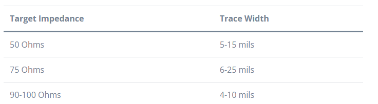
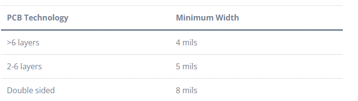
The PCB Trace Spacing Regulation Standards.
Various industry groups and standards agencies determine the regulations governing PCB trace spacing. These standards make sure that, to avoid signal interference, electrical leakage, and other problems, the distance between traces on a printed circuit board (PCB) satisfies specific specifications. The following significant factors determine how far apart traces are spaced on a printed circuit board (PCB):
Rules for Trace Spacing Design
The following design guidelines are commonly applied when determining PCB trace spacing:
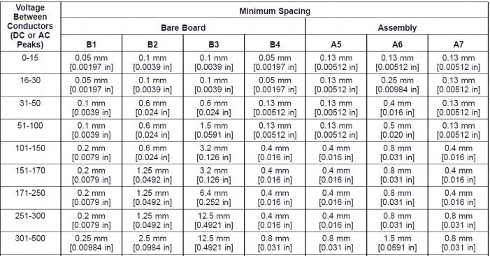
Considering Voltage
Greater distances between higher voltage traces are necessary to avoid arcing. Standard design guidelines:
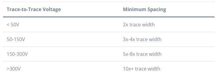
Considering Impedance
A wider distance increases impedance by lowering capacitive coupling. As an illustration:
Predicted on the Prevention of Crosstalk
Noise coupling is reduced by greater distances between high-speed digital or analog traces:
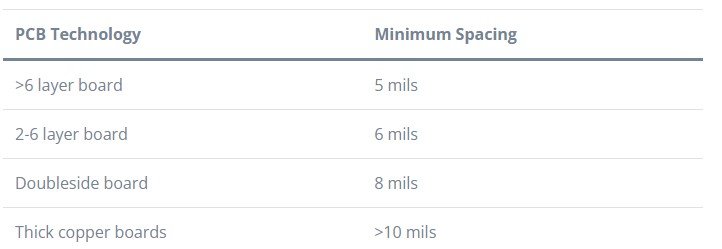
Manufacturability-based Respect tolerances and capacities of the fabrication process:
Margin of Safety
Margin addition shields shorts from process unpredictability:
10–20% additional margin space
Greater leeway in prototype compared to production Reliable trace isolation is ensured through the careful use of suitable design criteria.
Rules for Trace Width Design
Trace width selection is guided by similar considerations:
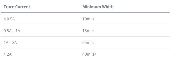
Higher current handling is possible with thinner traces based on current:
Based on thermal rise restrictions, additional widening might be required. Considering Impedance Greater impedance results from narrower traces:
Manufacturability-based Compare the trace width to the manufacturing capacity:
PCB Design Guidelines:
Reducing Interference
It is PCBs’ worst enemy. Don’t worry; we’ll provide you with design principles to lessen this threat. Adopt these strategies to produce high-performing, crosstalk-free devices.
Boost the distance between traces.
More space between traces prevents inductive and capacitive coupling. Give your traces some breathing room, and the chatter will decrease.
Make use of ground planes
Capacitive coupling is decreased by separating signal traces with a ground plane. It also minimizes inductive coupling by giving currents a return path. Your allies are the ground aircraft. Make use of differential signaling. Send complimentary signals at the same time. Signal integrity is improved via the cancellation of noise and interference.
Apply impedance control.
Match the impedance of traces to eliminate reflections and distortions. Crucial for high-speed designs, impedance control maintains signal quality.
Shield your traces.
Guard traces, copper planes, and shielding materials protect against interference. Safeguard your traces, and let them thrive.
Optimize trace routing.
Route traces at right angles and stagger them on different layers. Utilize vias for transitions between layers.
Mind the trace length.
Keep trace lengths as short as possible. Less length equals less chance for crosstalk.
Consider trace width.
Wider traces reduce inductive coupling. Experiment with trace widths to find the ideal balance.
Think about Board Edge Clearance
Another factor to consider during panel construction is board edge clearance. It prevents harm by acting as a shield for the copper and board components.
Design for Manufacturability: Optimizing Depanelization
Release in Tabs for Breakouts
There are two methods for depanelizing PCBs: breakout tabs, which create tiny tabs in between the PCB designs. There is a gap on the panel between these tabs. There should be 0.125 inches of space between the copper and the components and the tab.
Clearance in V-grooves
Cutting the V-grooves, which are pre-scored V-shaped marks positioned beside the board edges, is an additional technique for depanelization. The components in V-grooves should have a 0.05-inch clearance, and the copper should have 0.02 inches of clearance. A delicate art, efficient PCB routing strikes a balance between electrical needs and physical limitations. Understanding the function of routing and how to get the best outcomes requires knowing this. Routing, or “tracking,” the board involves skill and accuracy, from using an auto-router carefully to making sure high-speed signal routing is applied appropriately.
Employ Auto-Router Moderation
Even though auto-routers can greatly expedite the routing process, it’s not always a good idea to rely just on them. Even though they are automated, auto-routers may not always consider the minute details of certain board designs. It is a tool that should be used in addition to human adjustments, not in instead of them. When used sparingly in conjunction with human supervision, auto-routers can improve routing efficiency and avert certain problems at the design stage that could later need PCB troubleshooting.
Employ High-Speed Signaling
Higher signal speeds are required by modern electronics, which makes high-speed signal routing essential. This method guarantees the least amount of distortion or interference during signal transmission. High-speed signal design in electronic circuits requires even trace widths, careful attention to impedance, and sufficient space between traces. By using such meticulous measures, signal integrity problems are avoided during the routing board nets process, and the device operates at peak efficiency.
Expand the Traces You Draw
Making your traces as wide as feasible is one of the fundamental principles of PCB design. In addition to improving performance and lowering the possibility of overheating traces, wider traces can carry higher currents and provide lower resistance. Additionally, they are less prone to manufacturing problems, which results in fewer errors and disruptions during PCB CNC routing procedures. The fact that larger traces can withstand greater power levels without suffering appreciable energy loss is another important benefit.
Put Daisy Chain Routing Into Practice
Using a technique called Daisy Chain Routing, parts are linked together in a succession, akin to a chain’s links. When routing buses with several similar components, like RAM chips on a memory module, this technique is quite helpful. The signals are routed through each component in turn rather than going straight from one to the main source or other component. This produces a layout that is more ordered and uncluttered, which is advantageous for boards that have limited space. Particularly in high-speed designs, the signal delay that is added as it moves through each component in the chain must be taken into consideration. The ability to require fewer layers on a network is another benefit of daisy chain routing.
Employ Stack Multilayering
There is a pressing need to reduce size while retaining functionality in the rapidly evolving field of electronics. This goal is satisfied by the Multilayer Stackup Design method. As the name implies, this method routes more traces in the constrained board area by using many layers of the PCB. Because interior layers can operate as a shield against external noise sources, this promotes superior electromagnetic interference (EMI) shielding and allows for a more compact design. Separate layers for power, ground, and signals can also greatly enhance the performance of the PCB by lowering crosstalk and enhancing impedance management.
Use the Buried and Blind Vias
In PCB design, vias are crucial because they enable connections between various layers. Conventional through-hole vias pass through the whole board, but they might take up valuable routing space in high-density systems. Go into Buried and Blind Vias. Blind vias do not go over the whole board; instead, they connect one or more inner layers to an outer layer. Buried vias are entirely contained within the board and connect two or more inner layers. These tailored vias can significantly reduce potential interference locations and improve signal integrity, all while saving a substantial amount of space. However, using them makes the production process more complicated. Thus, even if they have obvious benefits, it’s important to balance them against the additional expenses and production difficulties.
Techniques for PCB Thermal Management
You might want to be aware of the best PCB thermal management strategies to avoid excessive heat because it can lower the performance of your PCB. For better heat dissipation, a lot of PCB designers use cooling fans, thermal via arrays, and heat sinks. In their thermal design of PCBs, they might also incorporate heat pipes and thick copper traces. Consider the following methods for heat dissipation as you strive to optimize your PCB for thermal management: Warmth Sinks
Metallic vias intended to conduct heat in a PCB are referred to as heat sinks. These metallic vias transport heat from the top layers to the insulating layers, distributing it across the PCB. Heat dissipation is possible because of this technique, which transfers heat to a copper plane. Engineers typically mount heat sinks to parts that produce heat, such as power transistors and switching devices. You should anticipate that these devices will disperse heat across wide areas and transfer heat to the surrounding environment.
Heating Pipes
Heat pipes are a wonderful option for thermal management on a PCB with limited space. Because they aid in passive heat transfer, they are frequently utilized to support tiny electronics. To absorb heat, these pipes include trace amounts of water, acetone, nitrogen, and ammonia. Heat-absorbing fluids condense into vapor, which is then sent through a pipe and into a condenser. The vapor is subsequently condensed by this condenser, returning it to a liquid state.
The heat pipe can then resume the cycle by utilizing the fluid to absorb heat once more once the vapor condenses back into a liquid. Because these pipes have no moving components and can operate quietly and vibration-free, several industries employ them in PCBs. They also don’t need a lot of care and are excellent thermal conductors. Fans for cooling
Using cooling fans increases PCB thermal resistance in another way. Heat buildup can be avoided by installing a cooling fan to a PCB, which allows hot air to be forced out of the area. Cooling fans help remove heat more thoroughly and quickly, which is why high current power supplies usually utilize them.
Via Arrays for Heat
Using thermal via arrays is one of the primary PCB thermal approaches. These thermal via arrays support the PCB’s appropriate heat conduction. Since proximity allows these devices to dissipate heat more quickly and effectively, they function best when placed close to heat sources. Simple vias and filled and capped vias are the two primary forms of thermal via arrays that are typically seen in PCBs. Since they greatly lower the PCB’s thermal resistance, simple vias are frequently a preferred option.
However, because PCB designers can position filled and capped vias beneath a thermal solder pad, they typically offer better performance. They may draw heat straight from the source thanks to their positioning. However, because PCB designers can position filled and capped vias beneath a thermal solder pad, they typically offer better performance. They may draw heat straight from the source thanks to their positioning. Because of its copper filling, which stops uncontrollably large solder flow and cavities from forming in the via during reflow soldering, a filled and capped via also performs very well at dissipating heat.
Heavy Copper Wires
A PCB’s ability to dissipate heat can be enhanced by thick copper traces because additional copper permits heat to disperse over a greater surface area. Thick copper traces are typically used by businesses for high-power applications. Additionally, thick traces will be used to help cool components with significant thermal dissipation.
Essentials of PCB Routing for the Contemporary Designer:
Differential Pair Routing
When a plane ground offers a return path for the signal to flow, that is known as single-ended routing. Single-ended routing has a few drawbacks, including low signal-to-noise ratio, crosstalk, and electromagnetic interference. The most exciting aspect of differential pair routing is that interference will exist equally in both signals so that the receiver can cancel out the signal, even though differential routing requires two signals with opposite polarity but the same magnitude to transfer a single data signal from another.
You must pay attention to trace width, spacing, and other performance factors to guarantee the best possible performance from differential pair routing.
Routing Complex ICs
You must comprehend the fundamental configuration to comprehend the setup and regulations of routing sophisticated ICs. To accomplish the desired downsizing, compact routing is squeezed into numerous layers to create reduced trace widths for sophisticated integrated circuits. Complex integrated circuit routing is a high-speed constraint that needs a predetermined schematic. In this case, you must make sure that the entire ground path stays extremely close to the receiver that provides you with the least amount of data.
Making Use of AutoRoute
Using automated PCB routing ensures optimal resource utilization with accurate time management. Tracing routing manually gets very difficult when working on a larger board. You can complete the task faster with the auto router’s assistance. Numerous CAD systems and PCB design tools with auto router features are available; they are rather simple to use and produce excellent results.
If you are persuaded to get an auto-router, you must comprehend and become familiar with the crucial guidelines and limitations that determine net classes based on the trace widths and spacing of each board. A thorough comprehension of the regulations might help one realize the intended design. Running traces across the component placement and routing must be avoided. Before analyzing the configuration, perform a route cleanup to check the routing of the circuit.
Additional PCB routing approaches and advice
Different PCB routing suggestions apply to analog parts, terminal components, connectors, and other components. Look at these pointers:
To find out the exact width and spacing needed, speak with the PCB maker.
To guarantee a steady current flow, you will want power and broader ground connections.
The ground and power must be kept close to one another to minimize inductance and prevent noise in the circuit.
Depending on the circuit, different trace widths will be present in the power supplies.
Large spacing is required when working with high-speed traces to avoid any type of crosstalk.
It can be concluded that having sophisticated routing tools and approaches can greatly enhance designs With the correct guidelines and resources, you can complete even the most challenging designs. Both manual and automatic methods have their merits, but to stay current and produce well-designed PCB designs that meet your needs, you should keep up with the newest technological advancements.
Prospective Developments in PCB Panelization
Miniaturization Difficulties and Solutions
Miniaturization creates new difficulties for PCB panelization as electronic devices get smaller and smaller. To ensure that depanelization techniques can support complex layouts while preserving quality and dependability, designers and manufacturers will need to work closely together. Sophisticated materials and fabrication methods will be crucial in overcoming these obstacles.
Keeping Up Quality and Dependability
Techniques for Testing and Inspecting
Assurance of quality is still the top priority in PCB depanelization. Strict testing and inspection protocols are necessary to find flaws, such as bad components or solder joints, before they become more serious difficulties. Techniques like X-ray testing and automated optical inspection (AOI) are frequently employed to guarantee the integrity of depanelized PCBs.
Reducing the Risks of Panelization
Panelization has several advantages, but it also has certain inherent dangers, like the possibility of uneven solder paste distribution or stress concentration at V-cut lines. Designers and manufacturers need to be very deliberate in their planning and validation to reduce these risks. Minimizing potential problems also involves selecting the right materials and following industry guidelines.
Aspects of Sustainability and the Environment
Cutting Down on Waste in Depanelization One important component of sustainability is less material waste, which is achieved by efficient penalization. Through the optimization of panel layouts and the reduction of inter-PCB space, manufacturers can effectively minimize the quantity of scrap material produced during the manufacturing process. This environmentally friendly strategy fits nicely with the increased focus on sustainable production methods.
Eco-Friendly Practices and Materials
Further improving sustainability can be achieved by depanelization that uses eco-friendly materials and procedures. For example, using lead-free solder complies with standards and lessens its impact on the environment. When creating panelized PCBs, designers can also investigate the usage of recyclable materials and take end-of-life disposal options into account.
Conclusion
To correctly implement a circuit design on a working PCB, well-thought-out routing techniques utilizing both automation and manual tweaking are necessary. Both novice and seasoned designers will benefit from using the techniques in this guide to create routing layouts that are clear, effective, error-free and ready for manufacturing. It is time well spent to pay attention to routing to prevent hassles caused by a board layout that is not ideal. Proper PCB layout guarantees correct signal transfer and improves circuit response as devices get smaller and more sophisticated. It preserves dependability, minimizes interference, and protects signal integrity. Noise, unreliability, and signal distortion can result from poor routing. Thus, it becomes crucial to become proficient in PCB routing. Expertise is needed to navigate obstacles like high-speed signals and intricate architecture. It is essential to maintain controlled impedance, appropriate location, and strict adherence to design limitations. These subtleties are enhanced by multi-layer PCBs, which permit increased component density, enhanced signal isolation, and effective power distribution.
PCB Runner offers custom design layout services for all industries and critical design requirements. Our expert design layout team efforts help the end R&D / product engineers to reduce their time by being back & forth to design PCB based on manufacturing capabilities & running DFM & DFA twice. Please submit your schematics & BOM files to our email at sales@pcbrunner.com or engineering@pcbrunner.com for quick design layout estimations.
Exploring PCB Solder Masks: Types, Colors, and Future Trends
Introduction:
Printed circuit boards (PCBs) are coated with a polymer layer known as solder mask (sometimes called solder resist) to control solder spreading and avoid solder bridges during assembly. Additionally, it aids in shielding traces from electrical leaks and environmental deterioration. To assist PCB designers in making the most effective use of this crucial material, this page discusses solder mask types, qualities, functions, design concerns, application techniques, and faults.
Applied permanently on the surface of finished PCBs, solder mask—also referred to as solder resist, solder stop, or solderable mask—is a thin layer of insulating material similar to lacquer. The solder mask’s primary purposes are as follows:
Preventing environmental corrosion and oxidation of exposed copper
Preventing the formation of solder bridges during assembly between pads that are closely spaced.
Live nets that are electrically insulated to avoid shorting.
Enabling the selective plating or coating of exposed portions
Most completed circuit boards have a green solder mask covering most of the surface, leaving exposed metalized pads and traces for soldering. It adds a unique look to manufacturing boards in addition to silkscreen.
However, solder masks have uses far beyond aesthetics. Correct design and use significantly improves the manufacturability and reliability of PCBs.
Four Primary PCB Solder Mask Types
Solder mask, sometimes referred to as solder resist, is a robust, long-lasting coating that shields printed circuit boards’ (PCBs) copper traces and their interfaces. A solder mask’s primary purpose is to stop conductive solder from bridging between various electrical components and creating short circuits. There are numerous varieties of PCB solder masks, including top- and bottom-side masks, epoxy liquid, liquid photo imageable, and dry film photo imageable.
Masks on the Top and Bottom
The electronic engineer can see the holes in the green solder mask layer that was applied to the PCB using film, epoxy, or ink processes by using a topside solder mask. Using those marked locations, component pins can subsequently be soldered onto the board. Top traces refer to the conductive trace pattern on the top side of the circuit board, whereas bottom-side mask designates openings on the lower surface.
Liquid Epoxy
The least expensive kind of solder mask is epoxy liquid, which is silkscreened onto the PCB layout. The thermosetting polymer epoxy has a wide range of uses. A woven mesh is used in the printing process known as “silk screening” to support stencils or patterns intended to obstruct ink.
Ink can transfer to open spaces created by the mesh. While silk is frequently employed in art, synthetic fibers are more frequently used in electronic applications. Thermal curing is the last step in the finishing process.
Fluid Ink Capable of Photo image
The liquid photo imageable solder mask is supplied in the form of an ink. The PCB can be coated with ink by spraying or silk screening it, exposing it to the design, and then developing it. Hot air surface leveling is one kind of procedure that is frequently employed with liquid ink formulations (HASL). It needs a spotless setting devoid of impurities and particles. Following the UV light exposure phase, developers—high-pressure water sprays—are used to remove the mask. Thermal curing and organic coating are necessary for circuit board finishing.
Photo imageable Dry Film
Vacuum lamination is used to apply a dry film photo imageable solder mask, which is subsequently exposed and developed. Parts can be soldered to the copper pads once the pattern has been established after development. Electrochemical processing is used to layer copper onto the board inside the holes and on the trace sections. The copper circuitry is shielded with tin. After that, the exposed copper is etched and the dried film is removed. Thermal curing is another step in finishing.
Factors influencing the solder mask color selection
Visibility and contrast
Enhancing the contrast and visibility of your PCB marks and components is a primary motivation for selecting a solder mask color. If you use a magnifying glass or a microscope, a high contrast color can assist you locate and examine the vias, silkscreen labels, and solder connections on your PCB. Although a low contrast color can conceal certain flaws or errors, it can also give the impression that your PCB is more consistent and smooth. In general, colors that are high contrast include green, blue, and red, while colors that are low contrast include black, white, and yellow.
Both branding and aesthetics
Enhancing the aesthetics and branding of your PCB design is another justification for selecting a solder mask color. The color of your solder mask might express your brand, your organization, or the theme of your product. For instance, you may want to pick a color that is bold or distinctive to set your PCB apart from the crowd, or a color that is subdued or neutral to go in with the surroundings. It could be a good idea to coordinate the color of your solder mask with the enclosure, your logo, or other design components. But you should also think about how the color of your solder mask influences your PCB’s durability, solderability, and heat dissipation.
Guidelines and policies
Adhering to the rules and specifications that are relevant to your PCB design is the third justification for selecting a solder mask color. Certain industries or applications, like the military, medical, or automotive sectors, could have particular demands or suggestions about the solder mask color of their printed circuit boards. For instance, some medical PCBs use white solder mask to denote cleanliness and sanitation, whereas some military PCBs use red solder mask to show excellent reliability. Before selecting the color of your solder mask, you should always make sure it complies with all applicable rules and laws. These can have an impact on the functionality, security, and caliber of your PCB.
Price and accessibility
Taking the price and accessibility of your PCB fabrication into account is a last justification for selecting a solder mask color. Depending on market supply and demand, different solder mask colors may have varying costs and lead times. Since most PCB manufacturers utilize and supply green solder masks, it is typically the most affordable and common hue. Certain colors could need unique materials or methods, which could make them more costly or take longer to produce. Before selecting the color of your solder mask, you should always check with your PCB manufacturer as they can have different possibilities and restrictions.
Advantages of covering bare copper on a PCB with a solder mask
Using a solder mask over bare copper on a PCB has numerous advantages. Among its primary advantages is its potential to shield copper from oxidation. Also, it may aid in preventing solder from bridging copper lines next to one another. By creating a barrier between the copper and the environment, a solder mask can shield the metal from oxidation and other forms of deterioration.
Furthermore, a solder mask can act as a sort of barrier between the PCB’s various conducting layers. By doing this, crosstalk can be decreased, and the PCB’s overall electrical performance can be enhanced. By creating a low-impedance channel between the copper traces, this can enhance the PCB’s electrical performance.
Design Considerations for PCB Solder masks
Solder mask is a crucial component in assuring the correct operation and dependability of the finished product, and PCB design encompasses many other important considerations. It’s important to take a number of factors into account while designing a PCB using solder mask, including material choice, thickness, tolerances, and clearance needs. We’ll talk about these design factors in this part and offer tips to help you make the best PCB design possible for a solder mask application.
Selection of Materials
Solder mask materials come in a variety of forms, as was previously mentioned, and each has special qualities and functions. Think about things like electrical insulation, flexibility, chemical resistance, and thermal stability when choosing a solder mask material for your PCB design. To select the best material, consider the needs and operation environment of your PCB. To find out which solder mask materials are suitable for your particular design, speak with your PCB maker.
Thickness of Solder mask
The PCB’s overall performance, including mechanical stability, electrical insulation, and thermal management, can be impacted by the solder mask layer’s thickness. You must weigh these considerations and make sure that your design complies with industry requirements in order to decide on the right thickness. For suggestions on solder mask thickness, refer to the IPC guidelines. To find out the maximum solder mask thickness that will work for your design and production process, speak with your PCB manufacturer.
Registration and Tolerances
For the solder mask layer to be precisely aligned with the copper traces and pads underneath, solder mask tolerances and registration are essential. To prevent solder bridging or shorts during assembly and to shield delicate components from the elements, alignment must be done correctly. Utilize the solder mask design guidelines and tolerances that are acceptable for the capabilities of your PCB manufacturer. Incorporate alignment features or fiducial markers into your PCB design to enable precise solder mask registration during production.
Clearances & Openings at solder mask
The regions of the PCB where the solder mask is purposefully left off to facilitate soldering, testing, or other activities are known as solder mask clearances and apertures. For PCB assembly and functioning to be successful, these areas must be defined correctly. Based on component pad sizes, soldering specifications, and manufacturing tolerances, design solder mask clearances. If more space is required, add it for test points, fiducial marks, or other functional requirements.
You may maximize the performance, dependability, and manufacturability of your PCB design by giving careful thought to these solder mask design considerations.
What color of solder mask should be? The dye that is utilized in the solder mask material determines the color of your solder mask, and the cured solder mask thickness is influenced by the chemical properties of the dye. The ability to produce thin solder mask dams (~0.1 mm) is one of the reasons green solder stop mask is so widely employed. Different colored solder mask dyes typically result in thicker solder mask dams. IPC-SM-840D defines solder resist thickness on PCBs for usage in specific industries or applications, regardless of the dye you choose to employ.
A crucial component of automated or human visual inspection is the color of the solder stop mask. The least contrast between the board and traces is produced by black solder mask, which can make automated inspection challenging. This is an additional justification for favoring green masks. During manual inspection, the color of the silkscreen you choose will also affect visual contrast and visual fatigue.
You should prepare your design to account for the sensitivity of your final application, just like you would with any other fabrication parameter or process. It’s crucial to talk to your manufacturer about your fabrication possibilities at all times. Depending on their ability, they might even be able to recommend better choices.
Which Solder Mask Is Best ?
The physical dimensions of your board, the holes, components, and conductors, the surface layout, and the intended use of your product all play a role in selecting the right solder mask. You will need a photo imageable solder resist for the majority of contemporary printed board designs. A liquid or dry application will depend on the topography of the surface. A dry application applies a consistent layer of solder mask to the whole surface. Nonetheless, a particularly flat board surface is ideal for dry mask adhesion. For improved contact between the copper of your traces and the laminate, you’re usually better off using a liquid (LPSM) option if your surface characteristics are intricate. A liquid application’s drawback is that the thickness isn’t consistently the same.
Additionally, you can apply various finishes to the mask layer. Discuss what your manufacturer has available and how it will impact production with them. For instance, if you are employing a solder reflow process, a matte coating helps to minimize solder balls.
Solder masks are required for PCBs produced by the solder reflow process. The quality of the reflow might be impacted by the mask’s polish.
The range of colors for Solder Masks in printed circuit boards: advantages and disadvantages
Green
For good reason, green solder masking is currently the most widely available hue on the market. It is a suitable hue for maintenance and repairs because it provides one of the biggest visual contrasts of any accessible color between planes, traces, and empty areas. Owing to its widespread appeal, almost all large-scale PCB manufacturing facilities can obtain it, and it is regarded as the standard hue for circuit boards globally. It is also the least costly circuit board color that is offered as a result. It has one of the thinnest coats and can hold the smallest solder mask dams to avoid solder bridging because of intensive research and development.
Red
A visually arresting choice, red solder masking is frequently utilized in designs that highlight interior hardware. The hue is now among the most often used alternate PCB colors, but there’s a catch: it’s less visible and has less contrast than a typical green PCB. When doing maintenance on a red PCB, technicians might need to use more magnification to see problems on the board. Almost always, people choose red for its beauty rather than its usefulness.
Blue
Though it has less contrast than circuit boards that are red, green, or yellow, blue is the second most popular hue utilized in the production of PCB boards. They are usually connected with open-source electronic projects since they are the preferred color for Arduino boards due to the way silkscreen appears on them. Furthermore, the coloration of blue solder masking makes it perfect for installation behind LCD screens.
Black Compared to other colors, black solder masking is one of the priciest color options and frequently requires more time to make. It should not be used in high-heat applications because of its propensity to absorb heat. It also has very little contrast, which makes maintenance and repairs challenging. Additionally, during the production process, it has the highest failure rate.
Silkscreen looks really good on black PCBs, despite the low trace contrast on these boards. It is also the least reflective light, which makes it perfect for circuits where light is undesirable. While black solder masking may be visually appealing to businesses such as Apple that value sophisticated design, it is seen as a challenging hue to work with from a practical standpoint. Selecting a circuit board with a black print should be done carefully.
White
White PCBs are the hardest to visually analyze since they have even less contrast than black PCBs. Over time, they also clearly gather dirt. White solder masking is frequently used with LED lights, especially when they are attached to surfaces with lighter colors. When the lights are on, white offers the least noticeable color and blends in the best. Since white is one of the colors that reflects light the most, it also emits pure white light when lit. Make sure your manufacturer is utilizing a solder with high reflectivity when choosing white PCBs for LED applications, as not all solders are created equal.
Future Trends in Solder Mask Technologies
There is a constant exploration for new developments in materials and methods to deliver the highest quality product possible as technology continues to advance toward tighter features and larger circuit densities. In terms of capital expenditure and collaborating with suppliers to overcome these issues related to material, process, and quality, Advanced Circuits is still in the forefront. Our investment in enhanced solder mask (SM) materials and laser direct imaging (LDI) equipment will give the best overall quality solution to fulfill current and future technological demands. Advanced Circuits Colorado will start switching to the higher performance solder mask on October 23 in order to specify the tight SM features that are frequently encountered in modern technology. This solder mask is intended for LDI.
Thermal management
More thermal management will be a top priority for solder masks in the future. This is to account for the increasing power density of contemporary electronics. Maintaining optimal performance will require improved heat dissipation qualities.
Nanotechnology
In the formulation of solder masks of the future, nanotechnology may be extremely important. Better feature resolutions and general performance enhancements might be made possible by it. Precision and miniaturization could advance as a result of this integration.
Customization
More customizable solder masks are probably in store for the future. This is a result of the growing popularity of flexible and wearable electronics. This will enable stretching and bending without compromising functionality. This evolution aligns with the growing demand for flexible printed circuit boards. They are employed in numerous contexts.
Conclusion
In order to safeguard the copper traces on PCBs, solder masks are necessary. It offers defense against short circuits and oxidation. Manufacturers must to be knowledgeable about the appropriate thicknesses and methods for integrating the electronic components on PCBs. They ought to adhere to industry norms as well. Because it acts as an insulator between conductive traces, resists corrosion, and stops solder bridging, the solder mask is a crucial component of a printed circuit board. Bare copper is frequently used as traces by PCB fabrication businesses, yet it is quickly oxidized, corroded, and destroyed. When exposed to aqueous solutions, such as water, bare copper traces will oxidize as well. Make sure a solder mask covers the copper in order to solder to bare copper effectively. If not, the copper will not be soldered to the solder. Additionally, flux should be used if you’re not soldering to bare copper and you’re not using a solder mask.
PCB Runner offers a variety of solder masks colors including LDI & LPI methods. Do reach out to our team for custom requirements quote, you can submit your Gerber files on https://www.pcbrunner.com/free-pcb-quote/ or do reach out to our team offline at engineering@pcbrunner.comor sales@pcbrunner.comfor your current or upcoming projects needs.
Exploring PCB Via Types: Choosing the Right Vias for Your Design Needs
Introduction
Vias are holes that allow conductivity to go through the board’s layers in printed circuit boards. Every hole serves as a conductive channel for the transfer of electrical signals between circuit layers. A printed circuit board has levels that vias go through. Depending on how the PCB is designed, the board may need a hole that passes through each layer from top to bottom. On the other hand, some vias go through an inner layer, while others only reach the top or bottom layer. Vias on a printed circuit board come in a variety of options. One of the most important components of a printed circuit board is the via. As a result, they bear a substantial portion of the expenses associated with the production of boards.
Even though all of these via types have the same basic function, some PCB designs will fit one via type over another more than others. This article discusses the many via types used in printed circuit board design and how they can be used to help with electrical connections.
PCB Via Types
On a PCB, there is a via that connects at least two layers, allowing power or signals to move between them. A copper-plated cylindrical barrel that serves as a conductive channel is present in every PCB via. In PCBs, a variety of via types are used:
Through-hole These vias can connect to any layer and are available throughout the PCB stackup. Every layer of these PCB vias will feature a pad where a connection to a trace is made.
Blind vias These end at a landing pad and extend from an outside layer to an interior layer. Signals can then pass via an internal layer by connecting the pad to another trace.
Buried vias
These do not reach the surface layers; instead, they extend between two interior layers. Like regular vias, buried vias can connect on any layer between their starting and terminating layers.
Microvias They are basically miniature blind or buried vias that span one layer at most, or two layers at most in cases of extremely thin dielectric (the latter being referred to as a skip via or skipped microvia). stacked microvias. Vertical stacks of blind and buried microvias, or stacks of several buried microvias, spanning multiple levels are known as stacked microvias.
Via -in-Pad Using vias on ball grid array (BGA) pads—also referred to as via-in-pads—is one of the more widely used printed circuit board designs of today. The vias of the via-in-pad design are positioned on the PCB’s BGA pads. Because the design allows manufacturers to reduce the amount of space needed for vias, it has gained popularity. Because of this, via-in-pad enables producers to create printed circuit boards that are thinner and require less room for signal routing. For today’s small electronic and computing devices, which manufacturers have made to fit inside pockets and occasionally around wrists, via-in-pad technology is ideal.
When to Use Each Type of Via: Matching Application to Functionality
Through-hole: This is the type of via that is used most often in a circuit board. The holes are drilled all the way through the board with a mechanical drill bit and can get down to 6 mils in size.
Buried via: This via only connects internal layers of the board and is useful for PCBs with very dense routing. Blind via: This via starts on either the top or bottom of the board but doesn’t go all the way through it.
Microvia: For hole sizes smaller than 6 mils, a laser-drilled microvia is used. These vias connect only two adjacent layers of the board and can be on the surface or buried within the board layer stack up. Microvias are extremely versatile and can be stacked together, or on top of a buried via, but have a higher fabrication cost associated with them.
Via-in-pad (VIP): These vias can either be standard thru-hole vias or microvias, but their position in a surface mount pad makes them unique. If a standard mechanical drill is used, the via will require extra fabrication steps to prevent solder on the pad from flowing down through the hole. Microvias on the other hand don’t have this problem, but they can be more difficult to fabricate due to the tighter trace and space tolerances in a high-density design. A path that sends a signal from a source to a receiver is called a via. Effects of inductance on via design and low capacitance on signal integrity have been demonstrated. It will be demonstrated that this return path may be regulated with careful via environment design, allowing vias to be sorted out according to cable specifications within specific frequency ranges. This indicates that the via stubs effect is addressed, as are ways to lessen it by moving undesired resources outside of the area of interest. This indicates that the via impedance can be adjusted to meet a certain goal in order to reduce reflections.
How to Choose Via’s for a PCB:
Taking Design into Account Assess the requirements of your PCBA project first. Evaluate factors including signal quality, heat control, power distribution, and required space. Controlled impedance vias may be required for high-speed signal traces in order to preserve signal integrity, and suitable ground and power via arrangement is essential for the best possible power distribution and heat dissipation.
Via Size: A device’s heat dissipation efficiency and current carrying capacity are determined by its size. Better heat dissipation and less resistance are provided by a bigger via. A densely packed PCB is better served by a smaller via. The precise design specifications determine how to strike a balance between utility and size.
Plating: To guarantee electrical conductivity, vias are frequently plated with copper. Plating influences dependability and performance. To improve corrosion resistance, pick between through-hole copper plating and other methods like ENIG.
Aspect Ratio: The ratio of diameter to via depth is known as the aspect ratio, and it is important. Drilling difficulties, uneven plating, and decreased dependability might result from a high aspect ratio. When choosing the aspect ratio, consider the production capacity of the PCB manufacturer of your choice.
Via and Layer Count: Selection is influenced by the PCB board’s layer count. Blind and buried vias are frequently used in multilayer boards to maximize signal quality and space utilization. But producing these vias is difficult and can get expensive.
Testing and Simulation: Analyze the effects of various vias on overall functionality, signal quality, and thermal performance by using simulation tools. Before any manufacturing happens, problems are found and the design is optimized through virtual testing.
Thermal Considerations and Heat Dissipation with VIAs
PCB Using channels (through-holes) that pierce through the PCB, heat dissipation holes, also known as PCB thermal vias, are a technique used to dissipate heat to the backside of a PCB. They are positioned as close to or directly beneath the heat-producing element as feasible.
By employing the PCB as a heat sink, heat dissipation holes help surface-mounted components dissipate heat more effectively. They entail drilling through holes in the PCB structurally. Connecting the copper foil on both sides of the PCB increases the surface and volume accessible for heat dissipation, which lowers thermal resistance in single-layer and double-sided PCBs.
The similar goal can be accomplished for multi-layer PCBs by joining the planes between layers or restraining connections to particular layers.
Thermal Via Design
In multi-layer boards, vias offer low heat resistance conduction channels between layers:
Quantity Increased via number minimizes lateral spreading before heat enters a via by reducing conduction channel lengths in the in-plane direction. But costs go up with additional vias.
Arrangement Scheme In comparison to peripheral distribution, gridded arrays provide superior heat dispersal from hot regions. It’s also possible to see mixed patterns.
Density and Size Although they take up more routing area, wider via diameters and higher via densities enhance vertical heat conduction. Laser micro-vias contribute to higher density.
Depth Compared to partial depth vias, full depth vias that span the entire board thickness transport heat to inner layers more effectively.
Barrel Plating Depth Via barrels with thicker plating have less conduction loss via the via. A higher current rating is also permitted.
Size of Anti-pad Better heat dispersal into plane layers is achieved with larger anti-pads or clearing spaces surrounding vias. However, it also shrinks the signal layers’ routing space.
Pads for Thermal Relief Heat from plated through-hole vias is kept out of the solder mask by exposed thermal pads. Temperatures are lowered by the enhanced heat transmission.
Stuffing Heat is transferred to interior layers more quickly in filled vias with conductive inserts than in hollow vias that solely rely on barrel plating.
Manufacturing Constraints and Cost Implications
Production Constraints: It is important to consider the capabilities and constraints of the production process. Requirements for things like annular ring width, aspect ratio, minimum drill size, and pad size should match the capabilities of PCB production and assembly procedures. Respecting these limitations guarantees manufacturability and keeps possible production-related problems at bay.
Cost and Reliability: Aspects of cost and reliability should be taken into account when optimizing the route design. While too many vias could raise production costs, improper via location or size could affect the PCB’s dependability and functionality. Achieving a dependable and affordable design requires striking a balance between these variables.
Advanced Via Frameworks and Methodologies
With recent developments in via fabrication, PCBs can be made denser and more complicated, enabling increased capabilities. Here are some cutting-edge technologies and via types:
Back drilled Vias: The stub portion of the via is removed by mechanically drilling off the via barrel after it has extended through the pad on the outer layers. This lowers stub resonance for high-speed signals considerably.
Filled & Capped Vias:
Compared to just plated vias, completely filling a via’s hole reduces the possibility of contamination and increases heat transfer. Capped vias have protective epoxy covering only the end holes.
Tented Vias: To completely isolate tented vias and keep solder and debris out of vias not used for component terminals, a layer of solder mask coating is applied.
Via in Pad (VIP): By positioning drill pads over function pad centers, VIP enables vias to be implanted straight into footprints, preventing routing channels from being blocked.
Microvias Assisted by Lasers: Lasers create tiny holes that are impossible to drill with mechanical tools, allowing for direct copper plating without the need for seeding.
PCB Vias Design Guidelines for Buried, Blind, and Through-Hole Vias
Every one of the aforementioned PCB kinds has unique design guidelines. The same is covered in this section.
Hole-through PCB Vias
Every layer of the circuit board needs to have a drill pad for through-hole PCB vias. While it should be small, the drill pad should be big enough for the drill being used.
Additionally, in order to prevent short circuits between adjacent holes, the through -hole via requires a conventional anti-pad on the board’s plane layers.
Choosing the right via size is a crucial design guideline for through-hole PCB vias.
The aspect ratio of the drilled hole in relation to the thickness of the board should be considered while selecting the via sizes.
The residual or unused via barrel in the multi-layer circuit board may function as an antenna if a through-hole via can connect high-speed signals between the first two layers. But this could lead to problems with signal integrity. OEMs use back drilling to get around this issue. Nevertheless, the overall cost of fabrication goes up with this procedure. To increase board performance, using blind and buried or micro vias is the ideal approach. If necessary, through-hole vias can be covered or filled. The PCB designer gives the fabricator precise instructions for this.
PCBs buried via
Buried vias, as previously mentioned, link the circuit boards’ inside layers, which are not in contact with the exterior layers. For a single connection, the hole needs to be defined as a distinct drill file.
Buried vias, as previously mentioned, link the circuit boards’ inside layers, which are not in contact with the exterior layers.
For a single connection, the hole needs to be defined as a distinct drill file.
Aspect ratios of at least 1:12 are required.
The maximum distance and overall depth between the corresponding outer layers and inner layers are determined by the small hole.
Mostly helpful for PCBs with thick routing are buried vias.
Blind PCB Vias
Since blind vias are mechanically bored, their drill size restrictions are comparable to those of through-hole drilling. Through in-the-layer stack-up, they permit additional routing channels above or below. Blind vias have a benefit over through-holes because of this capability.
Similar to buried, every hole in a blind route needs to be identified as a distinct drill line.
Aspect ratios ought to be at least 1:1.
The layers of the circuit board are drilled and plated before being fused together in this sort of via, which is constructed sequentially. PCB designers should therefore use them with caution and only when necessary.
How should a micro via for an advanced HDI PCB be designed?
Hole Size: Modify every component of a PCB that has been traditionally intended for microvia design. excessively large holes, or those that will produce a small PCB that is not functional or not ideal.
Copper Thickness: The circuit is connected throughout thanks to patterned plating. Conversely, wire bond plating might be chemical or electrical. Produce robust and stiff FR4 laminates with thin micro double-sided or single circuits for micro via design in order to ensure reliability.
Security Marking: For accurate PCB identification, very tiny individual barcodes can be imaged onto the solder mask.
Future of PCB vias
The PCB industry’s automated assembly technology is a future trend.
SMT Vias
With well-known PCBA manufacturers like JCLPCB and PCB Way embracing this technology, digital intelligence has clearly emerged as a prominent trend in the PCB market. A significant amount of PCBA boards are becoming more and more necessary as market demands change. As a result, Surface Mount Technology has taken the lead and now holds around 70% of the market.
In order to finish PCB assembly, component leads are manually placed into drilled holes on the PCB and soldered to the copper traces on the other side of the board using the conventional Through-Hole Technology. By placing components directly on the PCB surface, the SMT method, on the other hand, avoids the requirement for drilling holes thanks to automated equipment. This comprises a variety of parts, including integrated circuits, resistors, and capacitors.
Build up technology for vias
A common method for creating HDI advanced PCBs is the build-up technique. The inner and outer layers of a multilayer PCB are typically made independently and then pressed together. Additionally, we start with the creation of the inner layers and work our way outward, adding layers on both sides. Laser lasers are typically used to drill blind or buried vias in order to expedite the production process. Furthermore, the build-up technique can result in circuits with finer trace and spacing up to 2 microns. However, plating micro-vias still requires more sophisticated equipment, making it more expensive and challenging.
Via Filling
We may have problems with air bubbles remaining in the laser-drilled blind or buried vias, which impacts the thermal shock resilience of advanced PCBs. The traditional techniques involve using a resin or unique resist to fill the blind or hidden vias. These techniques are not very efficient, though, and they are challenging. Via filling is introduced to fill buried or blind vias by electroplating, which significantly boosts reliability, in order to improve processing. More sophisticated machinery, specialized plating solutions, and the necessary copper weight are required to achieve effective filling, which nevertheless entails difficulty and high expense. PS Electronics is happy to be involved in the development of other cutting-edge PCB technologies, such as Lo PCB, Rigid-flex PCB, and High-frequency PCB.
Conclusion
Vias are required to manufacture multilayer PCBs, which are the way of the future for PCB manufacturing. These PCBs are required to produce the highly functional and compact devices that are the mainstay of modern electronics.
The movement of heat and electrical current between the various layers of a board is facilitated by vias. These vias differ in size and type as well. The kind and dimensions of vias to be used depend on the needs of a circuit board. Vias also improve the signal integrity of circuit boards. Throughout the board, annular rings and multilayer lamination are crucial. Additionally, when creating vias, copper pad and surface components are essential. In PCBs, many vias and signal lines are frequently employed. The outer layers hold significance as well.
PCB Runner handles all type of Via’s categories including blind, buried, stacked & staggered via’s. Do submit your gerber files on https://www.pcbrunner.com/free-pcb-quote/ or do reach out to our team offline at engineering@pcbrunner.comor sales@pcbrunner.comfor your current or upcoming projects needs.
Mastering PCB Design: From Schematic to BOM and Production – A Comprehensive Guide by PCB Runner
A consistent visual depiction of a circuit can be found in a schematic diagram of a circuit board. One of the most important aspects of PCB design is the schematic diagram. A sample circuit board schematic can show how different electronic components are connected. This could be the first action in a device’s strategy. Earlier, circuit charts were drawn by designers on paper. They have started using PCB plan instruments, which simplify the plan preparation process. A well-drawn PCB schematic diagram can significantly reduce the need for later PCB rework.
Creating a Clear and Accurate Schematic
Follow conventional schematic guidelines to create an efficient schematic design.
Page size selection:
The majority of design programs include many page sizes. Depending on how much their circuit plan is estimated, the designer might choose it.
Page naming accord:
The schematic’s logical blocks are divided into pages. Pages are arranged alphabetically by us. Most designers edit the history instead of block charts to save time. When other designers attempt to comprehend the schematic diagrams, they are accommodating. The majority of the organizations participating followed each of these guidelines and customs.
Grid Settings:
The tool needs some reference, but the designers are not immediately required to provide this. Designers can more accurately reference and connect parts when they use a grid. Throughout the examination, circuit components need to be continuously connected to the grid and open to network probing. Page title bar: The page title bar completes all the required information and is situated in the schematic page’s footer. (Page size, modification date, record number, name and purpose of the circuit, and disclaimer from the manufacturer). Remarks: The circuit’s relevant annotations must be written by the designers. Messages can be written on pages of schematic drawings or stand-alone papers. Annotations for intricate patterns are frequently given on different pages. Jumper states and PCB layout limitations and guidelines are a few of the remarks.
Revision history:
Revision history documents alterations made to the layout. The date, a summary of the modifications, the names of the authors and reviewers, and the review comments are all included in the document. Usually, the main or last page of the schematic layout contains the revision history. Directory of schematic documents: This directory contains a list of the subjects covered in the schematic documentation. This website makes it simple for designers to locate particular modules inside a complex design. If the operation is modest and has a straightforward design, you can omit it.
Block diagram:
Block diagrams significantly aid reviewers in understanding the design for a review by speaking to various modules within the plan and flag flow.
Network label agreement:
The schematic is meant to simplify the circuit for designers to understand. The common symbols of an integrated circuit (IC) in PCB design can be reduced when creating a schematic by minimizing the number of unnecessary network connections. Instead of dragging a bunch of networks across the screen, the designer refers to the well-organized title of a specific stick that is connected to a trap on another device. The names of these pins will be the same. The readability of the schematic diagram is increased by assuming that a pin with the same name is connected. When a network is directly connected to another IC on the same page, network naming is not necessary. But you must give it a name if you wish to link the network to an IC on a different page.
Design rules checking:
A clever CAD function called Design Rule Checking (DRC) verifies the logical and physical integrity of a design. The online check can be completed at plan time and is based on all empowered plan rules. Verification of net tables:
Create the netlist as soon as the schematic design is finished and the layout is imported. There are two possible extensions for net table files:mnl and.txt. While the.txt file shows every electrical connection between components, the.mnl files are machine-readable. To prevent design flaws, it is advised that the network be manually verified.
Bill of Materials
BOM generation is currently a crucial capability offered by the CAD tool. If the designer provides all inputs in the tool when building or importing parts from the library, you can generate a complete and sufficient BOM. The manufacturing part number (MPN), package, supplier name, and supplier part number are among the details that can be found on the bill of materials. It is advised to provide all pertinent data while creating symbols.
Beginning with circuit boards, the Bill of Materials, or BOM, is an essential component of any electronic device’s design and manufacturing process. The project might require adjustments in the absence of a comprehensive BOM, which could delay production. As such, one of the most important factors in PCB production is the BOM.
Most of the time, when a customer submits an order, manufacturers request that they upload their BOM list. Nonetheless, it is essential to understand the data that a BOM should contain while designing one. The required information should also be included in the bill of materials. BOMs provide several advantages to consumers and electronic manufacturers alike. Thus, before creating one, it’s critical to comprehend what a bill of materials comprises.
A Bill of Materials: What Is It?
A list of materials, parts, and assemblies needed for product manufacturing is called the bill of materials. Production depends on the data in the bill of materials. Consequently, to produce a product, producers must rely on these bits of information. The BOM needs to be extremely precise and well-detailed. The BOM determines a production’s level of success.
BOMs are essential for producers as well as customers. When a customer orders circuit boards, for example, it is helpful for them to express their needs. To manufacture the circuit board or electronics according to the customer’s requirements, the PCB assembler uses this information. The BIOM can also be used as an ingredient list when producing a product. Creating a BOM is the first step in the production process for all manufacturers. This is so because the product’s basic specifications are provided by the BOM. BOM is utilized by several production sectors in addition to the electronics industry. As the phases progress, the BOM also improves production.
How to make clear and well-organized schematics Space
You must choose how to use the blank space that appears when you first open a new schematic. It relies on several variables, including the project’s size and complexity, target audience, any standards you must adhere to, and the project’s expected life cycle. Additionally, it depends on whether or not you need to print the schematic. Whether you need more than one sheet or if one will do is the most crucial decision to make. Starting with a single A4 page and switching to an A3 sheet as the project progresses is one method for smaller projects.
The Best Component Arrangement for Understanding and Clarity
Logic and Intuition-Based Component Arrangement
To Reduce Signal Crossings and Improve Flow
Making Explicit and Brief Connections Selecting Line Styles and Thickness that are Correct Steer clear of overlapping and unclear connections Assigning Names, Nodes, and Component Labels
Component Labeling:
Every element in the schematic diagram needs to have a label that corresponds to its reference designator. Alphanumeric identifiers known as reference designators are used to identify each component separately. It is important to label the components suitably once the schematic design has been constructed and they are each represented by a symbol. The circuit design is made clearer and easier to understand by labeling parts, nodes, and signal names.
Labeling Nodes:
In a circuit, nodes are the locations of connection between various components. Voltage nodes (e.g., Vcc for positive power supply, GND for ground), signal nodes (e.g., IN for input, OUT for output), and particular node labels pertinent to the circuit design are examples of common node labels. Troubleshooting and circuit analysis are made easier by labeling nodes.
Labeling Signal labels:
It’s important to give the right labels to the signals in the schematic diagram in addition to labeling the components and nodes.
The purpose or function of a specific electrical or electronic signal inside the circuit is described by its signal name. “CLK” for clock signals, “DATA” for data signals, “RESET” for reset signals, and “ENABLE” for enable signals are a few instances of signal names. Examining and confirming the schematic diagram. Performing Extensive Quality Inspections to Verify Completeness and Accuracy Getting Input from Experts or Peers to Verify.
Guidelines for Component Selection
Comprehending Component requirements:
To start, make sure you fully comprehend the mechanical and electrical requirements of the components you require. Temperature tolerances, package sizes, voltage and current ratings, and package dimensions are important factors.
Component Availability:
Take lead times and component availability into account. To avoid project delays, make sure that the selected components are easily obtained from vendors.
Cost vs Performance:
Aim for a balance between the cost and performance of the components. Although cost control is crucial, sacrificing component quality might result in reliability problems.
Environmental Considerations:
Choose components that can survive harsh circumstances, such as high humidity or extreme temperatures, if your PCB will be operating in these kinds of settings.
Verify that the components are compatible with the footprint libraries and PCB design tools of your choice.
Longevity:
Consider a component’s long-term availability, particularly if your project calls for lengthy production cycles.
Validation of Design and Simulation
Design Validation:
Verify the functionality, signal integrity, and thermal performance of the design using simulations and studies. Iterative Refinement: Fix any problems found during validation and make the required changes to the design. Design Records
Design File Creation: Produce thorough design files that include manufacturing comments, assembly drawings, bill of materials (BOM), and Gerber files. The files known as manufacturing data, which include copper layers, solder masks, and other components, are what will be used to construct the etched base laminate on your PCB. The exported data in these files was produced from your CAD designs. It’s critical to maintain track of the versions of your files and ensure that the proper version of your CAD design is linked to each file by a clear naming convention.
It is possible, if challenging, to reverse engineer your manufacturing data from an existing PCB. To ensure that you’ll be able to have the source documentation to quickly build your files for manufacturing, it’s critical to keep your design files, record revisions, and back up your data. Cooperation: To ensure efficient production, distribute design documentation among team members, fabricators, and assemblers.
The Importance of Software for PCB Design
Your PCB design is created on a digital canvas using PCB design software. It gives designers the ability to precisely route traces, layout components, and build schematics. Your ability to collaborate, design efficiency, and the quality of the finished project are all impacted by the software you choose.
Advice on Which PCB Design Software to Choose
Selecting the appropriate PCB design software should be in line with your level of experience and the demands of your particular project. Here are some pointers to think about:
Evaluate the level of difficulty involved in your project. Simple designs can be satisfied with inexpensive, user-friendly software. High-end software with sophisticated functionality could be needed for complex undertakings. Learning Curve: Take your experience with PCB design software into account. While some programs offer advanced features but may have a longer learning curve for beginners, others may be more user-friendly.
Compatibility: Verify that the program you select can import and export the required file types and is compatible with your operating system.
Collaboration: Choose software that allows for both version control and real-time collaboration if you’re working in a group.
Cost: Consider the licensing, upkeep, and extra features while evaluating the software’s cost structure. Remember your financial limitations.
Support and communities: Look into the resources, forums, and user communities that are available to help you when you run into problems.
Future Scalability: Consider if the program can grow with the project in the future and adapt to changing design specifications.
Trial Period: A lot of software vendors provide free trials. Use these to see if the software is appropriate for the task at hand. A crucial first step in making sure your PCB design project is successful is selecting the appropriate PCB design software. You may make an informed decision that will enable you to implement your PCB design ideas successfully and efficiently by considering the particular requirements of your project, your degree of experience, and your financial constraints.
Common Software Tools for PCB Design
A wide variety of PCB design software solutions are available to meet different design needs and user preferences. Among the software tools that are most frequently used are: Altium Designer: Preferred by expert PCB designers, Altium Designer is renowned for its intuitive UI and robust features. It has tools for capturing schematics, arranging components, and collaborating in real-time.
Eagle: Autodesk’s Eagle is well-known for being both inexpensive and easily accessible. With a large library of components, it’s appropriate for novices as well as enthusiasts.
KiCad: This open-source program is well-liked for its wealth of capabilities, which make it an affordable alternative for novices and experts alike.
Cadence Allegro: Because of its excellent routing and seamless connection with other design tools, this dependable program is used.
OrCAD: OrCAD provides a full range of tools for PCB design, such as simulation, PCB layout, and schematic capture. Siemens’ PADS offers a variety of design functionalities and is appropriate for small and medium-sized enterprises.
Best Practices for Schematic Capture for Easily Read Schematics
Schematics must be simple to read and comprehend by users in addition to having intelligent components and connectivity features. Layout engineers, component engineers, manufacturing staff, test technicians, and field repair specialists will all use them. They must so explain in detail what their circuitry is doing. When designing a schematic that will be helpful to everyone, keep the following points in mind:
Parts Arrangement: Try to arrange the parts in a clean, well-organized manner. Resistors and other parts should be arranged in rows with enough room between them for text and nets. People farther down the line may find it more difficult to quickly discover a certain element if components are placed on a schematic haphazardly.
Signal pathways: The order of components should be based on their respective signal pathways. The path must begin from the driver pin, follow a logical flow through the circuit, and terminate at the end. This not only improves the design of your schematic and frees up space for more circuitry, but it also makes the circuit easier to grasp for the layout team to work with.
Give Yourself Room to Grow: Your schematic may expand when new features and improvements are introduced, even though it may shrink in size initially. It is wise to allow space for the addition of more circuitry as needed because of this. If nothing else, you’ll probably adjust and revise as you create, and having more space makes it much simpler to move parts and nets around.
Net Connectivity: Just like with component placement, everyone’s work will be much easier if the nets flow in a tidy and ordered manner. Buses ought to be clustered together wherever feasible. Seeing how the busses are arranged and the flow of the signal routes will be especially helpful to the layout team when they are floor-planning the PCB layout.
Don’t Forget the Details: Your schematic isn’t finished when all the parts are arranged and routed together. To make the reference designators readable, they must be shifted and rotated. This also applies to net and bus names, which for readability purposes should be aligned in the same direction as their wires. Dates, other firm information, and board names and numbers must be entered into title blocks. Finally, remember to include any special notes or design information that will aid in the layout, production, and repair of those who utilize the schematic.
Common mistakes during BOM creation
Reason for error:Failure to include all required parts in a Bill of Materials (BOM) is a frequent error. This error may be the result of carelessness or insufficient detail in the BOM creation procedure. Examples: Let’s say a company is making complicated electronic equipment that needs a variety of screws, but the BOM just lists a small number of them. In that scenario, as they wait for the missing screws to arrive, the manufacturer might have to stop manufacturing or postpone shipping. As an alternative, the device might not function properly during testing or usage because the maker used the wrong kind of screws.
How to avoid: Manufacturers should create their BOMs methodically to prevent making this error. This process should begin with a thorough analysis of the product design to determine all the components and materials that are required. To detect any omissions or mistakes, it is crucial to make sure that the BOM is examined by some people, such as engineers, buying managers, and production supervisors. Manufacturers should also routinely update their BOMs to account for modifications to component availability or product design. Ultimately, to guarantee that any modifications to the BOM are accurately recorded and shared with all parties involved, manufacturers must put in place a thorough change management procedure.
Not indicating the precise number of pieces
Neglecting to include the correct number of pieces in the Bill of Materials (BOM) is another typical error. Errors in the conversion between units of measure or inaccurate estimates about the quantity of parts required can result in this issue. As an illustration, let’s say a company has to make 100 units of a product but orders 10 units of a crucial component by mistake rather than 100. Then, there could be a delay or stop to the production process, which would mean lower profits and higher expenses. Alternatively, let’s say a manufacturer orders the incorrect quantity of a component, causing delays in manufacturing or material waste, because they specified the incorrect unit of measurement.
How to stay away from: Manufacturers should be very careful when indicating the right number of pieces in their BOMs to prevent making this error. To make sure the values are correct, they should verify all computations and conversions between units of measurement again, as well as get feedback from a variety of stakeholders. Manufacturers should also put in place a strong quality control procedure to identify any mistakes before they affect production. Lastly, to account for any modifications to manufacturing specifications or product design, manufacturers should constantly review and update their BOMs.
Failing to update the BOM
Justification for the error: Failure to update a Bill of Materials (BOM) regularly is another typical error made when creating one. Manufacturers may make this error by neglecting to take into consideration modifications to the production procedures, material availability, or product design. As an illustration, let’s say a manufacturer releases a new version of a product, but the BOM that was used to make it isn’t updated to reflect the adjustments. In that instance, misplaced or missing pieces could cause the production process to slow down or stop entirely. Let’s also say that a component that was easily accessible before becomes unavailable, and the BOM isn’t changed to reflect this. Should that be the case, the manufacturer might keep placing orders for the part, which would drive up expenses and cause production delays.
How to stay away from: Manufacturers should set up a procedure for routinely checking and updating their BOMs to prevent making this error. All relevant parties, including as engineers, purchasing managers, and production supervisors, should be included in this process to guarantee that any modifications are carefully considered and recorded. Manufacturers should also have a change management procedure in place to guarantee that any modifications to the BOM are accurately recorded and shared with all relevant parties. Lastly, to account for any modifications to product design, material availability, or production procedures, manufacturers should constantly review and update their BOMs.
not adhering to naming guidelines consistently
Justification for the error: Using inconsistent naming standards while drafting a Bill of Materials (BOM) is another typical error. When manufacturers refer to the same part or material by different names, it can cause confusion and mistakes during the production process. As an illustration, let’s say a manufacturer calls an item a “bolt” in one area of the BOM and a “screw” in another. Then, during manufacturing, misunderstandings can occur and the wrong parts might be used, which would cause delays, material waste, and a drop in product quality. Let’s further say that a manufacturer refers to the same material under multiple names in various BOM sections.
How to avoid: Manufacturers should make sure that parts and materials have defined naming rules and are utilized consistently throughout the BOM in order to prevent making this error. To lower the possibility of misunderstanding, manufacturers should also include thorough descriptions for each item or substance. Manufacturers should also put in place a thorough inventory management system to precisely track inventory levels and place the right number of material orders. Finally, in order to make sure that naming conventions are current and consistent, manufacturers should periodically examine their BOMs.
Not supplying sufficient supporting documentation
Justification for the error: Not include enough documentation in a Bill of Materials (BOM) is another typical error. This error might happen when manufacturers don’t supply adequate safety data, assembly instructions, or material specifications to support the production process. As an illustration, let’s say a producer of a sophisticated product fails to include comprehensive assembly instructions. In that instance, laborers might find it difficult to put the product together correctly, which would cause delays in production, material waste, and a drop in product quality. Let’s also say that a producer fails to supply safety data for a hazardous material that is utilized throughout production. Then, there could be a chance for illnesses or injuries in the workforce, which would result in lower output and more expenses.
How to avoid: Manufacturers must supply comprehensive and lucid documentation for each item and material listed in the BOM to prevent this error. Assembly instructions, material specifications, safety data, and any other pertinent data that aids in the production process should all be included in this paperwork. Additionally, manufacturers need to make sure that staff members have easy access to all paperwork and are well-trained to use it. Furthermore, manufacturers must establish a comprehensive quality control procedure to guarantee that all goods fulfill the requisite safety and quality benchmarks. Lastly, to make sure that their BOMs and documentation are correct and up to date, manufacturers should regularly examine them.
Maker Faire Arduino UNO Board – PCB Production Project
Explain The System Block Diagram
Choose a Production Component.
The intended uses and intended retail price of your device will determine the microchips, sensors, displays, and connectors to use in its creation. You will then be able to draft a Bill of Materials (BOM) thanks to this.
Create The Schematic
Using the system block diagram you produced in step 1, generate the schematic circuit diagram. The schematic includes all the information needed to assemble the electronics, including information on how each part is related to the others.
There will be a final Bill of Materials (BOM) that includes information on each electronic component.
Designing a multivibrator
Placing the Multivibrator Parts
The Multivibrator circuit will be assembled using components that were obtained from Manufacturer Part Search using the Components panel. The schematic ought to resemble the picture below when the components have been assembled.
Netlabels and wiring
You can use Net Labels to assign names to significant nets in the design, making it easier to find them. As indicated below, you will identify the 12V and GND nets in the multivibrator circuit.
Setting Up the Bill of Materials
In the end, comprehensive supply chain data must be included for each component used in the design. You can add this information in an Active BOM (*.BomDoc) at any time during the design cycle, instead of having to add it to each design component or as a post-process in an Excel spreadsheet.
Conclusion
Through the use of standardized symbols to express component connectivity and interactions, circuit schematic diagrams offer a fundamental depiction of electronic systems. creating schematics. The bill of materials is essentially the lifeblood that synchronizes the whole manifestation of a complicated PCB assembly from first conceptions into a tangible product; it is much more than just an ordinary parts list. It offers best practices and advice for producing a high-quality design in addition to covering the fundamentals of schematic capture and the regulations that must be adhered to throughout PCB routing. The industry standard tools and software for schematic design are also covered in the guide. Whether you are new to PCB design or looking to advance your knowledge, this guide offers helpful advice and information for creating printed circuit boards of the highest caliber.
PCB Runner team has an experienced team of development & simulations team which can make schematics & BOM for customer base don input & output requirements. Feel free to reach out to our team at sales@pcbrunner.com & engineering@pcbrunner.com
Understanding PCB Cores and Prepregs: Properties, Selection, and Future Trends
Introduction
In essence, PCB cores are one or more prepreg laminates that have been heated, pressed, hardened, and cured. Copper foil is applied on both sides of the core. The PCB’s isolating substance is called Prepreg Core. Prepreg serves as both a multipurpose inner conduction medium for PCBs and a binding agent. A resin is infused into prepreg material; the resin is not cured but toughened. Consider the prepreg to be the binding agent that keeps the main components together. A prepreg laminate will start to bond to the neighboring layers when two cores are layered on each side then heated and compressed. The crosslinking process of the hardened resin gradually cures it, bringing its final material qualities closer to those of the core layers.
There is a glass weaving in the resin substance. Using a loom, the weave can be made tight (7628 prepreg, for example) or loose (1080 prepreg, for example) during production. The final product’s electromagnetic properties (dispersion, losses, and any fiber weave effects observed by signals in the board) are determined by the gaps and homogeneity of the glass weave.
Prepreg in PCBs
Insulation is the primary function of prepreg in PCB construction. It is a layer of building material that sits between the inner core and the copper surface of a board. Its function is to operate as a dielectric substance between these layers to stop current flow. It is frequently referred to as a binding substance and is utilized to help strengthen a board because of the way it is linked between these layers. A prepreg layer can be modified in a variety of ways by the client, such as adding chemicals and catalysts to make it more conductive or to boost insulation.
Since prepreg is made of fiberglass cloth coated in a resin reserve, it is simple to attach to core material. Glass strands are knitted together to create a glass tissue, which is then given time to partially dry. It acquires an adhesive characteristic when it is pasted over the core substance. Designers monitor the material’s volume friction prior to adhesion because it will ultimately decide the prepreg layer’s final characteristics. This is the point at which manufacturers modify it to satisfy client specifications. Thankfully, this versatility implies that a wide range of prepreg materials can be found to satisfy practically any requirement. It’s a terrific extra skill because of its easy application and mastery. Additionally, the weight of a board can be decreased by adding a prepreg layer, which makes board design downsizing easier.
PCB core
Both single-sided and double-sided PCBs are built using a core. The base upon which we build the entire board is known as the core material. It’s a solid plate that you may coat with copper (and Prepreg for insulation) on one or both sides. An FR-4 (Flame Retardant) mixture of components, including copper traces and titanium epoxy laminates, make up a core. It is woven with fiberglass fabric to produce a solid surface that resists fire. After that, copper is applied on both sides of it to create the PCB’s foundational material. By itself, it produces a stable, pliable surface that can be used to assemble parts. Its strength significantly rises with a prepreg layer without adding a lot of extra weight. To build multilayer PCBs, the majority of electronic manufacturing services mix the two.
Properties of PCB Prepregs
Qualitative characteristics in prepregs for superior PCBs:
Dielectric Constant: Low dissipation factor and stable dielectric constant are necessary for high frequency performance. 3.5–5 values are normal for prepregs made of glass fiber and epoxy.
Low Z-axis shrinkage and expansion during temperature cycling prevents via failures and is a sign of dimensional stability. X-Y shrinking often less than 0.5%.
Bond Strength: Excellent resistance to delamination and strong adherence to prepreg layers and copper foils. Strength of bond > 2.5 N/mm.
Decomposition Temperature: A high Td above 300°C minimizes charring problems and indicates stable thermal performance.
Moisture Absorption: Low affinity for moisture guards against vapor pressure-related reliability problems and electrical leakage. Uptake standard <0.5%.
Flow and Filler: Sufficient resin flow to cover defects, but not too much to prevent wire shorts. Filler loading ranges from 15% to 40%.
High level of resistance to burning, igniting, and producing smoke is known as flame retardancy. Material certified UL 94 V-0.
Properties of PCB core
1) Thermal characteristics
The amount of heat that a substrate can tolerate is determined by its thermal property. The whole PCB’s heat tolerance level is determined by the substrate’s heat tolerance levels. Furthermore, the PCB’s heat conduction levels are determined by its thermal characteristics.
Glass Transition Temperature (Tg):
Temperatures over a specific threshold cause a PCB substrate to soften. After being taken out of the heat, the substrate hardens back to its original state. The glass transition temperature (Tg), expressed in degrees Celsius, is the range at which a substrate can undergo this transformation.
Decomposition Temperature (Td):
A PCB substrate will break down if it is subjected to temperatures over a particular point. The PCB loses five percent or more of its total mass throughout this procedure. Decomposition temperature (Td), expressed in degrees Celsius, is the range of temperatures where this process takes place.
Coefficient of Thermal Expansion (CTE):
The CTE of a PCB is the measure of its rate of expansion. Parts per million (ppm) is a measure of a substrate’s CTE, which increases when the material is exposed to temperatures over its Tg. Generally speaking, a substrate will have a higher CTE than a copper layer.
Thermal Conductivity (k):
A PCB’s capacity to conduct heat is measured in watts per square inch. The PCB’s capacity to transfer heat is closely correlated with a material’s thermal conductivity. The amount of heat transfer will be low if the k-level is low, and vice versa. At Kelvin (K), thermal conductivity rates are expressed in watts per meter (W/M).Many dielectric materials have a thermal conductivity range of 0.3 to 6 W/mk. In contrast, the k-level of copper is 386 W/M-ºC. As a result, in a PCB, the copper layer transfers heat more quickly than the dielectric.
2) Electrical Characteristics
The electrical conduction in the PCB is one of the substrate’s electrical properties. Signal propagation speed between components is determined by electrical characteristics. The electrical characteristics of a PCB substrate impact and define several aspects such as bandwidth and signal transmission speed.
Dielectric Constant or Relative Permittivity (Er or Dk):
Impedance and signal integrity are two of the key elements that affect a dielectric constant’s electrical performance. A PCB material’s relative permittivity (Dk), also known as its dielectric constant (Er), typically ranges from 3.5 to 5.5.
Tan δ or Df, the Dielectric Loss Tangent or Dissipation Factor:
indicates how much less power a material loses when its loss tangent is small. Materials used in printed circuit boards typically have a dielectric loss tangent (Tan δ) between 0.02 and 0.001.Volume Resistivity (ρ): A dielectric material’s volume resistance (ρ) is its resistance to insulation or electricity. High resistance PCB material will not likely facilitate electric charges. Ohm-meters (Ω-m) and ohm-centimeters (Ω-cm) are measures used to determine how resistive a certain dielectric is. A printed circuit board’s material needs to have high resistivity, ideally between 103 and 1010 Megaohm-centimeters, just like all other dielectric insulators do.
Surface Resistivity (ρS): Surface resistivity (ρS) is the resistance of a dielectric medium to insulation and electricity. Similar to the ρ level of a material, the ρS needs to be high, ideally between 103 and 109 cMegaohms per square. Just like ρ, moisture and severe temperatures can affect a material’s ρS level.
Electrical Potency:
Electrical strength, expressed in Volts/mil, is a dielectric material’s capacity to withstand an electrical breakdown over a printed circuit board’s Z direction. The electrical strength of the majority of PCB materials ranges from 800 V/mil to 1500 V/mil.
Chemical characteristics
Chemical attributes include any aspect of a PCB substrate’s chemical makeup. This describes the components of the PCB substrate’s chemical makeup. The toughness of a PCB is determined by its chemical makeup.
Flammability Specs (UL94): The Standard for Safety of Flammability of Plastic Materials for Parts in Devices and Appliances (UL94) ranks the flame-retardant qualities of plastics, sometimes referred to as plastics flammability, from highest to lowest. UL94’s PCB material standards stipulate that specimens must not burn with blazing combustion for more than 10 seconds. A collection of five specimens cannot burn together with blazing combustion for more than 50 seconds.
Moisture Absorption: The ability of a dielectric material to tolerate being submerged in liquid is known as moisture absorption. The moisture absorption values of most PCB materials range from 0.01 percent to 0.20 percent.
Methylene Chloride Resistance: The resistance of a dielectric to methylene chloride absorption is the most direct indicator of a PCB material’s chemical resistance, and it is known as methylene chloride resistance (MCR). The MCR range for dielectrics is typically 0.01 percent to 0.20 percent.
Mechanical characteristics
A PCB’s mechanical characteristics, such as its substrate’s hardness, plasticity, density, and resistance to corrosion, are used to determine its characteristics. Depending on your PCB’s intended use, the mechanical characteristics play a significant role in selecting the ideal PCB substrate.
Peel Power: Peel strength is the ability of the copper and dielectric layers on a printed circuit board to bind. Peel strength is measured on one-ounce-thick copper traces in three different settings during the PCB manufacturing process: after thermal stress, at high temperatures, and after chemical exposure.
Flexural Strength:
Measured in kilograms per square meter or pounds per square inch, flexural strength refers to a dielectric material’s capacity to withstand physical stress without breaking. A printed circuit board’s flexural strength is evaluated by applying force at the middle, with only the ends supported.
Density: The density of a dielectric material is expressed in terms of grams per cubic centimeter, or g/cc. Alternatively, pounds per cubic inch (lb/in^3) can be used to express PCB density.
Time to Delamination: This phrase refers to the length of a dielectric material’s resistance to influences that cause delamination. It establishes the amount of time that a PCB’s layers will remain separated from one another when exposed to temperatures that above a specific threshold. Any PCB material, including fiberglass and laminate, is susceptible to delamination from heat shock or moisture.
Selecting the Right Thickness for Your Project Requirements
Choices for PCB Thickness:
The total thickness of your PCB is determined by the number of layers on it. While certain applications call for a thinner PCB, others require a thicker one. Thus, there are wide variations in the thickness norms. The combined thickness of the prepreg and core typically ranges from 0.008 to 0.240 inches.
Conventional PCB Thickness:
Single-sided, double-sided, and multilayered PCBs are all possible. The standard thickness, 1.57 mm or 0.063 inches, is a holdover from earlier standards. This is a result of the plywood industry’s use of 0.063-inch plywood sheets as substrates for electrical equipment. However, the thickness range that you can choose from now is 0.008-0.240 inches. The advancement of multi-layer PCBs is to blame for this.
Selecting the PCB Thickness:
Keep in mind that a thicker board has a lower chance of breaking than a thin one when selecting thickness. It is preferable to stay with a thick board unless the application specifies otherwise. When selecting the PCB thickness, the following considerations should be made.
Weight: Because a thinner board is more brittle, it will break more easily. Therefore, unless the applications call for a thin board, thicker boards are preferred.
Flexibility: While thinner boards are more pliable than larger ones, they are also more prone to breaking. Thick boards weigh more and have less flexibility.
Space Requirement: A thicker board is preferable if your device has enough room for a larger PCB; on the other hand, a smaller board will be needed if your device is smaller.
Components and connections: A specific thickness will also be needed depending on the kind of connectors and components you choose.
Impedance: The board’s thickness and impedance must be matched. This is so because the dielectric, which aids in impedance control, is essentially the same thickness as the board.
Electrical Conductivity
The electrical conductivity and signal quality that flow through the PCB are also impacted by its thickness. Because they have less resistance, thicker PCBs can handle higher current levels without overheating or making noise. Conversely, thinner PCBs can produce more noise and distortion, have more resistance, and worsen signal quality, all of which can impair the circuit’s performance.
PCB Thermal Design Factors
To get you started with addressing the thermal considerations in your design, consider the following design guidelines. As a general rule of thumb, your board should have an area of 15.3 cm², or 2.4 in², each watt dissipated for a 40°C rise in board temperature in order to dissipate 1 watt of power. This demand can be reduced in half (7.7 cm² or 1.2 in² per watt) if the board is exposed to airflow. These numbers presuppose that the board is positioned to allow free airflow around both sides and that the component is thermally linked to a copper plane that reaches to the board’s corners. An external heat sink might be necessary if these power density specifications are too restrictive for your design. Additionally, a temperature rise of 40°C is a decent place to start when it comes to circuit board temperature control. a. It is recommended practice to arrange power components on a board so that they heat your PCB uniformly whenever there are several power components present. Significant temperature variations along your PCB design prevent your PCB from efficiently transferring thermal energy away from the installed power components. After a design revision is finished, thermal imaging, if provided to the designer, can enable the empirical inspection of your component location.
b. Your PCB will transfer heat energy to the linked copper plane more effectively the more vias you can put beneath your component. Increase the number of vias in contact with your package’s power pads (the sizable, thermally conductive pads of the component) by using array vias.
c. You will need to utilize larger copper weights in designs that dissipate more energy. For power designs, it is advised to start with one ounce of copper.
d. Tracks that run perpendicular to the thermal path away from the power component must not obstruct the pour of copper when using it to dissipate thermal energy away from a component.
e. It should be noted that if a heat sink is required to maintain the system’s temperature within tolerance, its effectiveness will usually be significantly increased if it is positioned so that it is thermally connected to the component’s case.
Usually, this entails mounting the heat sink on the board’s other side from a surface-mounted component. Although it could be tempting to put a heat sink right on top of the component, the plastic case’s thermal resistance will make the heat sink useless. As previously mentioned, packages specifically intended to have heat sinks connected to their “tops” are an exception to this rule.
Mechanical Strength
Impact resistance, flexural strength, and tensile strength are important mechanical characteristics to consider. The material’s resistance to bending is measured by flexural strength, whereas its tensile strength indicates how well it can tolerate stretching pressures. Conversely, impact resistance assesses the material’s capacity to tolerate shocks or abrupt impacts. The resistance of your board to breaking or deforming under bending load. IPC-6013C stipulates that stiff, flex, and rigid-flex standards must be followed.
Dimensions: Density (g/cm3): the mass per volume of a dielectric
Time to Delamination: the length of time a PCB’s layers will stay bonded when exposed to temperature changes or moisture; Peel Strength: the resilience of copper layers and dielectrics under thermal and chemical stress.
FACTORS INFLUENCING PCB PRICES
The kind of material, the size of the board, and the number of layers are the three variables that have the biggest effects on the breakdown of PCB manufacturing costs. The finish and the size of the holes, including these eight, are further considerations that can affect the cost.
Selection of Materials
The cost of a circuit board is always going to depend on the materials that go into it. The FR4 material used to laminate standard PCBs is insufficient for boards intended for high-intensity applications, such those used in the petroleum and aerospace sectors. The selection of materials used affects a PCB’s cost.
Different materials make up PCBs, and the choice of these materials has an impact on the final cost. The quantity of material used to produce PCBs is also greatly influenced by the size of the circuit board. Costs can be decreased by maximizing the reduction of material utilization. Additionally, when choosing materials, other aspects like mechanical qualities, thermal performance, temperature dependability, and signal performance should be considered.
PCB Dimensions
Modifying a PCB’s dimensions and form has a big impact on production costs. The final product will cost more since enlarging the PCB will take more material and time. As the PCB’s surface area increases, so does its cost, thus you can figure out how much more it will cost for sizes that are larger than the typical ones. It’s crucial to remember that a PCB’s price is determined by both its overall size and the amount of space that each component takes up.
Quantity and Scale:
The cost per unit of PCBs is directly influenced by the quantity produced. Economies of scale are frequently realized in large-scale production and batch manufacturing, which lowers the total cost per PCB. Prototyping and smaller production runs, however, are typically more expensive because of the lower production volumes. Supply Chain and Procurement:
The cost of producing PCBs can be affected by the selection of suppliers, the sourcing of materials, and procurement tactics. Saving money can be achieved by maintaining material quality, choosing reputable suppliers with competitive prices, and streamlining logistics and transportation. Additionally, there can be financial benefits to investigating outsourcing choices and forging solid alliances.
Technological Developments and Market Trends:
Both might have an impact on the price of producing printed circuit boards. The efficiency and cost of production can be affected by the introduction of new materials, industrial processes, and automation technologies. In order to stay competitive, manufacturers may also be compelled to streamline operations and cut expenses due to price constraints and market rivalry.
Important Technologies for High Density PCBs Several sophisticated processes for PCB fabrication are necessary to produce the high-density boards that are required today:
Drilling Using Lasers
The five mil and smaller via diameters exhibited in HDI are not achievable with mechanical drilling. These tiny vias are precisely and tightly drilled using UV lasers. Along with producing cleaner walls, laser technology also prevents smears and epoxy blockage caused by microscopic particles.
Minimal Dielectrics
For high speed HDI boards, standard glass fabric substrates are excessively thick and lossy. The popular low-loss thermoset laminates with dielectric thicknesses as low as 25 μm include Teijin’s Nexus and Panasonic’s Megtron 6. They avoid problems with signal integrity and permit tighter lines or spaces.
Direct Imaging
Rather than using a mechanical print-and-etch process, photolithographic techniques are utilized to produce ultra-fine traces smaller than 25 microns. Laser direct imaging is used to expose liquid photoresists in order to precisely define the circuit patterns.
Buried and Blind Through
Prior to the outer layers being laminated, blind or buried vias are drilled and plated to enable connections between the inner layers without using up routing space. This gives HDI designs a great deal of routing flexibility. Microvias:
These are tiny vias drilled using a laser, usually measuring between 50 and 80 μm in diameter. In HDI boards, microvias link neighboring layers without consuming board space.
Assemble layers:
Sequential lamination is used to add more thin dielectric layers on both sides of the core HDI board. In order to reduce congestion and integrate components, these offer additional routing layers.
Pitch/Fine Pad SMT
Fine pitch component packing, with pitches ranging from 0.4 to 0.15 mm, is used to fit more components into smaller spaces. The pad geometries and tolerances required for this must be achieved during the PCB fabrication process.
HDI Board Construction
Three basic HDI board construction styles are utilized:
Fundamental HDI
There are four to eight blind via layers in this structure, and microvias connect at least one fine line layer to the top or bottom. Blind vias do not require via stubs because they route across internal layers. Fine pitch SMT components can be integrated using a 25–50 μm finish layer.
Hard HDI
Robust HDI boards consist of bulkier sub-assemblies with conventional and blind/buried vias for routing density, sandwiched between very thin core and buildup layers with microvias. Large boards may have several of these sub-assemblies. 3. HDI for Sequential Lamination
In this case, the core board has six to twelve layers. Next, successive layers of build-up are applied by laminating thin dielectric films ranging from 25 to 60 μm in thickness. Each layer has stacked vias that create connections between the layers. It is possible to incorporate components in the outer build-up levels. The number of layers, component density, routing congestion, and other design requirements determine which HDI structure is best.
Future Tends:
Technology is always changing, and this is also true in the field of high density PCB design. Future trends to watch out for include the following:
Miniaturization:
The need for high density PCBs will only grow as devices get more compact and smaller. In order to fit more components onto smaller boards without compromising durability or functionality, PCB designers will need to get inventive.
Advanced Materials:
3D printed circuit boards and flexible PCBs are two new materials that are gaining popularity. These materials have special benefits like greater durability, reduced weight, and enhanced flexibility.
Increasing Automation:
More PCB design processes are probably going to be automated in the future as artificial intelligence and machine learning continue to grow in popularity. This might result in shorter design durations, fewer mistakes, and more effectiveness.
Better Testing and Validation:
With the complexity of high density printed circuit boards growing, it is critical to extensively test and validate designs prior to manufacturing. To make sure that PCBs fulfill the highest requirements for quality and dependability, new methods for testing and validation are being developed.
All in all, high density PCB design appears to have a promising future. More advanced automation, new materials, and enhanced testing and validation methods will enable designers to produce PCBs that are more compact, robust, and powerful than in the past.
Conclusion
As this guide has demonstrated, there are some obvious and straightforward distinctions between Prepreg and Core. Overall though, they cooperate to guarantee that your PCB performs at its best. Choosing the correct partner is crucial when deciding between Prepreg and Core. Both require the dexterity of seasoned pros. Our primary goal at IBE is to work together with you to achieve your goals and objectives. You can visit IBE electronics for additional content and details. Our comprehensive understanding of PCBA guarantees that we will competently fulfill your demands. Please contact us, and we’ll make sure you receive the most assistance. Prepreg is the basic dielectric component of multilayer PCBs, providing mechanical robustness and electrical isolation of the conducting layers. The PCB’s thermal, electrical, and reliability performance is determined by the makeup of the prepreg, which consists of resin, fabric reinforcement, and fillers. PCB manufacturers can choose the best prepreg material for their process compatibility and performance needs from a variety of prepreg kinds. Strict prepreg handling procedures and quality control methods also reduce variability and guarantee reliable outcomes during PCB construction. Enabling PCB downsizing and dependability requires careful engineering of the prepreg materials as they work at higher frequencies and temperatures and get thinner.
PCB Runner engineering helps industry design layout engineers to propose the working Stack up based on their base material requirements. Do reach out to our team for any questions about stackups & materials at engineering@pcbrunner.comor sales@pcbrunner.com
A printed circuit board (PCB) with a carbon film conductive pattern is created by coating the PCB substrate with carbon-based conductive ink, also known as carbon ink, and curing it. As a result of the market’s persistent decline in PCB board production prices, carbon oil keys are increasingly being used in place of the more costly gold keys. For both single and double PCBs, carbon oil board is a comparatively popular surface treatment technique. The PCB is capable of long-term reliable operation through a battery of testing, including aging tests and inspections, as well as other technical procedures.
PCB laminates made of polyester, FR-4, FR-5, PTFE, polyimide, and carbon ink are among them. Resolutions as fine as 100μm trace width and spacing can be proposed by the carbon ink. Jumpers, LCD contacts, and keyboard connections are typically utilized with the carbon contacts on the carbon ink PCBs. For carbon widths, 75% of the nominal value is needed. The carbon contacts are usually round and have a diameter of 2, 2.5, 3, 3.5, 4, 5, 6, 7, and 8 mm.
Carbon Oil Ink
1. The constituents of carbon oil
Carbon powder, hardener, and synthetic resin make up the majority of carbon oil. Adhesion is aided by synthetic resin, which functions as a carrier. The function of the hardener is to cure. A conductive role is played by carbon powder (graphite powder can be added, although it is expensive). To increase conductivity and reduce resistance, some vendors dilute the carbon oil with a small amount of silver foil.
2. The carbon ink’s resilience
Square resistance is a common way to express carbon oil resistance. There are two types of ohms per square centimeter that are used: Ω/cm² and Ω/□. Today, most providers consent to using Ω/□.
The resistance value of any square carbon film on the other side is referred to as square resistance, and it is correlated with the carbon oil’s composition and thickness. One can examine it by looking at the figure below.
In line with Ohm’s law:
R=ρ*L/S, where L is the length of the carbon oil, S is the side area, and ρ represents resistivity. Thus, if L=m, R=ρ*L/r*m R therefore equals ρ*r. The formula above shows that “Ω/□” can be used to describe the surface impedance when it is L=W, or when the length and width are equal. However, it needs to be specified at what thickness the “Ω/₡” value is. Suppliers often indicate ≤ 30Ω/□ at 15um or 25um.
3. The management of carbon oil resistance
The content and thickness of carbon oil are the sole factors that affect its resistance. Thus, we need to consider three factors in order to have a resistance requirement that is sufficient.
A reasonable square resistance carbon oil that meets the process requirements.
After printing, a suitable thickness (0.01-0.025mm) ought to be attained.
Baked at a temperature of 150°C to 170°C for 30 to 60 minutes, or 150°C for 15 minutes in an infrared oven.
High temperatures, lengthy operating times, and low square resistance are all present throughout the actual operation process. Selecting an appropriate temperature and duration without compromising the substrate is crucial.
Factors influencing the PCB carbon ink production quality
1. Design
The conductive coating and inner layer of insulation are created by screen printing, while the conductive carbon ink PCB is produced by an additive technique. In order to provide the illusion of joining the circuit’s upper and lower layers, the connecting disks are stacked. In this manner, the process of producing it just requires the addition of two printed graphic layers to that of a single-sided circuit board.
2. Material Selection for Screen Printing
1) Choosing conductive carbon ink for the isolation layer of insulation
Jumper wires are supported and insulated by the printed insulation isolation layer. The product’s quality is immediately reflected in this layer’s quality. High insulation is the guiding criterion for choosing insulation layer ink. As a result, the phenolic system’s insulating layer ink is typically selected.
2) Choosing an Ink with Carbon Conductivity
Good conductivity and a lower coefficient of friction—which can be improved with longer friction times—are characteristics of carbon-based conductive ink. It also has a reduced surface contact resistance.
Select carbon ink as the primary ingredient. Particles of carbon ink resemble spherical colloidal particles in form. Strong adsorption is produced by graphitized carbon ink’s high carbon content, very low resistivity, high conductivity, and wide surface area for separation. Its dispersion improves as a result of its microscopic particles, which also lead to improved wear resistance, greater variable area, reduced resistance, and extraordinarily high conductivity.
3. Control of the production process
In terms of production process control, the main points to be noted are as follows:
Control of screen-printing process methods
Screen printing plate.
The effect of curing conditions on resistance
The impact of the punching process
The influence of the surface treatment process
Carbon ink PCB is a material made of high-purity graphite sintered at high temperatures, with very high strength and hardness. Compared with metal materials, carbon plates have higher strength and advantages in high-temperature and high-pressure environments.
Benefits of PCBs with Carbon Ink
Printing on PCBs with carbon ink is eco-friendly. It won’t contaminate the soil, water, or air. Carbon ink circuit boards also provide excellent durability at a reasonable cost.
Flexible: Carbon ink printed circuit boards (PCBs) are particularly well-suited for applications requiring flexible circuit boards, such as wearable technology, sensors, and flexible electronic items since they can flexibly adapt to bending, folding, and unusual shapes.
Low cost: Because carbon ink is a relatively inexpensive and simple-to-print substance, the manufacturing cost of carbon ink printed circuit boards (PCBs) is lower than that of typical copper foil circuit boards.
Environmental protection: In compliance with regulations pertaining to environmental protection, the carbon ink ingredients used in carbon ink PCBs are usually non-toxic, innocuous, and biodegradable.
Electromagnetic shielding: The carbon ink layer efficiently reduces electromagnetic interference and crosstalk due to its outstanding electromagnetic shielding ability.
Applications for carbon ink PCB include RF shielding, automobile vehicles, keypads, remote controls, industrial engine control, calculators, phones, computers, TVs, and VCR typewriters. It is primarily used to provide a protected contact surface for switches.
One of the main factors influencing the reduction of PCB manufacturing costs is carbon ink, sometimes referred to as conductive carbon ink.
In terms of resilience, dried carbon ink is often sufficiently durable to bear over a million keystrokes on a keyboard or over a hundred edge connector insertions without exhibiting wear or increased resistance.
Characteristics of carbon ink
The three characteristics of carbon ink are its viscosity, thixotropy, and liquidity.
1. Viscosity
The internal friction of a liquid is called viscosity. It is also known as the liquid’s mechanical resistance among its many layers. In a thicker liquid than in a thinner liquid, its strength is always greater. It has been noted that viscosity is greatly influenced by temperature.
2. Thixotropy
The physical attribute of a liquid that allows it to regain its original viscosity or structure is known as thixotropy. It facilitates the liquid’s internal structural reconstitution. Screen printing is thought to work better using thixotropic ink.
3. Liquidity
The amount of outside force acting on ink is its liquidity. It is the most crucial component of printing. It is viscosity reciprocal. In order to provide even coverage across the copper button pads, carbon ink circuit surfaces need to have high printing qualities and good viscosity stability in warmer regions.
Screen printing is a straightforward process for printing carbon ink on PCBs. Engineers can save money on carbon ink PCBs because of the simple plating procedure and less expensive ink.
Conclusion
When it comes to flexibility, customization, and quick prototyping, carbon ink circuit boards are a revolutionary step forward in electronic design and production that standard rigid PCBs just cannot match. The future of electronics across industries is being shaped by the versatility of carbon ink circuit boards, which are being used in wearable electronics, medical devices, and Internet of Things applications. Even if there are factors like conductivity and durability, they can be efficiently addressed with careful design, skilled manufacture, and a full grasp of the advantages and disadvantages of the technology. Carbon ink circuit boards are a monument to the creativity that propels the electronics sector forward as technology advances.
FAQ’s
Why and Where to Use Carbon Ink Technology?
Printed circuit boards using carbon ink are frequently utilized in the following applications:
Automobile Vehicles
RF Shielding
Keypad Keyboard
Remote Controller
Industrial Engine Control
Welding Equipment
The use of rubber keypads, which are frequently used in garage door controllers and television remote controllers, is one area in which Carbon Ink PCBs shine. A standard conductive rubber keypad has a switching centre surrounded by angled webbing. The webbing stretches and responds tactilely when the switch is pressed. The webbing goes back to its neutral state as soon as the switch is not compressed.
How does it apply to PCB during manufacturing?
Carbon-based ink: A printed circuit board (PCB) that uses carbon ink as a conducting substance is referred to as a PCB. To form conductive traces or patterns on the PCB surface, carbon ink is a mixture of carbon particles and a binding agent. To achieve high-density wiring, conductive carbon ink designs are applied in one or two layers to a single-sided printed circuit board using a straightforward screen-printing technique. Printed conductive patterns find application in resistors, key switch contacts, electromagnetic shielding layers, and other applications that align with the current trend of electronic product shrinking, lightweight, and multi-functionality.
Why Us?
PCB Runner offers conductive carbon Ink manufacturing based on design requirements, we provide reliable & good quality circuit boards and can handle carbon paste/ink on surface pads. Submit your Gerber files at https://www.pcbrunner.com/free-pcb-quote/ or do reach out to our team offline at engineering@pcbrunner.com or sales@pcbrunner.com for your current or upcoming project’s needs.
A PCB panel, which is often referred to as a PCB array, is a single board made up of several separate boards. During the breakout process, the constructed panel is disassembled, or depanelized, into the constituent PCBs. Defects are reduced as a result of printed circuit board penalization since automated assembly machines typically have fewer issues during assembly.
Furthermore, penalization lowers costs by increasing throughout boards. Several design parameters, particularly those pertaining to penalization techniques, are necessary for PCB penalization to be successful. In this collection of penalization rules, we’ll go into further detail about different PCB panel technologies and their particular requirements.
Optimizing for Fabrication: Considerations for Penalization Success
There are several penalization techniques, each with advantages and disadvantages of its own. Which penalization technique is most appropriate for a given application can frequently depend a lot on the layout of the board design and the PCB panel itself. Among these, the following stand out:
Design: The board’s design has the biggest influence on whether penalization technique is best. Certain methods may be far less appropriate than others depending on the clearance between components and the board edge and whether or not there are any edge-hanging or right-angle components.
Components: The kinds of components utilized on the board are equally crucial as where they are positioned. The best breakout and penalization technique may depend on some particularly delicate parts and connections.
Materials: The best penalization technique may be limited by the materials used in a PCB since certain materials are more likely to split during the breakout process. The thickness of the board also matters because thin boards are more prone to break during assembly, while larger boards can cause more issues during the breakout process. These elements restrict the options that each application can choose from.
Currently, only few penalization techniques are widely used out of the three available. They are as follows:
1. V-Score Panelization: Individual PCBs are separated using V-shaped grooves in this popular penalization technique. Using an angled blade, these grooves take out about a third of the board’s thickness from the top and bottom. Since hand-breaking can strain the PCB and nearby components and the remaining third of the board is surprisingly strong between the grooves, a machine is typically utilized to complete the breakout operation.
2. Panelization via Tab Routing: PCB arrays that are not feasible to utilize a V-groove technique will instead employ a tab routing technique. PCBs are pre-cut from the array using this technique, and perforated tabs hold the PCBs in position on the board. These perforation designs frequently have three to five holes. Because this technique may accommodate designs with components that hang over the edge, it is frequently advantageous. As an alternative to using tools, it can also be broken by hand.
For the majority of applications, V-Score and Tab Routing are the recommended penalization techniques. For PCB designers, knowing which of the two approaches is appropriate for their application is crucial. Designing their array for maximum strength and breakout success is the next stage. When feasible, many people use the V-groove Panelization approach due to its effectiveness and decreased surface tension. For this kind of array, depaneling equipment is likewise reasonably priced and economical. Better still, they need little upkeep and are portable. Even though the technique typically produces board edges with more roughness, applications that use V-groove panelization rarely worry about this. V-groove penalization is better for a number of applications, but it has limitations when it comes to PCB panel design. For instance, designs where elements are positioned too near to or dangle over edges are not the best candidates for V-groove Panelization. Additionally, they present a number of production issues that need to be considered when designing, like:
3. Clearance: A minimum of 0.05 inches of space must be kept between components and any V-grooves to prevent damage to components during the cutting process. In order to prevent the cutter from interfering with taller components, it might be necessary to move them farther away. For instance, multilayer ceramic chip capacitors surface-mounted must be spaced from the score line by at least 1/8 inch. Larger connection area components should also be positioned further away from the V-groove because solder junctions can break under the strain of depanelization if they are positioned too close to the groove.
4. Jump-Scoring: When a PCB array is run through a wave-solder machine, V-grooves can weaken its structural integrity and cause the leading and trailing edges to droop.
Designers can add jump scoring to the array’s leading and trailing edges to fortify it and avoid these problems. One approach to achieve this is to run the V-groove about halfway through the leading and trailing array edges and add an ½ inch breakaway edge on each. Simply tell those who operate the depaneling machines to take off these breakaway edges before separating the boards. A V-scored panel should have a few issues during the manufacturing and assembly process if these design factors are considered.
DESIGN CONSIDERATIONS FOR TAB ROUTING PANELIZATION
Panelization with tab routing is typically chosen in applications where components are positioned very near to or above edges. It’s also better for PCBs that are shaped like circles or other non-rectangular geometries. To guarantee the strength and operation of these arrays, particularly during the breakout process, a number of design decisions must be made because the tabs serve as the arrays’ breaking points. Among these things to think about are:
1. Clearance: Keep parts and traces at least 1/8 inch away from the tabs due to the stress at the breakaway points and the possibility of splintering. To ensure the least amount of interference, surface-mounted multilayer ceramic chip capacitors need to be placed further away from the tabs—at least ¼ inch.
2. Knock-Outs: To avoid problems during the wave-solder process, a placeholder, or knockout, may be necessary if your PCB design contains holes larger than 0.6 inches. Since PCB panels are more likely to sag in the middle of an array, knockouts are especially crucial there. Larger, more irregularly shaped knockouts could require numerous three-hole perforated tabs, whereas smaller rectangular knockouts can have a wide, five-hole perforated tab on a single edge.
3. Tab Positioning: To keep your PCB array design intact, tab positioning is crucial. For five-hole perforated tabs, tabs must be spaced every two to three inches around the edge of the board; for three-hole perforated tabs, tabs must be spaced every 1.5 inches. To prevent curvature at the board edge, tabs should be positioned as close to the edge as feasible; nevertheless, they shouldn’t be positioned beneath protruding parts. In addition, the designer needs to make sure the tabs are large enough to hold the boards in place without getting in the way of the breakout procedure. Place Perforations: Never run tab perforations in the middle of a tab if you want to prevent protrusions from the side of your board. Instead, run them near the edge of the PCB, or on each side if the tab is positioned between two PCBs.
4. Array Layout: To ensure that there are uniform break-lines across the array, make sure that all tabs that are broken at the same time are collinear when assembling PCBs. Benefits of Panelization for PCBs In addition to making smaller boards fit into conventional production procedures, PCB panelization increases production efficiency.
Typical benefits of PCB panelization consist of:
1. Production in bulk: Panelization is a time and cost-effective solution if you have a large number of boards to produce. product security: The PCB is shielded from vibration and stress during assembly by panelization.
2. Swiftness and effectiveness: Processing several boards simultaneously as part of a huge array is quicker and more effective for tasks like paste printing, component assembly, soldering, and even testing. Inconsistent break-lines can cause tabs to break in some cases and drag tabs perpendicular to the board surface in others, tearing the lamination.
If you keep these things in mind, you should have a few problems with your design when it comes to manufacturing and breaking out. Panel sizes that are standard. Manufacturing boards with the fabricator’s standard processing panel is frequently more economical. Although every manufacturer has different preferences when it comes to panel sizes, 18 x 24-inch panels typically have an ½ inch perimeter of clearance for handling double-sided boards and an inch for multilayer boards. Before writing a panel for your fabricator’s assembly procedure, you should consult with them.
Common Pitfalls and How to Avoid Them:
A PCB panel’s successful and cost-effective design depends on adhering to a few crucial rules of thumb:
1. PCB Panel size
Pick-and-place, solder past printers, quality inspection machines, and other machines in the printed circuit board production chain often specify the range of panel sizes that can vary (AOI). Because of the conveyor width, panels smaller than 2 inches, or around 50 mm, cannot be processed. Either more PCBs need to be placed on the panel or open areas around the edges need to be provided in order to prevent this issue. On the other hand, the machines also establish the panels’ maximum dimensions. The maximum dimensions for the majority of models line up with common panel sizes, like 9” x 12”, 12″ x 18″, 18” x 24”
2. Type of PCB panel
Particularly flexible, but many stiff PCBs also feature irregular and non-linear curves because they must fit within the installation space constraints. However, the panels need to have two parallel and straight edges in order to be transported by conveyors and to make handling easier. Consequently, the uneven curves require the addition of an otherwise unused handling edge (seen in the illustration as light green). Since saws and milling machines, for example, have severe constraints regarding their geometric flexibility, the panel’s design also makes it possible to draw inferences about the cutting procedure to be utilized.
3. Distance of PCBs and spacing of cutting edges for components
Depending on the separation technique used, the minimum distances between the individual circuit boards that need to be maintained can change dramatically. For example, the channels themselves are merely a few millimeters broad after milling. In contrast, the distances can be reduced to a minimum of a few hundred µm with laser depaneling. In general, these savings allow for a large increase in the number of PCBs per panel, especially with microscopic dimensions. Not only must the distances between the PCBs be taken into account when separating the circuit boards, but also the distances from the cutting edge to the mounted components. In this instance, the component heights in particular are crucial. Greater spacing must also be kept as a general rule for higher components on the circuit board. Even in this instance, the tool and cutting technique will determine which distances need to be taken into account. This is another area where space on the panel can be saved, as the laser beam is much thinner than a milling head or saw blade. Generally speaking, even delicate parts can be placed roughly 100 µm away from the cutting edge without experiencing heat or mechanical stress.
4. Full cut of PCBs
Another way to separate the circuit boards is to cut them without using any kind of tabs or V-grooves as a pre-process. Given that the width of the cutting channel and cutting tool play a crucial role in the so-called full cut of the PCBs, laser depaneling in particular provides a number of benefits. As an illustration, the milling machine needs a cutting channel between 2000 and 3000 µm in width, whereas the laser beam only needs one that is roughly 200 µm wide.
This gap allows for a significant increase in the number of PCBs per panel, particularly for smaller PCBs and larger panels.
It has been demonstrated that the panel’s design is a challenging undertaking that requires careful consideration of several important variables. These significantly affect the PCB production’s cost, quality, and profitability. Specifically, selecting the right separation method is crucial to the design and optimal panel utilization. In this case, mechanical processes are linked to notable constraints.
FAQs
Q1: What are the benefits of doing Panelize PCB during design layout?
The benefit of the printed circuit board panelization process is a decrease in defects as automated assembly machines tend to encounter fewer problems during the assembly process. In addition, panelization also reduces costs by improving throughput.
Q2: Basic points need to be ensured while proposing a PCB Panel.
PCB designers should consider the following points while panelization :
Overhanging Components:
Additional space must be allowed around the board outline in the PCB panel for components, such as connections, that protrude above the board. You should first discuss all of your alternatives with your manufacturer as this may have an impact on the panel’s design.
Tooling Holes and Fiducial Marks:
These are elements that your manufacturer will incorporate into the panel; ensure that your placement does not result in any issues.
Component Weight:
If there are a lot of components together, the PCB panel may bend and more support would be needed. You can first inquire about any helpful PCB layout alternatives by speaking with your manufacturer.
PCB Width:
A PCB panel may potentially bend as a result of thin circuit boards. When the panel bends while passing through the wave, this may cause issues like solder to spill over the top of some of the boards. Your manufacturer might have to use a pallet or brace the board as a result, which could affect where you arrange your components.
Why Us?
PCB Runner offers a proposed array based on the individual board requirements, we make it less hassle for the layout designer to step & repeat the PCB and supply us with panelized Gerber. Submit your Gerber files at https://www.pcbrunner.com/free-pcb-quote/ or do reach out to our team offline at engineering@pcbrunner.com or sales@pcbrunner.com for your current or upcoming project’s needs.
A new trend in the printed circuit board business, Heavy Copper, and Extreme Copper Printed Circuit Boards, is being tapped into by an increasing variety of power electronics products. The majority of PCBs that are sold commercially are made for low-voltage/low-power applications, and their copper traces and planes are composed of copper weights that range from 1/2 to 3 ounces per square foot. Copper weights for a hefty copper circuit can range from 4 to 20 ounces per square foot. Extreme Copper refers to copper weights that are above 20 oz/ft2 and can reach up to 200 oz/ft2. We’ll be talking mostly about heavy copper thickness.
Standard printed circuit boards are created by combining copper etching and plating techniques, regardless of whether they are double-sided or multilayered. Initially, circuit layers are made of thin copper foil sheets (usually 0.5 to 2 oz/ft2) that are etched to remove excess copper and then plated to give planes, traces, pads, and plated-through holes more copper thickness. The circuit layers are assembled into a comprehensive package by laminating them onto an epoxy-based substrate, like polyimide or FR4.
The production process for boards with heavy copper circuitry is the same, but specific etching and plating methods, like differential etching and high-speed/step plating, are used. In the past, thick copper-clad laminated board material was totally etched to create heavy copper features. This resulted in uneven trace sidewalls and unacceptably high undercutting. The combination of plating and etching has made it possible to manufacture hefty copper features with straight sidewalls and minimal undercut because to advancements in plating technology.
The Advantages of Heavy Copper PCB
Better thermal performance: During the manufacturing and assembly procedures, heavy copper printed circuit boards (PCBs) can tolerate numerous temperature cycles.
Greater current carrying capacity: PCBs made of heavier copper have larger current capacities and better electrical conductivity. The current carrying capability can be increased by widening the copper trace, and even higher current loads can be supported by thicker copper traces.
Enhanced mechanical strength: PCBs made of heavy copper have stronger connections and plated-through holes, which guarantees the board’s structural integrity and increases the electrical system’s resilience to voltage.
Outstanding dissipation factor: PCBs made of heavy copper work well with big power-loss components. These PCBs have the ability to efficiently disperse heat and stop electrical systems from overheating.
Good conductor: Heavy copper PCBs are useful in the manufacture of electrical items because they are good conductors. They assist in joining different boards so that currents can be transmitted.
Applications for PCBs Made of Heavy Copper
Because heavy copper PCBs are widely used in the following industries, their popularity is growing:
Military: Radar, weapon control, and surveillance systems.
Rails Tracking: Rail track system and signal transmission system for the automotive sectors.
Power distribution: High power rectifiers, power grid switching systems, overload relays, and excitation systems for power regulators.
Transportation: Traction converters, power line monitors, and power converters for railroad systems.
Industrial controls: Surge protectors, protection relays, welding equipment, safety, and signal systems.
Renewable Systems: Control panels for hydroelectric power facilities, energy storage, power grid backup, and power converters.
Services offered by PCB Runner include PCB Assembly (SMT), Electronics Module Sales, CNC Machining, PCB Prototype & Batch Production, and more. We are dedicated to satisfying the demanding demands of international manufacturers across many industries with regard to electronics quality, delivery, affordability, and other matters.
Heavy Copper Thickness PCB Design Guidelines
The following are some important design factors for PCBs made of heavy copper:
Layer Assembling
To reduce warpage, place thick copper layers close to the board’s core.
Avoid positioning outer layers adjacent to one another as this can worsen registration problems.
For stability, rotate the direction of the fiber weave by ninety degrees between neighboring dielectric layers.
Part Location
To ensure solder mask coverage, make sure there is enough space between plane layers.
Take into consideration component shadows that fall on inner copper layers.
Inspect drilled holes for exposed copper.
Temperature Control
To serve as heat spreaders, place heat-generating components on top of thick copper layers.
Provide many vias to distribute heat to the interior planes underneath heated components.
Elevated Current Pathways
For high-current lines, use copper pouring or polygons rather than routing several parallel traces.
For heat dissipation, place next to plated thru-hole vias.
The use of filled vias should be restricted since, in comparison to hollow vias, they hinder heat transfer.
Solder masks should be kept free of holes and countersink-filled vias.
Panel and Tooling
Give ample room for manufacturing and assembly tolerances. Consider warpage, stretching, and shrinkage of the cloth. For simple tooling, use fiducials and test coupons on the panel.
DFM Evaluation
During the design phase, ask the fabricator for DFM feedback.
In particular, look into manufacturability with regard to heavy copper tolerance concerns.
Getting in touch with the PCB maker early on streamlines the design process and helps to prevent problems during the prototype.
Finding the Right Heavy Copper Partner
Make sure the PCB manufacturer you choose for your heavy copper boards satisfies the following requirements.
Checklist of Capabilities
Lamination thicknesses of 2 oz, 3 oz, 4 oz, and so on are available.
PTH filling: epoxy plugs, conductive ink, and copper
Preferred registration accuracy is ≤ 0.003″.
Etching with fine lines: < 4 mil line/space
The thickness of plating: ≥ 2.5 mils copper in holes
Gaps to be filled by sectional plating after etch AOI examination – 5+ high-resolution cameras.
Standards and Licensure
Shop floor processes in accordance with IPC 6012 Class 3
ISO 9001 certified
UL or TUV-approved facilities
Qualification testing- vibration, shock, and thermal stress
Technical Proficiency
Familiarity with intricate copper designs
Support for Design for Manufacturing (DFM)
Simulated plane currents and thermal analysis
Comments on dependability, stacking, and layout
Active Prototyping
Minimal NRE expenses
There are no minimum order requirements.
Compact panel or array sizes
Simple 2-4 layer constructions can be completed in 24 hours.
Examine manufacturers carefully based on these factors prior to selecting your heavy copper PCB supplier.
Applications with large current loads, demands for thermal performance, and requirements for power integrity are made possible by heavy copper PCB technology. Although the thick copper layers increase reliability, strict process controls are required during fabrication. The benefits of heavy copper PCBs in your product can be realized by closely collaborating with the PCB manufacturer throughout the design phase and adhering to layout specifications. Heavy copper fabrication calls for specific accuracy and knowledge, thus working with a reputable manufacturer that offers design reviews and qualification testing yields the best results.
FAQ’s
When is the high copper thickness required?
Applications that need power conversions, thermal dissipation, high power distribution, and planar transformers require PCBs with high copper thickness.
Are there any trace width & and spacing restrictions while using high coppers?
High signal count parallel buses or very fine pitch BGAs are examples of PCB footprints used in high-density designs that may call for trace widths as thin as 2.5 mils and unique via types such as laser-drilled micro-vias with diameters of no more than 6 mils. On the other hand, some high-power designs may call for thicker ounce pours than usual and very big traces or planes that consume a complete layer. Applications with limited space may call for extremely thin boards with multiple layers and a half-ounce (0.7 mil) maximum copper pour thickness.
Can high copper traces impact power noise?
Copper traces on PCBs are crucial. Heavy copper can be used to narrow the track width in high-power printed circuit board production while maintaining the same current capacity. The circuit board’s area of occupancy decreases with decreasing PCB track width. In addition, copper busbars for high power and high current can be welded to PCB pads.
Why Us?
PCB Runner offers Heavy copper clads manufacturing based on high current design requirements, we provide reliable & good quality circuit boards and maintain the required high voltage calculations. Submit your Gerber files at https://www.pcbrunner.com/free-pcb-quote/ or do reach out to our team offline at engineering@pcbrunner.com or sales@pcbrunner.com for your current or upcoming project’s needs.