Multilayer Rigid PCBs Substrates

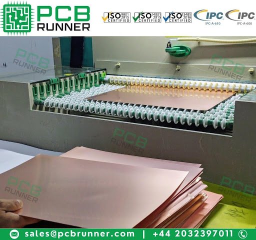
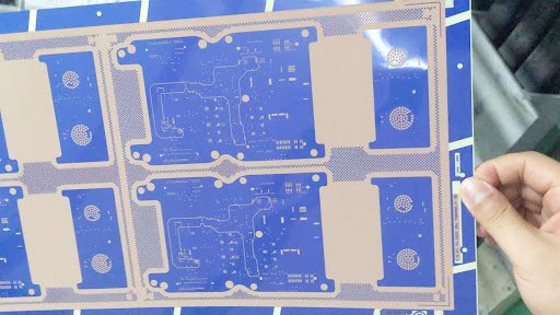
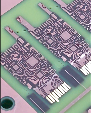
PCBs are made up of two main components: printed wires (the copper traces) and a substrate, or the board.
Substrates that divide the different layers are needed for multi-layer boards. The substrate acts as both an electrical insulator between conductive portions and a structural support for the printed wires and circuit components.

PCB substrates are incapable of conducting electric currents. They act as a layered electrical insulator between electronics for this reason. A material that does not conduct when subjected to an electrical current is known as an electrical insulator because its internal electric charge does not flow freely. As a result, plated through holes are used to connect traces on opposing levels in every layer of the circuitry.

Multilayer PCB Substrates can be used in an extensive range of electronic devices.

Purpose of PCB Substrate

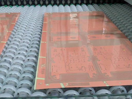
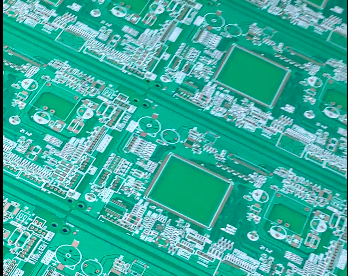
A printed circuit board is constructed using substrate as a base. A PCB’s electrical, thermal, and physical characteristics are determined by its substrate. Typically, substrates are dielectric composite structures made of epoxy resin combined with one or both sides connected with copper foil. The copper layer is then covered with a solder mask to shield it from other elements that can damage the copper traces.

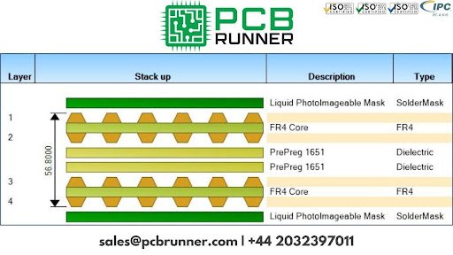
In multi-layer PCB, the laminate core is press between the substrate and all of the layers are bonded together with prepregs by applying high pressure and high temperature.

A PCB’s hard substrate enhances its strength and durability, whereas flexible substrates enable the construction of flexible circuits that may be bent and twisted without impairing signal flow. A PCB’s substrate determines its physical qualities.

Types of Multilayer Rigid PCBs Substrates

There are five different types of multilayer rigid PCBs substrates, each with special qualities for use in particular applications. 

FR-2

This lower-grade substrate is composed of easily machined impregnated paper, sometimes known as phenolic, over a fiberglass substrate. Flame Resistant is what the name “FR” stands for. Typically, less priced consumer gadgets use this kind of substrate.


FR-4

Fiberglass substrates consist of a flame-resistant substance that has been impregnated into woven fiberglass. Although the material is stiff and can be drilled, cut, or machined, tungsten carbide tools are required since the fiberglass is abrasive. In comparison to a FR-2, a FR-4 substrate is stronger and more resistant to breaking or shattering and are typically found in more expensive devices.

RF (High frequency)

RF substrates are used in printed circuit boards for high power radio frequency applications. They are made of low dielectric polymers. The substrate exhibits remarkable electrical performance properties despite its weak mechanical attributes.

A dielectric is inserted between a copper layer and a sub-composite that has already undergone lamination as part of the sequential lamination process.

Sequential lamination can be used to incorporate buried and blind vias into a PCB. A PCB with buried vias is produced by first creating a layer with blind vias (as though it were a two-sided PCB) and then consecutively laminating this layer with an inner layer.

HDI boards go through this process more than once when varying via structure types and layer combinations are required.

PCB runner has the capability of following material for multilayer PCB substrates:

PCB Material/Substrate

Description Standard Advanced
Regular TG FR4 140TG
High TG NANYA NP175, ITEQ IT180TC, IT180A
High Speed  ISOLA 370HR, FR408HR, I-Speed, PANASONIC M6, M7, ARLON 85N (PI)
RF & Microwaves ROGERS 4350B, 4003C, 4450F , ROGERS 4835
Aluminum Substrate VENTEC 4A2H – 2.2W/mK, MOT 105
ARLON 92ML – 2.0W/mK, MOT 90
Halogen Free NANYA NPG series (151, 170D, 186)

Thermal Benefits of PCB substrates
The electrical and thermal properties of PCB substrates:

A printed circuit board’s electrical and thermal conductivity are also determined by its substrate.

Important Thermal Characteristics:

The temperature at which a substrate material changes from a stiff to a soft state—or, to put it another way, melts—is known as the glass transition temperature (Tg). PCB boards should never run over the substrate’s glass transition temperature.
The temperature at which the PCB substrate material undergoes chemical breakdown is known as the decomposition temperature (Td).

Coefficient of Thermal Expansion (CTE):

CTE is a measurement of how quickly a material expands in the presence of heat. The enlargement will result in a size rise that could potentially cause internal stress and harm. To find out more about CTE, go here.

The rate at which a material conducts heat is determined by its thermal conductivity or k.

How Thermal Conductivity Affects PCB Temperature?

One of the many crucial elements of PCB design is selecting a substrate with an appropriate thermal conductivity. Smaller boards with fast-switching active components are more likely to require thermal management in PCBs, as are boards carrying high currents because resistive losses in a trace cause heat to be generated, which then transfers into the substrate.

It can be necessary to select a substrate with increased thermal conductivity if there is a likelihood that the board will produce a lot of heat while operating or if it will be used in a hot environment. Maintaining the temperature of crucial components within their acceptable operating range may also require the use of passive cooling, active cooling, or both.

Evaluating Other Material Properties and Thermal Conductivity

Strong heat conductivity PCB substrate materials are known to have strong electrical conductivity as well. This does not imply that the substrate’s actual part of the dielectric constant will likewise increase in value. Instead, it indicates that higher thermal conductivity substrates typically have larger conductive losses in their substance.

This indicates that heat at the trace’s surface and leakage between the transmission line and its reference conductor will cause losses along a transmission line in a PCB to grow. 

Volumetric expansion of Multilayer rigid PCBs substrates

The volumetric expansion of PCB substrate is another thermal factor to consider. While not all materials have a thermal conductivity that increases with volumetric expansion coefficient, it is still preferable to choose a substrate with a higher thermal conductivity since it transfers heat away from heated components and results in a more even temperature distribution across the board. This inhibits the creation of hotspots and localized volumetric expansion around active components or high-current traces.

If these traces have an extremely high current, they can be dangerous.

PCB Thermal Management for Various Applications

Higher thermal conductivity substrates help with thermal management and passive cooling, which lowers board temperatures in industrial electronics, automobile applications, cellphones, and other applications. This makes it possible for heat to dissipates more frequently over the PCB, resulting in a temperature distribution that is more uniform. To control the temperature rise, various other basic passive cooling techniques or active cooling parts can be employed, such as thermal pads (Epoxy fileed, copper paste filled or copper coin filled), heatsinks on critical components, cooling fans, arranging multiple planes in inner layers, and by choosing good thermal insulation material (HITG).

Materials for Ceramic PCB Substrates

Ceramics have far better heat conductivity than FR4, PTFE, and polyimide, but at the expense of higher manufacturing costs. Multilayer manufacturing is challenging due to the difficulty of drilling these mechanically robust substrates, both mechanically and with lasers. Since the nanoparticles of these materials will sinter at the same temperatures as ceramic PCB substrates, ceramic PCB substrates can likewise be utilized with sintered gold or silver conductors with ease. 

For heatsinks, thermal paste vs. thermal pads

Heatsinks serve as a big reservoir to trap heat and transmit it to the surrounding environment. There are two ways to attach heatsinks to active components: thermal paste and thermal pads. A heatsink needs to be mechanically fastened to its component, or it can be bonded with thermal paste or a thermal pad. While thermal paste will outlast any thermal pad in terms of wear and tear, different pastes offer varying degrees of heat dissipation. These materials also allow for the combination of a heatsink and fan to provide powerful cooling directly to active components, such as CPUs, GPUs, FPGAs, and other components that switch quickly.

Dynamic Power Regulation

This technique, which is commonly used in mobile devices too small for active cooling, involves actively turning various functional blocks on and off as needed, as well as putting components like microcontrollers into sleep mode to conserve power and get rid of a heat source in the system. When combined with some special substrate material or metal core PCB, one can make up for the low thermal conductivity of standard PCB substrates.

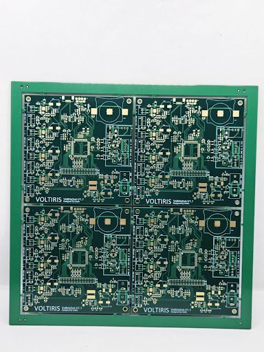
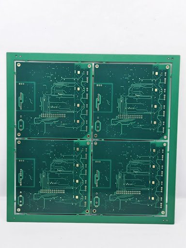
Two fundamental types of boards with only one or two layers of conductive materials over the substrate are single-layer and double-layer PCBs. Multi-layer printed circuit boards are well-suited to satisfy requirements for increased routing space or signal integrity. Multilayer PCBs, as opposed to single- and double-layer PCBs, stack several layers of conductive and insulating material to produce an intricate web of connections. Prepreg, substrates, cores, and copper layers are usually included in the stack-up. In PCBs, there are two different kinds of insulating or dielectric materials: prepreg and core.

Conclusion

After reading about PCB substrate, you may be unsure about where to make your purchase. A PCB substrate may not always need to be purchased separately. You can discuss your needs with a PCB manufacturer, like PCB Runner, by getting in touch with them. In order to jointly determine which Multilayer rigid PCBs substrates best suits your needs, you can have a discussion. In this sense, PCB Runner will be beneficial. There is an abundance of possibilities available to you due to the various varieties of PCB substrate. You may be confident that the FR-4 substrate will allow you to create a variety of circuit boards. If none of the possibilities on this list appeal to you, you may always ask us for suggestions.

High-Quality Special Material PCB Manufacturing Services for UK and Europe

High Production Volume, High Quantities of PCBs

After the verification of prototype, do you intend to produce PCBs in big quantities and at high volume? Over the years, PCB RUNNER has established a solid reputation with both local and international clients, earning them the trust of those looking for a dependable PCB fabrication service and an expedited PCB prototype. We can create stiff boards with 1–30 layers, flexible printed circuits (FPCs) with 1–8 layers, rigid–flex boards with 2–20 layers, and metal core PCBs (MCPCBs) with 1–4 layers, either with or without laser drilling microvias technology. For clients with specific or varied service needs, PCB RUNNER, a UK and EUROPE -based all-in-one PCB solution supplier, additionally offers PCB design, assembly, functional testing, and reverse engineering services. 

In  material selection and PCB production following manufacturing issues might occur: 

Materials: Certain materials work well for certain circuits when it comes to the materials required to create a PCB, for example. Ultimately, they won’t offer the optimum signal integrity performance if alternative materials are specified in the board layer stack ups. Additionally, there are instances where the materials needed for the design aren’t economical to manufacture or appropriate for the board’s working settings.

High-Quality Special Material PCB Manufacturing Services for UK and Europe - best performance, best rates

The greatest method to guarantee error-free production is to work with a quality CM to optimize your design. You’ll find that they are an excellent source of DFM information. 

To accomplish this, your CM must to have a group of engineers who can check your design for DFM problems and offer suggestions for improving production. A group of component engineers should also be able to examine your parts, so you won’t be caught off guard by any that are unavailable or not advised for production.

Naturally, there may be instances in which you have a board that needs to be manufactured quickly for a proof of concept, product demo, or prototype, and you won’t have the time to work through all of the DFM concerns. Thankfully, the majority of CMs can assist you by utilizing what you already have. Sometimes the CM can adjust quickly. At times, during production, they will make impromptu corrections to manufacturing issues. The true secret is to collaborate with them in advance and address as many DFM concerns as you can in the original design to minimize the amount of cleanup that needs to be done afterwards.

To avoid typical PCB manufacturing issues, collaborate with a CM who possesses exceptional ability to fulfill your requirements. Selecting a partner with the appropriate experience and knowledge will guarantee that even the most challenging PCB designs are constructed and finished to your satisfaction.


PCB Runner as a leading provider of special material PCB manufacturing services

PCB Runner has been the top PCB manufacturing and PCB assembly service supplier in the UK and Europe for over a decade. As quick turn manufacturers, we specialize in both small and large production numbers. We meet the requirements for IPC Classes 2, 3, and 3A and have an ISO9001 certification. PCB Runner provides printed circuit boards of the highest caliber, dependability, and prompt delivery to a variety of industries. Whether they are in the military, aerospace, defense, medical, or any other area with vital applications, our customers depend on us to provide PCBs. One of the few UK-based PCB manufacturers and PCB assembly service providers is PCB Runner.

  • Trusted PCB Provider in Europe and the UK
  • 24 Hour Tech Support Using PCB Runner
  • High-Grade PCB Manufacturing in the UK and Europe
  • Get A Free PCB And Assembly Quote Right Now

Our Abilities

  • Stiff PCBs
  • Flexible PCBs
  • PCBs that are rigid-flexible
  • PCBs using High Density Interconnect (HDI)
  • PCBs with many layers
  • PCB prototypes

Process followed for special material PCB design and production

Analyzing requirements and choosing components

Analyzing the requirements and choosing the right components, such as the CPU and power supply, is the initial stage in PCB design. Design a blueprint that satisfies every need.

Front end design within the system

PCB design software is first used to create PCB layouts. Commercial software for PCB design includes Altium Designer, Autodesk EAGLE, KiCad EDA, and OrCAD. A PCB schematic Gerber file is often the result of this design. Copper tracking layers, drill drawings, component nomenclature, and other parameters are among the data encoded in gerber files.           

Leading the Way in PCB Innovation with High-Quality Special Material Manufacturing for the UK and Europe.                                    

Photo tool Launch

Before beginning the production of circuit boards, the Design for Manufacture (DFM) check must be performed. This is to prevent design inconsistencies. Subsequently, a laser printer/plotter is used to image the PCB onto a photo film. Accurate registration holes are punched into each film sheet to align the various layers of the PCB picture film. The purpose of the film is to assist in the creation of a copper path figure.

 Inner layer printing

The substrate is taken, chopped, cleaned, and dried. It is often a composite epoxy substrate. The substrate has copper pre-bonded to both sides of it. The most crucial element in preventing short circuit or open circuit problems is panel cleanliness. 

From Concept to Creation: Precision and Excellence in High-Quality Special Material PCB Manufacturing for the UK and Europe.

Removing the undesired copper with etching 

After that, unhardened copper material is removed from the panel by washing it in an alkaline solution. Beneath the photoresist layer that has solidified, the desirable copper layer is completely shielded. After that, the photoresist covering the copper layer is likewise taken off. Thus, the only copper layer that remains intact is the necessary one.

Punching registers to align layers

Registration holes are created by aligning and visually punching the various layers. The inner and outer layers will line up as a result.

Optical inspection carried out automatically

Errors in inner layers cannot be corrected after lamination. Therefore, prior to bonding and lamination, the panel is put through an automated optical inspection process. Using a laser sensor, the device examines the layers and, if any inconsistencies are found, lists them by comparing them to the original Gerber file.

Build up and Connect 

An aluminum press plate holds the PCB panel’s layers together. Copper foils are pressed over the original layers of a double or multiple later PCB, with insulating layers positioned in between, and the etching process is repeated. Ultimately, the PCB panel receives its final shape from the lamination of all the layers together.

Drilling 

Next, holes are drilled into the PCB stack. The electronic components of the PCB, including the via holes, are supposed to be positioned and connected in these holes. A drilled hole has a diameter of between 100 and 150 microns. Drilling is an exact technique that requires precision. To attain accuracy, one can utilize X-Y coordinate systems or laser locators.       


Platting and Copper Deposition 

After drilling, this procedure involves applying a new layer of copper to the entire panel. It covers the nonconductive materials that were exposed following drilling and also ties the panels together. For plating, a chemical electrolysis setup is employed. To guarantee correct connection, approximately 25 microns of copper are inserted into the drill holes.

Copper etching and outer layer imaging

A photoresist material is put over the outer copper layer, just like in step 3, and they are then photographed. The excess copper is removed, and a protective tin guard coating is placed over the necessary copper region. This is followed by the establishment of PCB connectors.

Application of Solder Mask

After cleaning the board, the solder mask is put on. The purpose of the solder mask is to shield the board from corrosion and copper oxidation. Applying an epoxy and a solder mask together gives the board its typical green hue. UV light exposure removes unwanted solder mask. The board is then cooked in the oven.

Silver or gold surface polish

After that, the PCB is plated with a hot air solder leveling finish or lead-free HASL in gold, silver, or bronze. This protects the copper and makes it possible for the components to be soldered to the pads that are made.

"Precision and Excellence: High-Quality Special Material PCB Manufacturing for the UK and Europe


The silkscreen

The process of printing all of the important information on the PCB, including component numbers, manufacturer identification, company name, and debugging locations, is called silk-screening or profiling. This is helpful for maintenance and repairs.

Conduct an electrical test

Probe testers are used for electrical testing. Tests for both open and short circuits are run. Functional reliability is ensured via electrical tests. Functional tests are followed by durability testing.

Transforming Electronics with Precision and Excellence: High-Quality Special Material PCB Manufacturing for the UK and Europe.

V-Measuring 

The fabricated panel is cut to reveal the real PCB. PCBs are cut to precise dimensions and forms in accordance with the customer’s design and the original date on the Gerber file.
The board may be readily removed from the panel thanks to the V-cuts created along its sides.

Packing and final examination 

PCBs go through a quality and final visual check. Test results are given to customers for validation. To avoid any physical damage to the boards, the packaging is either vacuum sealed or airbag/air pocket packaged.

Quality of PCB Manufacturing 

During the process of fabrication and assembly, quality requirements are maintained by: 

  • Statistical process control monitoring rates of scrap and defects 
  • Thorough inspection verifying the output of the operation 
  • Frequent machine calibration and maintenance 
  • Adherence to strict industry standards such as ISO and IPC 
  • Tight supplier quality control procedures 
  • Supervision of the manufacturing floor environment for quality assurance 
  • Thorough examination of the completed boards, in-process materials, and raw materials 
  • Initiatives for continuous improvement to reduce flaws 
  • Quality control guarantees dependable, consistent PCB production.

Applications of Special Material PCBs

Medical area

The following are a few typical medical PCB devices: Medical imaging systems: CT, CAT, ultrasound scanners; monitors: blood pressure, glucose, and heart rate monitors; and the computers that gather and interpret these images.
insulin and patient-controlled analgesia pumps are examples of infusion pumps. inside gadgets, such as pacemakers. PCB contributes significantly to raising the standard of medical care by providing tools and equipment that help physicians discover problems and increase their accuracy and efficiency. 

End-user devices 

Flexible printed circuit boards, or FPCs for short, are a type of PCB made primarily of polyester or polyimide film. FPC gains popularity with its high density, light weight, thin thickness, bending resistance, flexible construction, and resilience to high temperatures under the trend of intelligent and thin mobile electronic products. The following consumer electronics include PCBs. Communication devices, such as radios, tablets, smartphones, and smartwatches. Entertainment systems include stereos, video game consoles, and televisions. home appliances, such as coffee makers, microwaves, and refrigerators. 

Aerospace sector

The aerospace sector has more stringent specifications, requiring PCBs to be durable and resistant to oxidation. The primary USB of any operating system used by the aerospace sector is the PCB assembly with heat management. The PCB heat dissipation design can be implemented using a compact architecture for heat dissipation. Heavy-duty, highly tailored PCBs are essential to electronic equipment used in aircraft. In the aerospace sector, PCBs are used in the following ways: power: satellites, control towers, and airplanes;  accelerometers, pressure sensors, and communication equipment as surveillance tools.

Applications for the military and defense

PCBs are used in many different applications, such as computers, guns, cars, and communications equipment. Military equipment frequently uses materials like copper, aluminum, and high-temperature laminates. The applications are listed below. Radio communication systems are examples of communication equipment. Control systems, including missile detection and radar jamming systems.  

apparatus: monitor

Quality and Compliance

In the electronics manufacturing sector, PCB Runner, a seasoned provider of expert PCB creation services, has over ten years of experience. The majority of the businesses we manufacture PCBs for are global in scope and have been with us since the beginning. We work hard to keep our clients’ satisfaction levels at or above 99%, and we take pride in offering the best service available. We are able to adapt to our clients’ changing needs because of our flexibility. Because we are adaptable, we can work with the most precise, efficient, and economical design and manufacturing methods.

Engineers, designers, R&D innovators, product managers, supply chain/manufacturing specialists, sales/customer service representatives, and quality assurance workers make up our multinational team of professional experts. 

Our production facilities are of the highest caliber, and we have synchronized our quality processes and technology roadmaps to meet the requirements of IPC Class 2, 3, and 3A. We are also accredited for ISO9001.

Why Choose PCB Runner for special pcb design

The Netherlands-based PCB maker is aware that every client and their needs are unique and distinct. Customers need to be able to trust their source to fulfill their needs, in our opinion. Our specialty is assisting clients in launching their goods into the market as quickly as feasible.

One of the rare businesses that actually manufactures boards in-house is PCB Runner. We manufacture every kind of board, including:

    • Aluminum-based metal PCBs 
    • PCBs using Rigid-Flex (FR-4 and Polyimide) 
    • Board flex (polyimide) 
    • Through-Holes, SMT, BGA, and other HDI boards 
    • Lead-Free Boards that Comply with WEEE and RoHS 
    • Intel PCB Mil spec (IPC Class 1, 2, 3). 
    • 40+ layer multi-layered circuit boards 
    • Materials for Boards: FR-4, Polyimide, Rogers, and Others 
    • Spacing and Trace to 3 mils 
    • Blind and Buried vias 
    • Filled vias Boards with Heavy Copper Via-in-Pad
    • Skilled Assembly and Fabrication Services

In addition to the aforementioned, we provide professional manufacturing and assembly services for:

  • Prototype circuits 
  • Board Runs
  • Small and Medium 
  • Quick Turn PCBs 
  • Burn-In for Boards

Conclusion 

Based on actual production procedures, this in-depth manual took readers step-by-step through the whole PCB manufacturing process, from initial schematic design to factory fabrication, assembly, testing, and inspection. Electrical engineers creating boards for mass production will find it useful to have a clear understanding of the process.

Important lessons learned include designing PCBs with manufacturing in mind, producing high-quality design data, interacting with fabrication and assembly partners in an efficient manner, and maintaining strict quality control to guarantee sturdy boards that are prepared for product installation. Electrical engineers may reliably and efficiently turn concepts into actual products by adhering to this PCB production strategy.

PCB Runner offers custom design layout services for all industries and critical design requirements. Our expert design layout team efforts help the end R&D / product engineers to reduce there time by being back & forth to design PCB based on manufacturing capabilities & running DFM & DFA twice. Please do submit your schematics & BOM files to our email at sales@pcbrunner.com or engineering@pcbrunner.com.

PCB Manufacturing Process Tolerances

The process’s stability and dependability are key components of PCB manufacturing’s success. Strict tolerances must be upheld throughout the manufacturing process in order to accomplish this. Tolerance in the context of PCB fabrication describes the maximum permitted departure from a given value. A circuit track/trace width, for instance, may have a tolerance of +/- 0.005 inches. This indicates that there is a maximum variation of 0.005 inches in the trace’s width. In PCB fabrication, tolerance is crucial because it guarantees that the final product will perform as planned. Tolerance can be impacted by a number of variables, including design specifications, production procedures, and material qualities. It goes without saying that tolerance management is essential to the PCB manufacturing process’s success. 

PCB manufacturing process tolerances


Why is the thickness tolerance of PCB boards important?


Maintaining dependable and constant performance is why PCB board thickness tolerance is important. In the event that the board thickness deviates from the tolerance range, problems with functioning and assembly may arise. Respecting industry standards can increase consumer satisfaction and the product’s perceived trustworthiness, while accurate thickness tolerance guarantees correct fit and lowers the possibility of harm. 

Recognizing tolerances in PCB fabrication

Electronic device performance is guaranteed to be consistent and dependable when PCB fabrication tolerances meet industry requirements. The permitted variation in thickness that may result in fitting issues and impact electrical characteristics is referred to as the PCB thickness tolerance. Ensuring device compatibility and achieving design criteria during production necessitates maintaining the desired tolerance. It is necessary to adhere to legitimate IPC guidelines and other quality control methods. Applications with extremely high requirements may be difficult to satisfy if suppliers and customers are misinformed about smaller tolerances. Consultations with experts can assist in overcoming even the most difficult design obstacles.

Tolerances for copper width and spacing.

For PCB board manufacturing to be successful, precise copper width and spacing tolerances must be maintained. In extremely demanding applications, signal distortion, overheating, and short circuits can be avoided by following legitimate IPC requirements and making sure that the copper width and spacing stay within the intended tolerance range. To determine whether reducing tolerances is feasible, suppliers should be consulted. Errors in the finished hole size, annular ring, or copper weight might result from miscommunication during the layout phase. Complying with the correct dimensions for the hole, pad, v-cut, and plating thicknesses can meet even the most difficult design problems without sacrificing component overages.

Annular Ring Tolerance


Annular Ring Tolerance


 Pcb Hole size Tolerances


 Pcb Hole size Tolerances


Tolerances for PCB drilling

Achieving optimal control over PCB drilling tolerances is essential for producing printed circuit boards (PCBs) of superior quality. It impacts the device’s overall functioning and component performance, in addition to tolerances for multilayer board thickness and copper width and spacing. PCB makers must follow legitimate IPC requirements or internal tolerance guidelines as smaller tolerances become required for extremely demanding applications. Boards can satisfy even the most difficult design issues if they meet all the requirements, such as completed hole size, pad size, and annular ring.


PCB Manufacturing Process Tolerances


PCB runnermanufacturing capability to acheive minimum drill hole size of 0.2mm and maximum hole size of 10mm with PTH tolerance ±3mil and NPTH ±2mil.

Tolerance for thickness of multilayer boards

For printed circuit boards with multiple layers, maintaining the thickness tolerance correctly is essential (PCBs). Variations in the board’s overall thickness could result in issues with heat dissipation and signal interference, which would ultimately impair the functionality of the device as a whole. When creating multilayer PCBs, the producer must follow stringent instructions and have appropriate control over variables like the quantity of layers and copper weight. When creating a multilayer circuit board layout, internal standards regarding board fabrication tolerances should be taken into consideration. It has become essential to meet design specifications; therefore, for feasibility consultations, a copy of the IPC Guidelines is helpful.


Tolerance for thickness of multilayer boards  

PCB design with controlled impedance tolerances


For electrical equipment to perform as well as possible, controlled impedance tolerances in PCB design are essential. Deviations from the required thickness may result in problems with signal integrity that could have a major effect on performance as a whole. To achieve smooth integration and efficiency, it is also crucial to assure optimal compatibility with other components and manufacturing processes. Throughout the manufacturing process, ensuring consistent quality depends on adherence to industry norms and specifications. PCB runner offers ±10% tolerance for impedance it means that at 80ohm to 110ohm the circuit will provide 90ohm and 100ohm resistance respectively.


PCB design with controlled impedance tolerances


Tolerances for routing/trace & spacing in PCB manufacture


In order to guarantee that electrical gadgets operate as intended, PCB manufacturers must maintain uniform routing/trace & spacing tolerances. Deviations from the required tolerance for thickness may result in problems such as delamination or warping. Keeping accurate circuit board assembly and performance demands adherence to industry standards and guidelines. Even the most difficult design problems can be avoided by adhering to uniform routing tolerances throughout all facets of PCB design and fabrication, from layout procedures to consulting. Reducing component overages while fostering stronger supplier relationships is another benefit of achieving tighter tolerances, which also guarantee high-heat performance.

Tolerances for routing/trace & spacing in PCB manufacture

Every single one of these components has a tolerance limit once the assembly is finished. Usually, this fluctuation alludes to what is known as a tolerance stack-up. To put it briefly, tolerance stack-up is the result of placing additional tolerances on top of each other. As one might expect, if a tolerance stack-up is not appropriately addressed and controlled, it can lead to harmful functional and manufacturing difficulties.

 Tolerance stack-ups are typically used to estimate the consequences of the cumulative variation permitted by certain dimensions and tolerances in order to characterize the problem-solving process. These measurements and tolerances are usually specified on an engineering plan or design.


2 layer rigid pcb stack-up

Usually, tolerance stack-up is carried out with software that enables accurate simulations and computations of all component dimensions and tolerances. By meticulously measuring and computing each component’s measurements and tolerances, this can also be done by hand.

Tolerance Chart of PCB Runner for different PCB types

 The drilling tolerances offered at PCB runner are ±3mil along with secondary drill size ±10mm and routed slot ±0.10mm. All these are compliant with international manufacturing standards.


Tolerance Chart of PCB Runner for different PCB types


PCB runner is providing the manufacturing tolerances in compliance with the IPC-A-600 manufacturing standards.

For rigid PCBs the manufacturing tolerances offered are thickness tolerance which is about minimum -0.10mm and maximum +0.10mm. These values can vary by 10%.

Same is the case with line width tolerance offered at PCB runner which is minimum 10% and maximum 20% . Another type of tolerance includes external dimension tolerance which is ±5mil and V-cut tolerance ±5degree.

Tolerance Chart  

Tolerances in solder mask features during PCB assembly


During PCB assembly, it is essential to maintain solder mask feature tolerances correctly. Since any variance in thickness could cause warping or perhaps the circuit board to fail completely, the prescribed tolerance must be adhered to. Maintaining appropriate thickness tolerance enhances production consistency and yield rates while ensuring that parts fit correctly, and the board functions as intended. Solder mask clearance tolerance by PCB runner is standard 2.0mils and advanced 1.5mils. For outer  layers solder mask clearance offered at PCB runner 4mils standard and 3mil advanced. Our highly competitive team offers this solder mask feature during assembly process complying with the IPC-6012 standards.

Tolerances in solder mask features during PCB assembly


PCB Runner offers turnkey solutions which includes custom design layout, fabrication, components procurement & assembly labor, for all industries. Our expert design layout team efforts help the end R&D engineers/ Buyers/ Purchasers to reduce their time by being back & forth to design PCB based on manufacturing capabilities & running DFM & DFA twice. You are welcome to submit your design files to our email at sales@pcbrunner.com or engineering@pcbrunner.com.

Expert Obsolete Component Sourcing Solutions for UK and European Customers

Introduction:

Electronic parts that are no longer manufactured or distributed by the original manufacturer are known as obsolete electronic components, and the only place to find them is via distributors of obsolete electronic parts. This may be the result of various factors, such as modifications in manufacturing techniques, advancements in technology, or just a deficiency in demand. Distributors of obsolete components might offer transistors, capacitors, resistors, and other electronic components.

The expenses associated with a faulty manufacturing line vary depending on the company’s size, the industry it works in, location, the products it produces, and other factors. But when a breakdown happens, the sensation of powerlessness and frustration is universal. Finding a seasoned partner who can get replacement parts for you if manufacturing is halted or slows down is one approach to feel at ease.

PCB Runners are experts in locating and distributing out-of-production and challenging-to-find electrical components. With many years of business expertise, we have provided thousands of enterprises with current production requirements, related products, and obsolete electrical components. PCB Runner can locate any component, even an outdated electronic one, if it exists across the globe thanks to the company’s extensive global supplier network. Naturally, finding a replacement for an electronic component gets even harder after it becomes outdated. This is why you need an expert with years of expertise working with this kind of component as well as exposure to all the most recent obsolescence data. 

Obsolete Component Sourcing Solutions

PCB Runner’s Obsolete Component Sourcing Services

Obsolescence problems can result in unfavorable experiences, which can severely damage consumer loyalty and company reputation. These experiences can include missing a product, problems with the product’s quality, a lack of vendor support, or anything else. Manufacturers may stop issues from harming their customers and their business in the long run by monitoring obsolescence and making plans for it.

With information insight for your technology, sourcing, distribution, and compliance oversight, ESG strategists, and business leadership, PCB Runner’s integrated platform offers a comprehensive, data-driven approach to supply chain risk management. Our global team of professional experts consists of engineers, designers, R&D innovators, product managers, supply chain/manufacturing professionals, sales/customer service staff, and quality assurance personnel. We have world-class production facilities and we are certified for ISO9001, and qualified for IPC Class 2, 3, and 3 for which we have aligned our quality systems and technology roadmaps.

To help their clients get the best deal possible, PCB Runner makes it their goal to bargain with suppliers to get the greatest terms and quality. PCB Runner is in a great position to negotiate advantageous terms for their clients because they frequently have long-standing relationships and a history of dealing with their suppliers. PCB runner’s primary responsibility is to oversee the procurement procedure from start to finish. They are therefore essential to supply chain management, particularly for companies that depend on outsourcing or global trade.

For you to strike a fair bargain with a dependable and trustworthy sourcing agent, a committed team of PCB Runners takes on the job of assisting your company with an approach to sourcing and identifying suppliers for you to make your items.

Obsolete Component Sourcing Process

It can be difficult to get obsolete electronic parts, but don’t worry; we’ve put up a list of advice that will help you improve your chances.

Make Contact:

Getting in touch with other enthusiasts through online groups and discussion boards devoted to technology and electronics can be beneficial. Making connections with people who share your interests could lead to the discovery of new suppliers for hard-to-find electronic components as well as insightful knowledge on how to acquire them.

Go to the Local Electronics Stores:

When looking for uncommon electronic parts, don’t rule out your neighborhood electronics stores. They might be willing to order the part for you or know how to find it even if they don’t have it in stock.

Examine Internet Marketplaces:

Rare electronic parts can also be found in abundance on websites like eBay and Amazon. Before making a purchase make sure to check the seller’s ratings and reviews to be sure you are working with a trustworthy vendor.

Make Use of Part Number Lookup Engines:

By simultaneously searching several suppliers and databases, part number search engines like “FindChips” and “Octapart” can assist you in finding hard-to-find electrical parts. The search engine can take care of the rest if you just enter the part number.

Industries Served

With the help of our extensive industry and product expertise base and global supplier network, we offer complete solutions for out-of-production and obsolete electrical components. Some of the main markets we serve are as follows:

Medical:

To perform life-saving procedures, the medical industry depends on robust, high-quality electronic devices. Our staff at PCB Runners is devoted to finding dependable medical parts so that decisions involving life and death are made correctly.

Aerospace and Defense:

At PCB Runners, we are aware of the significance that part legality and quality hold for our aerospace clients. We uphold a zero-tolerance stance because of this.

Communications:

The skilled staff at PCB Runners has been putting in a lot of effort to provide sophisticated supply chain administration solutions to facilitate the digital growth of the telecom industry. We can assist telecom customers in finding parts fast, including those involved in the 5G revolution.

Internet of Things:

IoT companies have to handle intricate supply chains and acquire necessary parts to keep up manufacturing and satisfy consumer demands for electronic products. We at PCB Runners can help IOT companies quickly get tracking sensors, replacement parts, and other items. Working with an international community of suppliers of old components, PCB Runners offers a plan to keep your products manufactured even if obsolescence starts to become a problem.

Quality and Compliance

We take the following steps to ensure quality control for providing obsolete components to our clients.

Supplier assessments:

This assessment entails a methodical, ongoing assessment of suppliers. We evaluate a supplier’s ability to satisfy quality requirements consistently by looking at things like the company’s quality management systems, trade references, and accreditations.

Component inspection:

It comprises internal assessments of every electronic component that is received. Our component inspection method consists of visual examinations, dimensional checks, scrape testing, resurfacing, and other procedures.

 Supplier Qualification:

Some criteria are taken into account to qualify suppliers during the assessment process. These elements could consist of the supplier’s standing in the market, financial soundness, accreditations, quality control procedures, and conformity to industry norms.

Quality control systems:

Evaluating a supplier’s quality control systems can reveal information about how well-equipped they are to regularly deliver components of the highest caliber. To verify compliance with quality standards, this assessment may entail looking into testing protocols, inspection techniques, processes, and traceability systems.

Previous Results and Track Record:

Assessing a supplier’s prior results is essential to determining their dependability and consistency. Examining their track record of producing flawless components, their receptiveness to quality concerns, and their dedication to ongoing development are some of the tasks that may be included in this evaluation.

Why Choose PCB Runner for Obsolete Components

  • With its global part search capabilities, PCB Runner provides a high-quality, completely traceable, and quick-turnaround component sourcing service that is valued by both smaller, independent companies and some of the world’s largest brands.
  • With the use of the newest part-search technologies and a distinct network of international sourcing agents, PCB Runner can identify obsolete or difficult-to-find components far more rapidly and accurately than its competitors.
  • With our extremely efficient and reliable part-sourcing service, we will ensure that your manufacturing line continues to run while providing a completely traceable and time-sensitive supply chain solution.
  • We are aware that every client and their needs are unique and distinct. Customers need to be able to trust their source to fulfill their needs, in our opinion. Our specialty is assisting clients in launching their goods into the market as quickly as feasible.

PCB Runner offers turnkey solutions which include custom design layout, fabrication, components procurement & assembly labor, for all industries. Our expert design layout team efforts help the end R&D engineers/ Buyers/ Purchasers to reduce their time by going back & forth to design PCB based on manufacturing capabilities & running DFM & DFA twice.

You are welcome to submit your design files to our email at sales@pcbrunner.com or engineering@pcbrunner.com

Reliable PCB Part Procurement Services for UK and European Customers

As experts in the electrical sector, Pcb Runner is aware of how vital dependable and efficient component sourcing is to our business. But frequently, we run into problems that impede our procurement procedures and affect project deadlines. The article also suggests practical solutions to the top five problems encountered by experts in the acquisition of electronic components.

Depending on the PCB components required, acquiring components may need collaborating with both local and foreign vendors. It is essential to consider elements like cost, lead times, quality, availability, and minimum order quantities while purchasing PCB board components. To ensure proper operation, printed circuit board components also need to be compatible with other parts of the circuit.


Reliable PCB Part Procurement Services for UK and European Customers


 To put it briefly, obtaining electronic components is essential to the electronics sector because it guarantees the dependability and safety of the final goods.

Challenges of Procuring Electronic Components and Parts for PCB Projects 

The challenges of procuring electronic components and parts for PCB projects are given below :

Disruptions to the Supply Chain:

 Natural catastrophes, geopolitical events, and market volatility are some of the causes that can cause disruptions to the global supply chain. Electronic component shortages, delays, and price increases may result from these interruptions.

 Cost management:

 When purchasing electronic components, striking a balance between cost and quality is a recurring difficulty. The total cost of components might be affected by price changes, market needs, and shifting exchange rates.

 Component Obsolescence:

 As technology advances, manufacturers discontinue products, or consumer demand shifts, electronic components may become outdated. Planning ahead and using mitigation techniques are necessary to deal with component obsolescence.

 Quality Assurance:

 To prevent product failures and expensive rework, it is crucial to guarantee the quality and dependability of electrical components. The issues associated with quality assurance are non-conformance of products, counterfeit components, and varying quality standards.

 Regulation and Compliance: 

Certain components, such those covered by RoHS (Restriction of Hazardous Substances) and REACH (Registration, Evaluation, Authorization, and Restriction of Chemicals), may be subject to regulations and compliance requirements. When acquiring electronic components, it is crucial to take these restrictions into account as they may affect the pricing and availability of components.

 Although there are many distributors of components, only a select handful can be relied upon to provide high-quality products. When looking for component wholesalers, manufacturers of printed circuit boards typically worry about which company would provide the greatest service. Selecting a business that can handle any problem related to part procurement would be a smart choice. Leading component distributors are equipped to handle any challenge. These include finding the difficult-to-find and obsolete parts and meeting tight deadlines. Collaborate with businesses that employ certain systems for data collection as well. In order to learn more about these businesses, you may also conduct additional research about them online.

 PCB component sourcing and procurement are crucial phases in the product development lifecycle that call for a thorough evaluation of supplier capabilities, component quality, lead times, and supply chain robustness. Building strong ties with trustworthy distributors and suppliers of components is crucial to obtaining a steady supply of high-grade components for electronic production.

 With over ten years of professional experience in the high-tech electronics manufacturing sector, PCB RUNNER LIMITED offers One Stop Service for quality PCB production and assembly on prototypes and scale volumes. For businesses worldwide, we offer Design Layout, PCB fabrication, parts sourcing, and assembly services. The majority of our clients have been with us since the beginning.

 Below mentioned are some trusted component suppliers across the Europe and UK. 


The fact that PCB Runner has specialists for every step of PCB assembly and manufacturing is by far our greatest asset. We provide PCB fabrication and assembly services that are full turnkey, partial turnkey, and full feature. To put it briefly, we provide a comprehensive end-to-end solution for your projects. From design and manufacturing to assembly, testing, packing, and shipping, our professionals will be at your side every step of the way.

You will quickly see the benefits of working with PCB Runner for your PCB fabrication and assembly since they are a one-stop shop, saving you the trouble of contacting multiple businesses to finish your project.

We are able to adapt to our clients’ changing needs because of our flexibility. Because we are adaptable, we can work with the most precise, efficient, and economical design and manufacturing methods.

Engineers, designers, R&D innovators, product managers, supply chain/manufacturing specialists, sales/customer service representatives, and quality assurance workers make up our multinational team of professional experts.

 Phases of the Acquisition of Electronic Components

Prior to sourcing electronic parts, the steps listed below must be followed carefully:

Acquisition of Requirements:

 Have a clear idea of the components you need for your project, including their specs, the quantities needed, and the anticipated delivery date, before you begin your search for them.

Selecting Suppliers:

Selecting a trustworthy supplier is necessary to guarantee the timely and high-quality delivery of components. Prior to making a purchase, consider the supplier’s standing, background, and performance. You can also read through the supplier’s customer reviews.

Examine Prices and Quality:

 After you’ve found reputable vendors, evaluate their offerings to decide which is best for you. Additionally, look for any hidden expenses or any extra charges, such as shipping or handling fees.

 Online Sourcing Platforms:

 A large number of online sourcing platforms give a comprehensive range of product details, including technical specs and datasheets, along with a comprehensive selection of components. They are great sources for locating and contrasting parts from various vendors. This can assist you in researching the market.

 Look for Alternatives:

 Consider other possibilities if your favorite provider does not have a certain component in stock. For example, you might be able to use a part that is comparable to what you need or from a different manufacturer.

Lead times:

 Lead times can significantly affect a project’s total timeline. Make sure you give yourself enough time for delivery, and if your application calls for it, think about ordering parts ahead of time.

 Advanced Techniques and Resources Used in the Procurement Process

 To minimize the effects of unanticipated events, tight collaboration with suppliers is necessary to forecast component requirements, optimize inventory levels, and create backup plans for possible supply chain interruptions.


Additionally, utilizing digital platforms and technologies for component sourcing and procurement, like online marketplaces, supply chain management systems, and electronic component databases, can improve transparency, expedite the sourcing process, and enable effective supplier communication. Adopting digitalization in the procurement of components might result in notable advantages concerning supply chain agility, risk mitigation, and cost optimization.

 PCB Component Testing and Quality Assurance

The overall functionality and lifespan of electronic systems depend heavily on the quality and dependability of PCB components. Strict quality control procedures must be followed during the manufacturing and assembly stages in order to identify and stop component flaws, non-conformities, and performance variations.

 Advanced testing methods are used to evaluate the durability and functional integrity of PCB components under a range of working situations. These methods include vibration testing, thermal cycling, electrical testing, and environmental stress screening. These tests verify the functionality of components in a variety of real-world settings and assist in locating potential flaws or vulnerabilities in them.

To make sure that sourced components fulfill the necessary specifications and industry norms, quality assurance procedures including incoming inspection, traceability, and compliance verification are essential in addition to functional testing. The adherence of components to performance and regulatory requirements is validated by certifications such as ISO quality management, RoHS compliance, and industry-specific certifications.

 Working together with independent validation authorities and recognized third-party testing labs can give another level of assurance to the dependability and quality of PCB components. To promote improvements in component quality and dependability over time, component suppliers must be included in feedback loops and continuous improvement programs.

 Sectors Accessed by PCB Runner

PCB Runner has been working with clients for more than ten years to produce top-notch products and services that meet a range of market needs. We take pride in our ability to deliver projects on schedule and under budget. Printed circuit board (PCB) design is one of our specialties; we combine mechanical, signal, and power engineering to PCB layouts to produce prototypes quickly. Our primary focus is on creating dependable printed circuit boards (PCBs) for a diverse range of sectors, such as:

 Applications in the Military and Aerospace, Healthcare and Medical Electronics, Telecommunication and Networking, and Industry , Applications for Consumer Electronics in Automotive.

 Aerospace

 We have been providing services to the aerospace and defense sectors. In addition, we offer related services and PCB design for aviation electronics, control systems, wearables, weapons, communications, and in-flight entertainment applications. Additionally, we provide production support for modern applications such cars, avionics systems, ruggedized systems, and power supplies. It’s also in communications, countermeasures, helicopter parts, and cockpit lights.

Due to their lengthy development cycles and high qualification costs, aerospace companies need to find partners that can provide solid, dependable, and reasonably priced products.

 Medical Electronics and Healthcare

Among our esteemed clients, PCB Runner is one of the top producers of PCBs for medical and healthcare equipment worldwide. We offer PCB design and manufacturing services for image scanning systems, surgical devices, laboratory, dentistry, and medical equipment to the healthcare and medical electronics industries.

 PCB Runner’s custom-built PCBs for engineered products are of the necessary caliber and dependability. Our PCBs are used in medical equipment used by industries all over the world for vital functions like patient diagnosis.


What Identifies Us Different

Our PCBs are specified by original equipment manufacturers in the healthcare and medical sector for use in their products, which include gas chromatographs, computers that interpret ECG arrhythmias, ENT diagnostic tools, blood analyzers, gas analyzers, ECG transmitter/receiver units, pacemaker analyzers, biopotential analyzers, heart rate monitors, and more. Our medical customer list includes a number of globally recognized producers of medical devices.

 Networking and Telecommunication

 PCB A wide range of printed circuit boards are designed and produced by Runner for the networking and telecommunications sector. We provide component sourcing for rigid, flex, rigid-flex, and HDI type PCBs. Our PCBs are used in base stations, carrier networks, access networks, routers, satellites, radios, fiber-optics, mobile and broadband communications, and video, voice, and data equipment by the telecommunication and networking sector.

Reliable PCB Part Procurement Services for UK and European Customers


Uses in Automotive

Because automotive PCBs must endure extreme heat and vibration as well as exceed lifespan standards, PCB Runner’s experience with PCBs component sourcing for these applications enables them to solve the industry’s demands. Zero-defect products are needed for automotive applications; PCB Runner provides high-reliability PCBs for these applications.

 Quality PCB component sourcing in UK & Europe

 PCB Runner does not operate as a broker; instead, we review all of your engineering files prior to moving forward with Custom PCB fabrication—we do not charge for the review—and we make sure our customers receive what they expect. We have our own state-of-the-art manufacturing facility for providing the consistent quality our customers need. We also offer after sales service to quickly handle any questions or problems of our customers.

Certifications and Registrations for PCB Runners

 APPROVALS

We withhold a number of PCB certifications as a symbol of our dedication to the quality management system, demonstrating our steadfast commitment to upholding standards of quality. .

The 2015 ISO 9001 standard

ISO 14001:2015

ISO 13485:2016

 Why PCB Runner should be chosen for components sourcing

 PCB Runner provides all services under one roof as a PCB manufacturer in the UK and Europe and PCB assembly service provider in the UK and Europe. Our clients receive single-window service. In order to make it easier for our customers to work with our printed circuit board production and assembly skills, we offer exclusive services.

 Strict Quality Control

At PCB Runner, we recognize the value that PCB functionality and quality have for our clients. For this reason, we incorporate quality-oriented concepts throughout every stage of the assembly and production of PCBs. We are still dedicated to conducting all PCB-related activity in accordance with recognized worldwide quality standards.

We ensure that every one of our assembled and bare PCBs meets or surpasses the exact specifications provided by our customers. Our reputation for excellent quality, timely delivery, and competitive pricing is attested to by our client.

 The Benefit of choosing PCB Runner

For the production and assembly of fully functional printed circuit boards including component sourcing , PCB Runner is the recommended option. The diversity and adaptability of the solutions we provide are preferred by our clients. We provide every kind of printed circuit board you need, ranging from single-layer to multi-layer, rigid boards, rigid-flex boards, and HDI boards. No matter the quantity of your purchase, we can handle boards of any form or size that you require.

 Tell us what kind of boards you require, please. We are able to provide you with RoHS compliant high-temperature, high-frequency, high-speed boards, or PCBs. Our skilled engineers, designers, and fabricators can make any kind of board you require from us.

 24×7 Technical Assistance Using PCB Runner

You can count on a live person to answer your phone call when you contact PCB Runner. We promise to provide each and every one of our clients with individualized customer care. Any time of day, a CAM expert will be in contact with you thanks to our round-the-clock Tech Support.

 Get A Quick PCB And Assembly Quote Right Now

You can order or rearrange PCBs, submit files, get status information, and get immediate PCB quotations at any time of day. You can submit your files for order processing with ease, regardless of where you live—on the East Coast or in the Midwest.

 Conclusion

 Through a comprehensive comprehension and resolution of the primary obstacles in the purchase of electronic components, experts can improve their approaches to procurement, reduce potential hazards, and achieve favorable results. Adopt proactive strategies, cultivate robust supplier relationships, and capitalize on technology and market knowledge to maintain a competitive edge in the ever-evolving realm of electronic component acquisition.
Purchasing parts is a crucial step in the assembly and production of printed circuit boards. This relates to sourcing and acquiring printed circuit board component parts. There are several pieces that might be hard to locate. However, everything will be simple if you work with the top component vendors.

 PCB Runner offers turnkey solutions which includes custom design layout, fabrication, components procurement & assembly labor, for all industries. Our expert design layout team efforts help the end R&D engineers/ Buyers/ Purchasers to reduce their time by being back & forth to design PCB based on manufacturing capabilities & running DFM & DFA twice. You are welcome to submit your design files to our email at sales@pcbrunner.com or engineering@pcbrunner.com

Reliable Provider of Hard to Source Components for UK and European Customers

 In the electronics business, sourcing components is essential for locating PCB parts and other components needed to complete circuit boards and component boards. Resistors, capacitors, integrated circuits, transistors, diodes, and other components may be used in this process. In order to guarantee the quality of the product, the components must also be obtained from reputable vendors.

 Depending on the PCB components required, acquiring components may need collaborating with both local and foreign vendors. It is essential to consider elements like cost, lead times, quality, availability, and minimum order quantities while purchasing PCB board components. To ensure proper operation, printed circuit board components also need to be compatible with other parts of the circuit.

 Before being utilized in manufacturing, the circuit board parts that are purchased from suppliers need to be inspected. This involves verifying that the parts meet safety, performance, and quality standards. To make sure they comply with industry standards and laws, circuit board components must also be properly labeled, kept, and tracked.

To put it briefly, obtaining electronic components is essential to the electronics sector because it guarantees the dependability and safety of the final goods.

The Challenge of Locating PCB Components is Mostly Caused by Three Variables

1. Complicated Design Specifications

For electronics makers, there are new design problems arising from IoT devices, hardware related to artificial intelligence, and growing demand for eco-friendly equipment. PCBs for similar items frequently need:

Flexibility: Complex designs and smaller items could call for flexible printed circuit boards. Finding a flexible PCB that can handle the design is one thing, but finding one without excessive material prices and assembly steps is quite another.

Sustainability: Lead times and costs may rise as a result of the growing demand for environmentally friendly materials and production techniques.

2. Disruptions to the Supply Chain

The COVID-19 lockdowns continue to generate supply chain issues that could impede the procurement of PCB materials like copper and base laminates in numerous industries.

 Beyond the pandemic’s effects, PCB manufacture has been further burdened by the rising demand for copper in 5G devices and electric vehicles. 

3. Few Local Vendors

Depending on the location of electronics manufacturing, locating trustworthy local PCB suppliers can be challenging.
Using regional vendors has several benefits, including: 

  • Collaboration made easier
  • Reduced freight charges
  • Adaptability and reactivity

A simpler way to confirm quality controls Businesses can save time and money by locating a trustworthy local PCB provider, but the options aren’t always plentiful. It’s possible that local PCB assemblers won’t have access to the appropriate tools or materials for the job, even in the event that manufacturers do have access to such services.

The Value of Selecting a PCB Manufacturer for Your Requirements

Selecting a reliable PCB manufacturer is essential to guaranteeing the promptness and quality of your printed circuit board orders. Additionally, it aids in the discovery of novel approaches to reduce costs, particularly for original contract manufacturers. But why is it important to locate a contract PCB partner that meets your requirements?

 Pcb Runner can guarantee that the best products are being produced by sourcing all PCB parts and components from reliable vendors and guaranteeing that each component is verified and tracked.

 PCB Runner has been the top PCB manufacturing and PCB components service supplier in the UK and Europe for over a decade. As quick turn manufacturers, we specialize in both small and large production numbers. We meet the requirements for IPC Classes 2, 3, and 3A and have an ISO9001 certification. PCB Runner provides printed circuit boards of the highest caliber, dependability, and prompt delivery to a variety of industries. Whether they are in the military, aerospace, defense, medical, or any other area with vital applications, our customers depend on us to provide PCBs. One of the few UK-based PCB manufacturers and PCB assembly service providers is PCB Runner.

 PCB Runner offers comprehensive services and solutions for PCB assembly. We offer a full range of services under one roof, including component sourcing, board assembly, and testing.

Steps for Finding Hard to Source Components

1. Increased speed and precision of production

In addition to having a short time-to-market, high-quality printed circuit boards are essential for success in the PCB market. Higher quality and shorter lead times are ensured by the presence of cutting edge facilities and technology, as well as reliable, skilled, and informed ECMs. What’s more? ECMs test the boards in real-world settings while specialists keep a close eye on them.

2. Restricted design time

 The majority of manufacturers of electronic components may have concerns about the PCB design process and its timeline. It makes the time needed to fabricate and assemble PCBs worse, particularly in complex cases. Because of their extensive training and experience, an ECM can help you get through these and other challenges.

3. Receiving all necessary services from PCB firms that operate as one-stop shops

The majority of OEMs get a variety of services from their electronic contract manufacturers, or ECMs. The majority of extremely skilled ECMs offer complete PCB solutions, from conception to installation, to meet a variety of electronic applications. Therefore, if you have specific demands, like assembly, you don’t need to contact many organizations. Additionally, ECMs offer supply chain logistics that impede most OEM’s. 

4. Reduced operating expenses and increased output

It can be challenging for small and medium-sized electronic businesses to commit to the significant capital expenditure that PCB production may demand. Therefore, collaborating with ECMs can help companies ensure higher volumes and a faster time to market while also keeping their costs down.

5. Electronic component sourcing done quickly

Purchasing PCB components can be quite expensive for small and medium-sized businesses. It is therefore helpful to collaborate and have the ECM obtain the components on their behalf. Parts can be obtained by ECMs from their intricate supply chain contacts with speed and efficiency. Additionally, free part testing and inspection are provided by the ECM.

6. Saves money on costly rework

The ability of ECMs to conduct thorough testing and inspection is helpful in producing a PCB that is faultless. These methods of automated and manual testing guarantee quality and do away with the possibility of PCB rework. 

In addition to potential substitutes for those difficult-to-find parts, we’ll look at some of the greatest web tools for finding components in this post.

7. Parts and their accessibility

Usually, components are grouped according to their availability. For every component, there are typically 5 levels of availability:

1) The part is still manufactured and stocked.

2) The part is still made, however it is not available.

3) Although the part is no longer produced, it can still be available as a salvage product.

4) The part is no longer in production and won’t be available in salvage form.

5) The part is no longer in production and can only be found in salvage condition.

8. Internet-based sources for parts

Websites in the nature of marketplaces have proliferated online, providing a wide selection of parts from competing vendors. Reputable electronics websites abound and provide a vast inventory of parts that are simple to search by brand or category. Marketplaces allow customers to look at what’s available for a wide variety of products. They could aid in time savings for purchasing managers.

 9. Substitutes for difficult-to-find parts

There are still ways to locate a certain part if you need it for your project but it is no longer manufactured.

Using the PCB Runner Electronics website is one approach to locate these products. Although some of the products on this website may not be as well-known as others, they are nevertheless necessary for some types of undertakings. If you want to stay away from overspending on components and counterfeit goods, this is a wonderful solution for you.

 10. Look for Reputable Vendors

 Customers want to buy their end-of-life components solely from reliable vendors who sell authentic, certified parts. Through their online marketplace for electrical components, Pcb Runner provides that guarantee.
If you’re seeking for hard-to-find parts, stores that specialize in outdated electronics can be a good choice. Whether you need parts for the newest technology or hard-to-find, outdated, or end-of-life components, Pcb runner has them.

 Because technology is developing so quickly, electronic component obsolescence is at an all-time high. OEMs are facing significant challenges in keeping up with the ever-increasing demand for electrical components in the electronics industry due to widespread innovation.

Recognizing the Dangers of Obsolescence and Advanced Techniques for Component Sourcing

 Since every component has a finite lifespan, component obsolescence is inevitable over time. Every component eventually becomes outdated. On the other hand, component obsolescence is happening faster and faster. This indicates that you are dealing with more difficulties.

 Managing the obsolescence of electronic components

 Knowing that obsolescence is inevitable in sufficiently long a time, how will you handle the difficulty when it arises?

 Recognize the reasons of obsolescence

 Three primary factors contribute to the obsolescence of electrical components: shorter product life cycles, rising demand, and innovation. These come together to form the ideal storm. The rapid advancement of semiconductors is a prime illustration of this storm. Which obsolescence causes will have the biggest impact on you? Knowing this will help you to properly plan for the future

When creating a product, consider its lifespan

 Creating products with components that aren’t anticipated to become outdated during the course of the product’s lifecycle is the strongest defense against obsolescence.

 There are several techniques to guarantee longevity:

  •  Review the component’s “Production Status.”

 Find out from your provider how long the components last. If the datasheet was created more than a few years ago, this may be a sign that the part needs to be upgraded soon. It may take several years for a component to become obsolete, even if that is the case. Your company will benefit greatly from this understanding.

  • Discover the true nature of obsolescence

When you receive a message that a component you use is getting outdated, investigate the cause of the issue from a distance.

The PCN (Product Change Notification), which has the necessary technical information, can be examined to do this.

There’s a strong probability that you can locate a comparable component if the component is passive. You might need to update to a newer component if the old one is still functional.

When Obsolescence Occurs, how to Handle it?

When it comes to handling obsolete components, you have three options:

 Equivalency: this is the process of searching for a comparable part. Many components, including semiconductors, have cross references that allow you to locate identical equivalents. To make sure there is cross compatibility, you should check the datasheets.

 Design is the process of collaborating with an OEM to have a component manufactured on your behalf. Because the component is specific to you, there is less risk but a higher expense. Micro-controllers and NANDs are typical examples.
Use outdated stock; there’s undoubtedly a component in storage someplace in the world that you require. If you can locate it, you can get this. To obtain the components you require in this situation, an electrical component distributor is your greatest ally.

Strict Quality Control Measures and Component Verification Procedures

 PCB contract manufacturers will employ their internal technical staff to review the design and assess the component needs in order to guarantee quality from the beginning. The parts listed on the bill of materials will often be acceptable, but the evaluation will be on the lookout for the following issues:

 Performance: For some circuits, there might be better possibilities where a different component or a different design will improve the PCB’s performance.

Cost and Availability: Even though the components are high-quality, the circuit board cannot be finished if they are too expensive or unavailable.

 Component life cycle: Production of circuit boards will be impacted by parts that the manufacturer decides to discontinue before the project’s anticipated completion. Before production begins, it is preferable to replace outmoded or end-of-life parts rather than redesigning them afterwards.

Thorough engineering review is a crucial step in the entire quality control process that guarantees a circuit board is manufactured successfully. In a DFM review, the design’s manufacturability will be assessed concurrently, and the customer will be advised of any necessary modifications. The next stage of the quality control procedure will start with the acquisition of parts and materials after all inspections have been finished and any required adjustments have been made.

Applications in Sectors like Aerospace, Defense, Industrial Automation, Medical Devices

  • Applications in aerospace, defense

Electronic manufacturers in high-reliability sectors such as aerospace, medical, and military have historically placed a strong emphasis on managing component obsolescence. No sector of the electronics industry can afford to ignore its significance for long-term economic viability these days.

Numerous military and defense systems depend on electronic components that are no longer made by the original manufacturer or offered for sale by its approved dealers. These systems’ lengthy lifespans serve as one of the foundations for this dependency.

Even though an electronic component might only be produced for two years, many defense systems that utilize them might last for over 20 years. Electronic components that are older frequently require testing and retaining in order to prevent solderability problems such as tin whiskers.

These highly dependable businesses rely heavily on a technology that becomes outdated in a matter of years, if not sooner, is produced in unsafe conditions, and has little control over market dominance.

  • Applications in medical

These issues—staffing shortages, worldwide component shortages, and shipment backlogs—have only made the COVID pandemic, which is still raging in some regions of the world, worse. Massive delays and higher shipping costs were seen in almost every industry when manufacturing moved overseas.

 Specifically, the worldwide shortage of components has caused an 8–10 month delay in some orders for the medical industry. Additionally, legal and medical complications have made matters worse, and medical device OEMs have had to deal with grave worries around device obsolescence.

 The mitigation of obsolescence risk has become considerably more challenging due to shortages and bottlenecks in the supply chain. It can be necessary for certain medical device producers to schedule several years in advance to make sure their machinery doesn’t break down.

The issue of medical equipment obsolescence poses a significant challenge for healthcare organizations and practitioners.

 Choose components with long-term availability or multiple sources for all necessary parts to lower the risk of sourcing challenges and price volatility brought on by low supply or excessive demand. To guarantee a reliable supply chain, for example, opt to employ components that are frequently found in other industries, such as the automobile or aerospace industries. As a result, there is rivalry for their purchase, but it also guarantees that, as long as there is a large demand, they will always be accessible, usually from several sources. When these tactics aren’t an option, employ best practices to lower the risks associated with single-source components.

 Quality and Compliance

Certifications and Registrations for PCB Runners

APPROVALS

We withhold a number of PCB certifications as a symbol of our dedication to the quality management system, demonstrating our steadfast commitment to upholding standards of quality.

The 2015 ISO 9001 standard

ISO 14001:2015

ISO 13485:2016

 Why Choose PCB Runner for Hard to Source Components

Trusted PCB Provider in Europe and the UK

 Because we are a reputable PCB supplier in the UK and Europe, our customers continue to buy from us. We follow through on our promises, so our clients know they can rely on us. Every month, PCB Runner welcomes a number of new clients, many of whom are recommendations from happy clients. Many OEMs have come to rely on us for all of their PCB needs since we have earned their trust.

 In today’s world designer do not want to hassle for keeping track records of components and spend a lot of time to communicate with suppliers and wasting a lot of time on maintaining records. For this reason PCB runner provide best service at only 7% service charges. We are also excelling in finding out obsolete components from authorized local an off shore dealers. Below mentioned are some trusted component suppliers across the Europe and UK.


Reliable Provider of Hard to Source Components for UK and European Customers

24-Hour Tech Support With PCB Runner

 Whenever you call PCB Runner on phone, you can expect a live person to reply. We are committed to offering personal customer service to all our customers. Our 24-hour Tech Support will put you in touch with a CAM professional at any time of the day.

Conclusion

When a passive electronic component becomes more reliable, its availability in terms of value, case size, voltage, and other factors declines exponentially, while its unavailability due to stock outs or lead times climbs exponentially. When trying to construct units at every stage—from the initial concept to the finished build—this can provide significant obstacles. As a small and medium-sized OEM, the success of a PCB product in the market can greatly affect its quality and impact. To ensure this, though, one must know how to choose a reputable and top-tier PCB manufacturer and be aware of their production procedures. We hope that the information you have received has changed the way you think about the whole PCB manufacturing process.

Providers of old electrical components are essential to sectors that depend on hard-to-find parts and legacy systems. They successfully negotiate the difficulties of sourcing, authentication, limited supply, and expertise maintenance to offer consumers options that are both economical and ecologically friendly.

PCB Runner offers turnkey solutions which includes custom design layout, fabrication, components procurement & assembly labor, for all industries. Our expert design layout team efforts help the end R&D engineers/ Buyers/ Purchasers to reduce their time by being back & forth to design PCB based on manufacturing capabilities & running DFM & DFA twice.

You are welcome to submit your design files to our email at sales@pcbrunner.com or engineering@pcbrunner.com

Reliable Staggered Via PCB Manufacturing Solutions for UK and Europe

Printed circuit boards, or PCBs, are the building blocks of electronic devices because they allow signals to flow between components and provide electrical connections between them. Vias, which create interlayer connections, are one of the essential components of PCB design. One popular form of via that is essential to obtaining the best possible performance, reliability, and signal integrity is the staggered via. The purpose of this note is to examine the features, benefits, applications, and manufacturing considerations of staggered vias in detail. As seen in the figure below, they have a conical shape but are joined without overlapping to make an impressive structure.

Staggered vias are distinguished by their distinct entry and exit locations on various PCB layers.

Characteristics and Layout:

Staggered vias are distinguished by their distinct entry and exit locations on various PCB layers. In order to minimize the possibility of signal crosstalk between neighbouring vias, the entrance and exit points are purposefully spaced apart. This offset design minimizes interference possibility and preserves signal integrity while improving electrical performance.

Benefits of Staggered Vias:

Signal Isolation:

Staggered vias greatly lessen the chance of signal interference between neighbouring vias by offsetting the entry and exit sites. In high-speed applications, where preserving signal integrity is critical, this trait is very important.

Improved Electrical Performance:

Higher-frequency signal transmission is made possible by staggered vias’ reduced resistance and inductance. Improved overall electrical performance is a result of the decreased parasitic effects.

Ease of Manufacturing:

When compared to more sophisticated via types, staggered vias are comparatively easier to create. They necessitate perforating the entire printed circuit board, and the offset design is simply incorporated into the manufacturing process.

Tighter designs:

Upon closer inspection of the high-density interconnect PCB, we can see that the circuit network connections on the board are extremely intense. Because of its tremendous intensity, the board appears to require less actual physical space. The designers can create more compact constructions by utilizing design elements like tacked and staggered vias, which will increase the versatility of HDI circuits.

Reduced trace lengths:

In comparison to other regular vias,  have shorter trace lengths. The smaller dimensions and sizes of the staggered are the cause of this. Additionally, a micro via’s smaller size enhances its FR capabilities and EMS features.

Outstanding dependability:

Staggered via is far more inventive and efficient than through-hole when taking reliability into account. Compared to other vias, microvias are far more dependable, regardless of the size of the circuit board. Microvias are a dependable solution for preserving a circuit board’s thermo-mechanical dependability. Additionally, a PCB’s functionality and performance are impacted by staggered via reliability.

Encouragement of cutting-edge technology:

This is just another fantastic advantage of microvias. Staggered fit into a PCB with less room. As a result, they enable the production of compact and smaller PCBs. Compact PCBs are also now a common feature of contemporary electronics.

Manufacturing challenges of PCBs using staggered vias

Drilling:

Using a laser to drill micro vias frequently requires exact adjustment of the laser’s parameters to ensure that the holes produced are the right size and form.

Plating:

Specific plating techniques must be used to ensure that micro vias are correctly attached to the other printed circuit board (PCB) layers.

Examine:

Staggered Microvias may be difficult to visually verify, thus non-destructive testing methods may be required to ensure proper production and connection.

Selection of materials:

The materials chosen for use on the printed circuit board can have a big impact on how reliable staggered micro vias are. The materials utilized in the production of micro vias must be of a high grade.

Select Top-Rated PCB Manufacturers:

It’s critical to find a reputable manufacturer who guarantees accurate positioning of staggered vias. The best manufacturers are able to perfectly design the PCB board to fit your specifications. Their state-of-the-art and well-equipped manufacturing facility operates high-tech machinery and processes. Providing consistency and quality should be the aim of a PCB maker. Thus, deal with the PCB manufacturing company to obtain a superior product.

PCB Runner provides all services under one roof as a PCB manufacturer in the UK and Europe and a PCB assembly service provider in the UK and Europe. Our clients receive single-window service. In order to make it easier for our customers to work with our printed circuit board production and assembly skills, we offer exclusive services. Our clients pick us because we provide:

Trusted PCB Provider in Europe and the UK
24 Hour Tech Support Using PCB Runner

High-Grade PCB Manufacturing in the UK and Europe
Get A Free PCB And Assembly Quote Right Now

Pcb Runner manufacturing capabilities 

Advanced PCB Board Types


We provide a range of sophisticated PCB board kinds and HDI board types, including the following:

  • From the topmost layer to the bottommost layer, via vias
  • Blind vias connecting two or more HDI layers to a surface layer
  • Buried /staggered  amidst two or more inner HDI strata
  • Substrates that are passive and not connected electrically
  • Coreless structure with pairwise layers
  • Coreless construction alternative using a pair of layers

There are more benefits when you use our HDI boards. By simply converting their current design to an HDI board design, any innovative organization can reap the benefits of HDI boards. Manufacturer of High-Density Interconnect, PCB Runner, provides a wide range of services for converting your advanced printed circuit boards to HDI PCB design.

Buried staggered via – How Are Buried and Blind Vias Constructed?

Drilling

The multilayer lamination can be done either before or after the vias are formed. Drilling is used to add the blind and buried vias to the PCB, which might be risky. It is critical that the builder comprehends and is conscious of the drill’s depth. Insufficient depth in the hole could prevent a strong connection. However, if the hole is too deep, it may result in distortion or a deterioration of the signal. It wouldn’t work if any of these things happened.

The process of sequential lamination

A hydraulic press is used to laminate the layers of copper in a printed circuit board (PCB) together at high temperatures and pressures. The layers are separated by a fibreglass sheet that has been pre-impregnated with epoxy. Sequential lamination can be used to incorporate buried vias into a PCB. A PCB with buried vias is produced by first creating a layer with blind vias (as though it were a two-sided PCB) and then consecutively laminating this layer with an inner layer.

Plating and Metallization

Each staggered microvia hole contains tiny conformal seed layers of metal deposited by electroless copper techniques. Thicker metal is subsequently deposited in a subsequent copper electroplating operation until the via is filled to the level of the pad surface. For reliability, a flawless, void-free copper plating is essential.

Process Management

To maximize manufacturing yield, integrity must be maintained throughout the drilling, metallization, and imaging processes. In order to maintain depth uniformity, plate quality, microvia diameters, and capture pad sizes within allowable tolerances and move toward 6 sigma capability levels, statistical process controls are in place.

Staggered Microvia PCBs balance cost restrictions and achieve strict functionality requirements during volume manufacturing by utilizing such disciplined methodologies.

Applications of Staggered Via PCBs

Staggered vias are widely used in many different contexts, such as:

1. Consumer electronics:

These devices are frequently used in laptops, tablets, cellphones, and other portable devices when limited space demands effective interconnection solutions.

2. High-Speed Designs:

In high-speed PCB designs, like those used in data centres, networking equipment, and telecommunications devices, staggered vias are preferred. Staggered vias are perfect for processing high-frequency signals because of their improved signal integrity characteristics.

3. Multilayer PCBs:

Staggered vias work well in these situations because they offer a dependable way to connect the various layers of the board.

4. Defence and Aerospace:

Aerospace applications are characterized by strict quality standards and long working lifetimes. Staggered microvias maintain G-forces under extreme circumstances and combine steering systems.

5. Medical Equipment:

Staggered Microvias in implanted devices, ultrasonic transducers, and other instruments are motivated by the connecting of multilayer rigid-flex-rigid printed circuit boards that conform to human anatomy.

6. Emerging Applications:

Staggered Microvia PCBs will be essential to the intrinsic scalability of consumer IoT networks and associated edge devices as sophisticated circuitry moves toward self-learning capabilities.

The needs for electronic functionality seem to be growing with each new generation of products. Microvias are therefore still being used at an exponential rate on a global scale in businesses where intelligence, speed, and efficiency criteria are always increasing.

Quality and Compliance

Strict Quality Control

At PCB Runner, we recognize the value that PCB functionality and quality have for our clients. For this reason, we incorporate quality-oriented concepts throughout every stage of the assembly and production of PCBs. We are still dedicated to conducting all PCB-related activity in accordance with recognized worldwide quality standards.

We ensure that every one of our assembled and bare PCBs meets or surpasses the exact specifications provided by our customers. Our reputation for excellent quality, timely delivery, and competitive pricing is attested to by our clientele.

Our products are guaranteed to be of the highest quality and dependability thanks to our strict manufacturing procedures. International standards like ISO9001 are met by us, and we are eligible for IPC Classes 2, 3, and 3A.

ACCREDITATIONS

We withhold a number of PCB certifications as a symbol of our dedication to the quality management system, demonstrating our steadfast commitment to upholding standards of quality.

Use the icons below to browse through our official certifications.

The 2015 ISO 9001 standard

ISO 14001:2015

ISO 13485:2016

Our engineers are all certified IPC A-610 personnel. Please get in touch with us if you would like more information.

The following six quality control areas are what you should search for in a PCB CM:

  • IPC accreditation: Your board’s production technicians must be qualified in soldering, reworking, and other assembly tasks.
  • Component knowledge: To ensure that your board is constructed using the best parts, the CM should have engineering procedures and checks in place.
  •  Controls for processes: System and assembly methods that are documented are essential to preserving manufacturing process uniformity.
  • Verifications of assembly: Solder joints on assembled boards should be checked both before and after soldering.
  • Exam and evaluation: Every task must be continuously confirmed using a variety of automated and manual inspection methods.
  • Practical workstation: Complex printed circuit board assemblies must be constructed on an orderly and well-maintained assembly line that spans the factory and includes each individual workstation.

Advantages of choosing us:

For the production and assembly of fully functional printed circuit boards, PCB Runner is the recommended option. The diversity and adaptability of the solutions we provide are preferred by our clients. We provide every kind of printed circuit board you need, ranging from single-layer to multi-layer, rigid boards, rigid-flex boards, and HDI boards. No matter the quantity of your purchase, we can handle boards of any form or size that you require.

The fact that PCB Runner has specialists for every step of PCB assembly and manufacturing is by far our greatest asset. We provide PCB fabrication and assembly services that are full turnkey, partial turnkey, and full feature. To put it briefly, we provide a comprehensive end-to-end solution for your projects. From design and manufacturing to assembly, testing, packing, and shipping, our professionals will be at your side every step of the way.

You will quickly see the benefits of working with PCB Runner for your PCB fabrication and assembly since they are a one-stop shop, saving you the trouble of contacting multiple businesses to finish your project.

Our Proficiency

  • PCB Panels
  • Layer Stackup, Blind, and Buried
  • Lead Free
  • Soldering Through Laser
  • Micro Via
  • via in Pad
  • Full-Featured PCB Manufacturing and Assembly Capabilities offered by  PCB Runner
  • Stiff PCBs
  • Flexible PCBs
  • PCBs that are rigid-flexible
  • PCBs using High Density Interconnect (HDI)
  • PCBs with many layers

Base Materials for PCBs

What we can offer you is: 

  • PCBs at High Temperatures
  • PCBs that comply with RoHS regulations
  • PCBs with High-Frequency RF
  • Fast Digital PCBs
  • Prototype PCB Assembly, PCB Services, and PCB Assembly
  • Sources for Components: Low Volume, High Volume, Partial Turnkey, and Full Turnkey PCB Assembly

Read More: Stacked Via PCB Manufacturing Services for UK and Europe

Conclusion

An essential component of PCB design, staggered vias allow for effective interlayer communication while preserving signal integrity. Their special offset design improves electrical performance and lessens signal interference, which makes them appropriate for a variety of uses, especially in multilayer PCBs and high-speed designs. The significance of staggered vias in producing dependable and high-performing printed circuit boards (PCBs) will not diminish as technology advances, propelling improvements in manufacturing processes and guaranteeing the continuous development of electronic products.


PCB Runner specializes in Staggered Via Manufacturing with complex specifications for all industries and critical design requirements. Please do submit your schematics & BOM files to our email at sales@pcbrunner.com or engineering@pcbrunner.com

Expert Buried Via PCB Manufacturing Solutions – Enhance Your PCB Design

Buried Via PCB

In a multi-layer PCB, buried vias are plated connections between the inner layers that are not visible on the outside layers. Similar to a typical two-layer PCB or even a multi-layer plated through-hole PCB, buried vias are made by drilling and copper plating the inner layer core (pairs) of a multi-layer PCB.

The buried vias might give the board more area and possibilities because many PCB boards are tiny and have limited space. For example, the buried vias will aid in clearing space on the board’s surface without interfering with the upper or bottom layers’ surface components or traces. Although they can be utilized with a wide variety of PCBs, blind and buried vias are typically employed with high-density interconnect PCBs or HDIs. Because they can provide increased layer density and improved power delivery, HDIs are widely used.

It will also assist in keeping the board lighter and smaller by using concealed vias, which is quite beneficial when constructing electronics. They are frequently found in cellphones, tablets, computers, medical equipment, and other comparable compact electronics.

For individuals in need, the buried vias can be useful, but they can also raise the PCB’s cost. This is because adding them to the board will involve additional labour in addition to the testing and production that will be necessary. This means that in order to have a fantastic board that is tight and effective, you should only utilize them when absolutely essential.

The proper addition of buried vias to the PCB is crucial, which makes selecting the right manufacturer crucial. At Advanced Circuits, PCB runner offer dependable PCB assembly and fabrication that satisfies your requirements.

Our expansive printed circuit board manufacturing plant employs cutting-edge machinery and processes to deliver quality and reliability. Before any order is put into production, it is reviewed by a free engineering file reviewer. This makes it easier to verify that the boards are made correctly and function. Unusable boards are something that nobody likes to get. Time and money would be squandered.

A reliable manufacturer is also aware of how crucial it is that you receive your boards on schedule. We can quickly turn around PCBs with buried and blind vias for you, in addition to expedited shipment.

It’s important to know how much the order will cost you when selecting a manufacturer. We provide quick quotations for PCBs.

The appropriate company can make it simple and quick to receive the PCBs you need, even if they contain blind and buried vias. Superior customer service, dependable goods, and top-notch production are all provided by Advanced Circuits.

Buried via PCB in PCB manufacturing services

PCB Runner’s Buried Via Manufacturing Capabilities

In the electronics manufacturing sector, PCB Runner, a seasoned provider of expert PCB creation services, has over ten years of experience. The majority of the businesses we manufacture PCBs for are global in scope and have been with us since the beginning. We work hard to keep our clients’ satisfaction levels at or above 99%, and we take pride in offering the best service available.

We are able to adapt to our client’s changing needs because of our flexibility. Because we are adaptable, we can work with the most precise, efficient, and economical design and manufacturing methods.

As the PCB surface is smaller and the topography is more compact, building HDI PCBs requires a PCB Runner to place components on the PCB with greater accuracy. With over ten years of expertise, PCB Runner’s workforce is knowledgeable and skilled enough to manage the assembly of HDI PCBs.

With our HDI boards, we provide buried vias. All of the micro vias in our HDI boards are drilled using lasers. We can create extremely tiny vias with laser drilling that are not possible with traditional mechanical drills. In addition, micro-vias are more dependable than standard vias.

PCB Runner offers HDI PCBs

High-density interconnects are necessary for today’s miniature electronic assembly (HDI). The miniaturization properties and advantages of HDI are necessary for SMT technology to provide the following:

Greater Tolerances

  • Traces and pads spaced densely apart
  • Several Layers on a Single PCB with Microvias Allow Signals to Pass Through
  • HDI assists with the shrinking sizes of SMT components and provides a notable reduction in size and weight. You simply cannot function without HDI technology when you use a lot of flip chips and BGAs.


Please contact PCB Runner if you have any needs for HDI PCBs; our professionals can assist you with the project’s design and development.

Buried Via PCB Design and Manufacturing Process

Design Recommendations for Buried and Blind vias:

Both buried and blind vias have unique design guidelines. The same is covered in depth in the section that follows.

Defining specifications:

explicit specifications at an early stage of the design process might help prevent mistakes like inflexible design patterns later on. Aspect ratio, depth, and route diameter are important parameters. The ratio of the via’s diameter to depth is known as the aspect ratio. The aspect ratio for buried and blind vias should be between 0.8 and 1.0.

Set Vias Up in a Grid:

By arranging the vias on a grid, you can make sure they are evenly spaced apart and don’t go too near to one another. Based on the pitch of the components that are utilized on the board, the grid spacing should be selected.

Maintaining  minimum Annular Ring:

The copper pad that surrounds the via and provides the electrical connection is the annular ring. The minimum annular ring size for buried and blind vias is 0.1 mm.

Placing Vias at a distance:

Signal noise and electrical interference can result from placing vias too close to one another. Blind and buried vias need to be separated by at least 0.2 mm.

Placing vias away from the board edge:

Drilling vias close to the board edge may result in manufacturing issues. Place the vias at least one millimetre from the edge of the board.

Observe the Fabrication Guidelines:

When fabricating PCBs, blind and buried vias call for extra processing stages. To guarantee the successful construction of the PCB, it is crucial to adhere to the fabrication requirements supplied by the manufacturer.

Test Prototype PCBs:

Early on in the process, testing prototype PCBs can assist in identifying design or fabrication issues. Before committing to a complete manufacturing run, it is advised to test a few prototype PCBs.

PCB Technology: A Method for Buried Vias.

The following sophisticated PCB fabrication methods allow for the creation of buried and blind vias:

The process of sequential lamination

Pre-formed vias positioned in between the layers are used to laminate each internal layer together. permits a considerable deal of flexibility in the route structures.

Ablation using Laser

When necessary, conformal dielectric coatings can be selectively ablated by lasers to open blind or buried via connections.

Etching with Plasma

Selective exposure of metal pads to open blind vias can be achieved by plasma etching through thin dielectric layers.

Image Tenting

Selective tenting over vias is made possible by photo-imageable dielectric layers, which only leave openings where it is desired to have buried or blind vias.

When using buried vias, any of these processes calls for certain PCB facilities and protocols. As such, the expenses are higher than those of regular multilayer boards.

You should search for the following six quality control areas in a PCB CM:

  • IPC accreditation: Your board’s production technicians must to be qualified in soldering, reworking, and other assembly tasks. 
  • Component knowledge: To ensure that your board is constructed using the best parts, the CM should have engineering procedures and checks in place.
  • Processes Control: System and assembly methods that are documented are essential to preserving manufacturing process uniformity.
  • Verifications of assembly: Solder joints on assembled boards should be checked both before and after soldering.
  •  Test and Inspection: Every task must be continuously confirmed using a variety of automated and manual inspection methods.
  • Functional workstation: Complex printed circuit board assemblies must be constructed on an orderly and well-maintained assembly line that spans the factory and includes each individual workstation.

Applications of Buried Via PCB

Uses for PCB High-Density Buried Via Interconnects

High-density interconnect (HDI) applications frequently use buried via PCBs because of their capacity to minimize PCB size, conserve space, and enhance functionality. Buried vias are a perfect way to achieve compact designs because HDI PCBs need more connections in smaller spaces. Devices like computers, tablets, and smartphones are a few instances of HDI applications. 

Equipment for Telecommunications

High-speed performance and signal integrity are essential for telecom equipment. Since PCBs can efficiently minimize signal reflection, reduce interference, and enhance signal routing, they are well-suited for telecommunications systems, including base stations, switches, and routers. Buried via PCBs creates an environment that is favorable for these requirements.

Medical Equipment

Medical equipment frequently needs to be extremely precise and reliable. These needs are met in part by PCBs that are buried, which provide more sophisticated routing, enhance electrical performance, and increase component density. Medical devices such as defibrillators, pacemakers, and diagnostic imaging equipment can benefit from being buried via PCBs.

PCB Runner Quality Control Commitment

Strict Quality Control

At PCB Runner, we recognize the value that PCB functionality and quality have for our clients. For this reason, we incorporate quality-oriented concepts throughout every stage of the assembly and production of PCBs. We are still dedicated to conducting all PCB-related activity in accordance with recognized worldwide quality standards.

We ensure that every one of our assembled and bare PCBs meets or surpasses the exact specifications provided by our customers. Our reputation for excellent quality, timely delivery, and competitive pricing is attested to by our clientele.

Our products are guaranteed to be of the highest quality and dependability thanks to our strict manufacturing procedures. International standards like ISO9001 are met by us, and we are eligible for IPC Classes 2, 3, and 3A.

Why Opt for PCB Runner?

There are various benefits to selecting PCB Runner as your printed circuit board maker. We provide quick turnaround times on all kinds of high-quality PCB services. We put every PCB through quality and reliability testing.

Kindly visit our website to acquire an estimate for any bespoke circuit board you may need.

Certifications and Registrations for PCB Runners

Accreditations:

We withhold a number of PCB certifications as a symbol of our dedication to the quality management system, demonstrating our steadfast commitment to upholding standards of quality.

Use the icons below to browse through our official certifications.

The 2015 ISO 9001 standard

ISO 14001:2015

ISO 13485:2016

Our engineers are all certified IPC A-610 personnel. Please get in touch with us if you would like more information.

Advantages of choosing PCB Runner:

For the production and assembly of fully functional printed circuit boards, PCB Runner is the recommended option. The diversity and adaptability of the solutions we provide are preferred by our clients. We provide every kind of printed circuit board you need, ranging from single-layer to multi-layer, rigid boards, rigid-flex boards, and HDI boards. No matter the quantity of your purchase, we can handle boards of any form or size that you require.

The fact that PCB Runner has specialists for every step of PCB assembly and manufacturing is by far our greatest asset. We provide PCB fabrication and assembly services that are full turnkey, partial turnkey, and full feature. To put it briefly, we provide a comprehensive end-to-end solution for your projects. From design and manufacturing to assembly, testing, packing, and shipping, our professionals will be at your side every step of the way.

You will quickly see the benefits of working with PCB Runner for your PCB fabrication and assembly since they are a one-stop shop, saving you the trouble of contacting multiple businesses to finish your project.

Our Proficiency

  • PCB Panels
  • Layer Stackup, Blind, and Buried
  • Lead-Free
  • Soldering Through Laser
  • Micro Via
  • via in Pad

Full-featured PCB Manufacturing and Assembly Capabilities are offered by  PCB Runner

  • Stiff PCBs
  • Flexible PCBs
  • PCBs that are rigid-flexible
  • PCBs using High Density Interconnect (HDI)
  • PCBs with many layers

Read More: Harnessing the Power of Effective PCB Routing: Strategies, Best Practices, and Future Trends

Base Materials for PCBs

What we can offer you is:

  • PCBs at High Temperatures
  • PCBs that comply with RoHS regulations
  • PCBs with High-Frequency RF
  • Fast Digital PCBs
  • Prototype PCB Assembly, PCB Services, and PCB Assembly
  • Sources for Components: Low Volume, High Volume, Partial Turnkey, and Full Turnkey PCB Assembly

PCB Runner offers custom Blind & buried via PCB manufacturing for all industries and critical design requirements. Our highly experienced engineers are there to point out critical manufacturing issues by performing DFM & DFA twice. Please submit your Gerber/ODB++ files to our email at sales@pcbrunner.com or engineering@pcbrunner.com

High-Quality Special Materials PCB Manufacturing Services for UK and Europe

High Production Volume, High Quantities of PCBs

After the verification of the prototype, do you intend to produce PCBs in big quantities and at high volume? Over the years, MADPCB has established a solid reputation with both local and international clients, earning them the trust of those looking for a dependable PCB fabrication service and an expedited PCB prototype. We can create stiff boards with 1–30 layers, flexible printed circuits (FPCs) with 1–8 layers, rigid–flex boards with 2–20 layers, and metal core PCBs (MCPCBs) with 1–4 layers, either with or without laser drilling micro vias technology. For clients with specific or varied service needs, MADPCB, a China-based all-in-one PCB solution supplier, additionally offers PCB design, assembly, functional testing, and reverse engineering services.

In selecting special materials PCB manufacturing, the following manufacturing issues might occur:

Materials: Certain materials work well for certain circuits when it comes to the materials required to create a PCB, for example. Ultimately, they won’t offer the optimum signal integrity performance if alternative special materials PCB are specified in the board layer stack ups. Additionally, there are instances where the materials needed for the design aren’t economical to manufacture or appropriate for the board’s working settings.

Special materials PCB manufacturing services in UK and Europe

The greatest method to guarantee error-free production is to work with a quality CM to optimize your design. You’ll find that they are an excellent source of DFM information.

To accomplish this, your CM must to have a group of engineers who can check your design for DFM problems and offer suggestions for improving production. A group of component engineers should also be able to examine your parts, so you won’t be caught off guard by any that are unavailable or not advised for production.

Naturally, there may be instances in which you have a board that needs to be manufactured quickly for a proof of concept, product demo, or prototype, and you won’t have the time to work through all of the DFM concerns. Thankfully, the majority of CMs can assist you by utilizing what you already have. Sometimes the CM can adjust quickly. At times, during production, they will make impromptu corrections to manufacturing issues. The true secret is to collaborate with them in advance and address as many DFM concerns as you can in the original design to minimize the amount of cleanup that needs to be done afterwards.

To avoid typical PCB manufacturing issues, collaborate with a CM who possesses an exceptional ability to fulfil your requirements. Selecting a partner with the appropriate experience and knowledge will guarantee that even the most challenging PCB designs are constructed and finished to your satisfaction.

PCB Runner is a leading provider of special materials PCB manufacturing services.

PCB Runner has been the top PCB manufacturing and PCB assembly service supplier in the UK and Europe for over a decade. As quick turn manufacturers, we specialize in both small and large production numbers. We meet the requirements for IPC Classes 2, 3, and 3A and have an ISO9001 certification. PCB Runner provides printed circuit boards of the highest calibre, dependability, and prompt delivery to a variety of industries. Whether they are in the military, aerospace, defence, medical, or any other area with vital applications, our customers depend on us to provide PCBs. One of the few UK-based PCB manufacturers and PCB assembly service providers is PCB Runner.

  • Trusted PCB Provider in Europe and the UK
  • 24 Hour Tech Support Using PCB Runner
  • High-Grade PCB Manufacturing in the UK and Europe
  • Get A Free PCB And Assembly Quote Right Now

Our Abilities

  • Stiff PCBs
  • Flexible PCBs
  • PCBs that are rigid-flexible
  • PCBs using High Density Interconnect (HDI)
  • PCBs with many layers
  • PCB prototypes

Process followed for Special Materials PCB Design and Production

Analyzing requirements and choosing components

Analyzing the requirements and choosing the right components, such as the CPU and power supply, is the initial stage in PCB design. Design a blueprint that satisfies every need.

Front-end design within the system

PCB design software is first used to create PCB layouts. Commercial software for PCB design includes Altium Designer, Autodesk EAGLE, KiCad EDA, and OrCAD. A PCB schematic Gerber file is often the result of this design. Copper tracking layers, drill drawings, component nomenclature, and other parameters are among the data encoded in Gerber files.

Photo tool Launch

Before beginning the production of circuit boards, the Design for Manufacture (DFM) check must be performed. This is to prevent design inconsistencies. Subsequently, a laser printer/plotter is used to image the PCB onto a photo film. Accurate registration holes are punched into each film sheet to align the various layers of the PCB picture film. The purpose of the film is to assist in the creation of a copper path figure.

Inner layer printing

The substrate is taken, chopped, cleaned, and dried. It is often a composite epoxy substrate. The substrate has copper pre-bonded to both sides of it. The most crucial element in preventing short circuit or open circuit problems is panel cleanliness.

Removing the undesired copper with etching

After that, unhardened copper material is removed from the panel by washing it in an alkaline solution. Beneath the photoresist layer that has solidified, the desirable copper layer is completely shielded. After that, the photoresist covering the copper layer is likewise taken off. Thus, the only copper layer that remains intact is the necessary one.

Punching registers to align layers

Registration holes are created by aligning and visually punching the various layers. The inner and outer layers will line up as a result.

Punching registers to align layers

Registration holes are created by aligning and visually punching the various layers. The inner and outer layers will line up as a result.

Optical inspection carried out automatically

Errors in inner layers cannot be corrected after lamination. Therefore, prior to bonding and lamination, the panel is put through an automated optical inspection process. Using a laser sensor, the device examines the layers and, if any inconsistencies are found, lists them by comparing them to the original Gerber file.

Build up and Connect

An aluminum press plate holds the PCB panel’s layers together. Copper foils are pressed over the original layers of a double or multiple later PCB, with insulating layers positioned in between, and the etching process is repeated. Ultimately, the PCB panel receives its final shape from the lamination of all the layers together.

Drilling

Next, holes are drilled into the PCB stack. The electronic components of the PCB, including the via holes, are supposed to be positioned and connected in these holes. A hole that is drilled has a diameter of between 100 and 150 microns. Drilling is an exact technique that requires precision. To attain accuracy, one can utilize X-Y coordinate systems or laser locators.

Platting and Copper Deposition

After drilling, this procedure involves applying a new layer of copper to the entire panel. It covers the nonconductive special materials PCB that were exposed following drilling and also ties the panels together. For plating, a chemical electrolysis setup is employed. To guarantee correct connection, approximately 25 microns of copper are inserted into the drill holes.

Copper etching and outer layer imaging

A photoresist material is put over the outer copper layer, just like in step 3, and they are then photographed. The excess copper is removed, and a protective tin guard coating is placed over the necessary copper region. This is followed by the establishment of PCB connectors.

Application of Solder Mask

After cleaning the board, the solder mask is put on. The purpose of the solder mask is to shield the board from corrosion and copper oxidation. Applying an epoxy and a solder mask together gives the board its typical green hue. UV light exposure removes unwanted solder masks. The board is then cooked in the oven.

Silver or gold surface polish

After that, the PCB is plated with a hot air solder levelling finish or lead-free HASL in gold, silver, or bronze. This protects the copper and makes it possible for the components to be soldered to the pads that are made.

The silkscreen

The process of printing all of the important information on the PCB, including component numbers, manufacturer identification, company name, and debugging locations, is called silk screening or profiling. This is helpful for maintenance and repairs.

Conduct an electrical test

Probe testers are used for electrical testing. Tests for both open and short circuits are run. Functional reliability is ensured via electrical tests. Functional tests are followed by durability testing.

V-Measuring

The fabricated panel is cut to reveal the real PCB. PCBs are cut to precise dimensions and forms in accordance with the customer’s design and the original date on the Gerber file.
The board may be readily removed from the panel thanks to the V-cuts created along its sides.

Packing and final examination

PCBs go through a quality and final visual check. Test results are given to customers for validation. To avoid any physical damage to the boards, the packaging is either vacuum sealed or airbag/air pocket packaged.

Quality of PCB Manufacturing

During the process of fabrication and assembly, quality requirements are maintained by:

  • Statistical process control monitoring rates of scrap and defects
  • Thorough inspection verifying the output of the operation
  • Frequent machine calibration and maintenance
  • Adherence to strict industry standards such as ISO and IPC
  • Tight supplier quality control procedures
  • Supervision of the manufacturing floor environment for quality assurance
  • Thorough examination of the completed boards, in-process materials, and raw materials
  • Initiatives for continuous improvement to reduce flaws
  • Quality control guarantees dependable, consistent PCB production.

Applications of Special Materials PCBs

Medical area

The following are a few typical medical PCB devices: Medical imaging systems: CT, CAT, ultrasound scanners; monitors: blood pressure, glucose, and heart rate monitors; and the computers that gather and interpret these images.
insulin and patient-controlled analgesia pumps are examples of infusion pumps, inside gadgets, such as pacemakers. PCB contributes significantly to raising the standard of medical care by providing tools and equipment that help physicians discover problems and increase their accuracy and efficiency. 

End-user devices

Flexible printed circuit boards, or FPCs for short, are a type of PCB made primarily of polyester or polyimide film. FPC gains popularity with its high density, lightweight, thin thickness, bending resistance, flexible construction, and resilience to high temperatures under the trend of intelligent and thin mobile electronic products. The following consumer electronics include PCBs. Communication devices, such as radios, tablets, smartphones, and smartwatches. Entertainment systems include stereos, video game consoles, and televisions. home appliances, such as coffee makers, microwaves, and refrigerators.

Aerospace sector

The aerospace sector has more stringent specifications, requiring PCBs to be durable and resistant to oxidation. The primary USB of any operating system used by the aerospace sector is the PCB assembly with heat management. The PCB heat dissipation design can be implemented using a compact architecture for heat dissipation. Heavy-duty, highly tailored PCBs are essential to electronic equipment used in aircraft. In the aerospace sector, PCBs are used in the following ways: power: satellites, control towers, and airplanes;  accelerometers, pressure sensors, and communication equipment as surveillance tools.

Applications for the military and defence

PCBs are used in many different applications, such as computers, guns, cars, and communications equipment. Military equipment frequently uses materials like copper, aluminium, and high-temperature laminates. The applications are listed below. Radio communication systems are examples of communication equipment. Control systems, including missile detection and radar jamming systems.

apparatus: monitor

Quality and Compliance

In the electronics manufacturing sector, PCB Runner, a seasoned provider of expert PCB creation services, has over ten years of experience. The majority of the businesses we manufacture PCBs for are global in scope and have been with us since the beginning. We work hard to keep our clients’ satisfaction levels at or above 99%, and we take pride in offering the best service available. We are able to adapt to our client’s changing needs because of our flexibility. Because we are adaptable, we can work with the most precise, efficient, and economical design and manufacturing methods.

Engineers, designers, R&D innovators, product managers, supply chain/manufacturing specialists, sales/customer service representatives, and quality assurance workers make up our multinational team of professional experts.

Our production facilities are of the highest calibre, and we have synchronized our quality processes and technology roadmaps to meet the requirements of IPC Class 2, 3, and 3A. We are also accredited for ISO9001.

Why Choose PCB Runner for Special Materials PCB Manufacturing?

The Netherlands-based PCB maker is aware that every client and their needs are unique and distinct. Customers need to be able to trust their source to fulfil their needs, in our opinion. Our speciality is assisting clients in launching their goods into the market as quickly as feasible.

One of the rare businesses that actually manufactures boards in-house is PCB Runner. We manufacture every kind of board, including:

  • Aluminum-based metal PCBs
  • PCBs using Rigid-Flex (FR-4 and Polyimide)
  • Board flex (polyimide)
  • Through-Holes, SMT, BGA, and other HDI boards
  • Lead-Free Boards that Comply with WEEE and RoHS
  • Intel PCB Mil spec (IPC Class 1, 2, 3).
  • 40+ layer multi-layered circuit boards
  • Materials for Boards: FR-4, Polyimide, Rogers, Nelco, Megtron
  • Spacing and Trace to 2/2 mils
  • Blind and Buried vias
  • Filled vias Boards with Heavy Copper Via-in-Pad
  • Skilled Assembly and Fabrication Services

In addition to the aforementioned, we provide professional manufacturing and assembly services for:

  • Prototype circuits
  • Board Runs
  • Small and Medium
  • Quick Turn PCBs
  • Burn-In for Boards

Read More: Mastering PCB Design: From Schematic to BOM and Production – A Comprehensive Guide by PCB Runner

Conclusion

Based on actual production procedures, this in-depth manual took readers step-by-step through the whole PCB manufacturing process, from initial schematic design to factory fabrication, assembly, testing, and inspection. Electrical engineers creating boards for mass production will find it useful to have a clear understanding of the process.

Important lessons learned include designing PCBs with manufacturing in mind, producing high-quality design data, interacting with fabrication and assembly partners in an efficient manner, and maintaining strict quality control to guarantee sturdy boards that are prepared for product installation. Electrical engineers may reliably and efficiently turn concepts into actual products by adhering to this special materials PCB production strategy.

PCB Runner offers High-quality special materials PCB manufacturing services for all industries and critical design requirements. Please do submit your schematics & BOM files to our email at sales@pcbrunner.com or engineering@pcbrunner.com

Stacked Via PCB Manufacturing Services for UK and Europe

Stacked Vias: What Does It Mean?

Stacked vias are created by stacking numerous vias on top of one another. To ensure an electrical connection, each via would be drilled first, then metalized with a small annular ring at the top and bottom. Because the annular ring is frequently extremely thin—about.002 inches—very precise registration is required. Because stacked vias may be stacked on top of one another and take up less space on a circuit board than through-hole vias, they are more flexible and practical for efficient routing of high-density boards. The efficient use of the stacked vias allows for total flexibility in the layer connection.  Additionally, it reduces its parasitic capacitance, which is frequently connected to vias. More steps are required throughout the PCB manufacturing process when using stacked vias to ensure a strong inter-via connection. Even at slightly higher prices, the increased routing flexibility often makes the difference between being able to route the design well and not being able to, which results in better design solutions. According to our engineering staff, using this layout strategy will become more and possibly even critical as component densities increase and the board’s surface area decreases.


What Advantages Do the Stacked Vias Offer?

Stacked vias are created by stacking numerous vias on top of one another. To ensure an electrical connection, each via is first drilled and then metalized while keeping a small annular ring at the top and bottom. Since the annular ring is frequently quite narrow—as thin as .002′′—very precise registration is required.

Less space

Additionally, since one via may be piled on top of the other, stacked vias take up less space on a circuit board than through-hole vias, increasing the possibility that the high-density board will become more flexible and useful.

Flexibility in layers of connectivity

The efficient use of the stacked vias allows for complete flexibility in layer connectivity. Additionally, it reduces its parasitic capacitance, which is frequently connected to vias. Further steps are required during the fabrication of PCBs with stacked vias in order to ensure a strong inter-via connection.

However, even at somewhat higher costs, greater routing flexibility often makes the difference between being able to route the design successfully and failing to do so, leading to better design solutions.

Improve density and size concerns

With today’s shrinking, high-signal transmission performance, and scalability in many applications, stacked vias are a way to further improve density and size concerns when creating printed circuit boards (PCBs), two very important factors.

When drilling requirements span multiple layers and blind vias have aspect ratios greater than 1:1, stacked vias may be the most reliable internal connection solution.

Better routing capabilities, lower parasitic capacitance

Also referred to as laminated buried and blind vias and stacked vias, many vias are formed together around a single center. Staggered vias are laminated vias that have distinct centers. Stackable vias not only increase density and save space, but they also provide better routing capabilities, lower parasitic capacitance, and greater flexibility for interior connections.

Challenges in manufacturing stacked via PCBs

The following issues should be taken seriously, even though it is challenging to identify the precise requirements that may result in failure:

Aspect Ratio

Reliability increases with smaller aspect ratios. Microvias (stacked vias) with an aspect ratio of 0.7, for example, have been shown to withstand accelerated life tests but microvias with an aspect ratio of 1 fail after a few thermal cycles.

Voiding

While voiding is associated with failure, its volume and form, as well as the stacked vias aspect ratio, have a more significant role. Consequently, it is not possible to say with certainty that voids always result in a higher failure rate.

Stacking versus scattering

 The criteria used to compare the dependability of staggered versus stacked microvias are inconsistent. Generally speaking, designers try to stagger the other micro vias in the vertical interconnect by stacking no more than two microvias vertically.

Fast, reliable stacked via PCB manufacturing services to keep your projects on schedule in the competitive UK and Europe electronics markets.

Plates made of copper

The thickness of the plating at the butt joint causes failure, even when the copper wrap coating does not.

Arguments in Favor of Hiring an Expert in PCB Stacked via Design

Four Arguments in Favor of Hiring an Expert in PCB Stacked via Design and Layout Services

Numerous PCB manufacturing and assembly companies focus exclusively on particular tasks or provide third-party services to large PCB manufacturers. Nonetheless, the methodology of a seasoned provider of PCB design for stacked and layout services sets them apart. The following guidelines will assist you in realizing the advantages of collaborating with them.

1. Technical Competency:

A lot of PCB design concepts are unsuccessful and never result in functional prototypes. The manufacturer’s and product designer’s lack of sight is one of the main causes. You can get advice on concept generation, schematics, and prototype construction from a skilled PCB designer. Working with them will enable you to create layouts that fit your company’s needs.

2. Rectify Design Flaws:

Many design errors are introduced at the conceptualization stage, and if they are not fixed, they may result in operational inefficiencies at a later stage. Skilled PCB designers are frequently able to spot these defects and offer fixes to lessen the problems. Additionally, at various iteration stages, design defects may be introduced. The designers may be quick to spot these and provide you with an ideal solution.

3. Reduce Time, Efforts, and Costs:

 There are a number of components or considerations that go into PCB design and layout, which could drive up expenses. By examining your design plans, the PCB design experts can frequently quickly determine the elements that may contribute to your expenditures.  To increase efficiency, they could even advise you to simplify the designs or recommend replacing some parts. They might even assess what needs to be improved by comparing your schematics with the current boards.

4. Enhanced Time-to-Market Competencies:

 In order to effectively meet the needs of their customers, the majority of firms today strive to increase their time-to-market capabilities. You may reduce the likelihood of product failure by building efficient, functioning prototypes more quickly with the assistance of a specialized PCB design and layout service. Therefore, you can be confident of the meticulous planning and efficient designing and manufacturing that follow if you collaborate with an expert PCB designer. You’ll notice a noticeable improvement in the speed of your production and prototyping.

Why Should You Hire a PCB Runner to Design Your Circuit Board?

 PCB Runner is a proponent of doing things correctly the first time. Therefore, before we send your product, we ensure that there are no mistakes or omissions. Our customers benefit from this by saving money, time, and the hassle of constant adjustments and corrections.

 A fully personalized PCB design and layout service is provided by PCB Runner. Additionally, we provide PCB assembly and prototyping services, enabling us to validate the design before committing to mass production.

 Our Principal Area of Specialization and services related to stacked via pcb manufacturing

Our speciality is offering:

  • Superior surface mount design for µBGA, BGA, PCIE, PCI, CPCI, and further applications
  • Three designs: rigid, flex, and rigid-flex
  • Controlling differential impedance
  • High-velocity signal arrangement
  • Ultra-low EMC/EMI design for magnetic resonance imaging
  • Design of sensitive analogue circuit boards
  • High-frequency layout and design of PCBs
  • High voltage and high current architecture
  • Plan for Construction
  • Create with Manufacturing in Mind
  • Expert paperwork for the fabrication
  • Create with Testability in Mind
  • PCB manufacture and assembly, as well as prototype
  • Examining circuit boards
  • Producing In-Circuit Testing Data

Manufacturing  Stacked Vias

Compared to staggered vias, stacked vias require additional steps in the production process. As a result, it is more difficult. This is where several vias are stacked on top of each other. They connect multiple layers with low space usage. Each via is drilled and then plated prior to being stacked on top of one another. There are two narrow, annular rings available on the top and bottom.


The upper one indicates precise registration, while the lower one is used for electrical connections. The design consists of three separate acts:

  • Filling copper holes
  • Planarization
  • Further imaging
  • Copper filling with stacked vias

Every stacking via is filled with electroplated copper. It provides structural stability and ensures a dependable electrical connection. There may occasionally be flaws in the copper that has been deposited. The following difficulties are explained:

When copper is deposited incorrectly, vias might turn into voids. Such cavities inside the framework lead to localized stresses. As a result, the same reliability of stacked microvias can be compromised.

Poorer bonding occurs between the target pad beneath the microvia and its base when electroless low-grade copper is used.

Advanced techniques and materials used for stacked via fabrication

Copper filling

Electroplated copper is filled in stacked vias. This gives strong structural support along with providing solid electrical connections in pcb. Sometimes situation occurs when defects have been seen in electroplated copper for example :

  1. Inappropriate filling creates gaps in vias. This can result in the generation of localized stress in the structure of PCB. This can also affect the reliability of stacked microvias.
  2. Poor-graded copper has no proper electrolytic properties resulting in inferior bonding of the base of microvia with the target pad.

Microvia Filling Procedure

 The micro via that is stacked needs to be filled and either buried or have a copper cover placed on it. The fact that the HDI PCB Manufacturer creates an electrical channel that incorporates the copper cap in the structure that the micro via is layered onto is one of the issues with stacked via. Accordingly, until the PCB manufacturer stacks another structure on top of the copper cap, it is not a component of the circuit.

Microvias and buried vias in stacked structures need to have a fill layer in addition to their caps in order for the copper cap to develop.

To ensure good electrical contact with the plated copper wrap and to reduce the copper thickness, they typically include a planarization step. Currently, three fill types are used in the production of HDI PCBs. One possible fill material is electrolytic copper plating, often known as “a-stage” fill material or the dielectric system’s liquid. or an epoxy fill by a third party. The barrel crack failures are prevented by the solid copper of the entire micro via (or, in rare cases, the hidden one) and the good electrolytic copper plating. Because the “a-stage” fill precisely matches the underlying dielectric material’s glass transition temperature (Tg) and coefficient of thermal expansion (CTE), it is considered to be good.

The third-party fill does not have the same Tg and CTE as the base material, regardless of whether it is conductive or not. Every fill kind has benefits and drawbacks of its own.  

Planarization Method

During the HDI PCB fabrication process called planarization, the fill and some of the wrap-related copper are removed from the microvia’s knee or buried via to thin the copper layer between layers and create a strong bond between the copper wrap and the electroplated cap. An open circuit could result from a conductivity issue between the wrap and the cap if the planarization is not aggressive enough. An excessively aggressive planarization can result in an excessively thin wrap, which can cause damage from knee cracks.  The fact that the third-party fillers typically have a different Tg and CTE than the epoxy of the base dielectric layers is an issue. These variations may cause issues when these are utilized to fill buried vias or microvias.

Standards for Manufacturing and Quality Control

When choosing a High-Density Interconnect (HDI) stacked vias PCB provider, quality control and adherence to production standards are essential factors to consider. Let’s examine why taking these factors into account is essential to guaranteeing the dependability and functionality of your electronic devices.

 Consistency in Quality:

 Throughout the manufacturing process, a trustworthy stacked via based PCB supplier upholds strict quality control procedures. By delivering PCBs that meet or surpass your standards, this consistency in quality lowers the possibility of errors and guarantees dependability in your final products.

 Standards and Certifications:

 Seek vendors with certifications such as ISO 9001, a widely accepted standard for quality control systems. These accreditations show a dedication to excellence and a follow-through with accepted industry norms.

 Extensive Testing:

 Find out how the provider conducts testing. Before the PCBs are supplied to you, a trustworthy supplier should perform a battery of tests, such as electrical, impedance control, and reliability testing, to find and fix any problems.

 Material Traceability: 

Materials must be traceable, particularly in sectors where regulations are stringent. For compliance and troubleshooting purposes, knowing the origin and history of the materials used in your PCBs can be quite important.

Failure Analysis:

 A reliable system for failure analysis has to be in place at a provider that prioritizes quality. If there are any flaws or problems, they ought to be able to find the source right away and put preventative measures in place to stop it from happening again.

Continuous improvement culture

 Selecting a supplier who upholds a continuous improvement culture is important.

These vendors guarantee that your PCBs take advantage of the newest breakthroughs in the market by continuously improving their processes and keeping up with industry developments.

 Paperwork for Quality Control:

 Verify that the supplier includes thorough paperwork for quality control with every shipment. These records, which provide transparency and assurance about the caliber of your PCBs, ought to include a detailed account of the testing and inspection outcomes.

 Integration of Customer Feedback:

 Reputable vendors actively seek out and consider input from their clients. They are able to meet particular project requirements and consistently improve the quality of their services because of their customer-centric approach.

Industries and products that benefit from multilayer  stacked via technology

In fact, because of their benefits, multilayer PCBs are ideal for a wide range of sectors and uses. Below are a few particular applications for multilayer printed circuit boards:

1. Consumer Electronics:

 A wide range of consumer electronics, including tablets, smartwatches, smartphones, and other portable gadgets, use multilayer printed circuit boards (PCBs) having stacked vias. The development of advanced features and multitasking capabilities in these devices is made possible by the high functionality and compact size of multilayer PCBs.


2. Telecommunication Equipment:

Because of their strength and resilience to harsh weather, multilayer printed circuit boards (PCBs)having stacked vias are the standard in the telecom sector. They are found in routers, base stations, mobile devices, and other telecom hardware.

3. Industrial Equipment:

 Industrial controls and machinery are a good fit for multilayer printed circuit boards. They are appropriate for severe industrial settings where equipment may be subjected to rough handling or extreme circumstances because of their longevity and dependability.

4. Medical Equipment:

 Multilayer printed circuit boards (PCBs) stacked via technology are essential components of medical equipment, such as imaging, monitoring, and therapy devices as well as diagnostic tools. Advanced medical technology development is aided by the mobility and functionality that multilayer printed circuit boards (PCBs) offer.


5. Military & Defense Equipment:

Compact designs and high-speed circuits are essential for the equipment used by the military sector. Our Stacked via PCB are perfect for military and defence applications because they allow for the integration of various functionalities while retaining mobility and reliability. 

6. Automobile sector:

 Onboard computers, engine control units, sensors, and other electronic components are among the many applications for Stacked via PCB  in the car sector. Their tiny form size, superior performance, and resilience to heat make them ideal for the demanding needs of automotive applications.

 7. Aerospace sector:

 High-performance, lightweight, and small electronics are required for the aerospace sector. In the aerospace industry, multilayer printed circuit boards are used in satellite technology, navigation equipment, communication systems, and cockpit computers.

 8. Computer electronics:

 High-performance computing systems, servers, laptops, and desktop computers all make heavy use of Stacked via PCB. They offer the dependability, performance, and compactness needed for computer motherboards and other parts.

Read More: Solving Common Issues in Edge Plating PCBs Tips and Tricks

Pcb Runner Quality Control Commitment

 Strict Quality Control


At PCB Runner, we recognize the value that PCB functionality and quality have for our clients. For this reason, we incorporate quality-oriented concepts throughout every stage of the assembly and production of PCBs. We are still dedicated to conducting all PCB-related activity in accordance with recognized worldwide quality standards.

We ensure that every one of our assembled and bare PCBs meets or surpasses the exact specifications provided by our customers. Our reputation for excellent quality, timely delivery, and competitive pricing is attested to by our clientele.

Our products are guaranteed to be of the highest quality and dependability thanks to our strict manufacturing procedures. International standards like ISO9001 are met by us, and we are eligible for IPC Classes 2, 3, and 3A.

 Why Opt for PCB Runner?

 There are various benefits to selecting PCB Runner as your printed circuit board maker. We provide quick turnaround times on all kinds of high-quality PCB services. We put every PCB through quality and reliability testing.

Kindly visit our website to acquire an estimate for any bespoke circuit board you may need.

Certifications and Registrations for PCB Runners  

ACCREDITATIONS

We withhold a number of PCB certifications as a symbol of our dedication to the quality management system, demonstrating our steadfast commitment to upholding standards of quality.

Use the icons below to browse through our official certifications.

The 2015 ISO 9001 standard

ISO 14001:2015

ISO 13485:2016

Our engineers are all certified IPC A-610 personnel. Please get in touch with us if you would like more information.

The PCB Runner Advantage

For the production and assembly of fully functional printed circuit boards, PCB Runner is the recommended option. The diversity and adaptability of the solutions we provide are preferred by our clients. We provide every kind of printed circuit board you need, ranging from single-layer to multi-layer, rigid boards, rigid-flex boards, and HDI boards. No matter the quantity of your purchase, we can handle boards of any form or size that you require.

The fact that PCB Runner has specialists for every step of PCB assembly and manufacturing is by far our greatest asset. We provide PCB fabrication and assembly services that are full turnkey, partial turnkey, and full feature. To put it briefly, we provide a comprehensive end-to-end solution for your projects. From design and manufacturing to assembly, testing, packing, and shipping, our professionals will be at your side every step of the way.

You will quickly see the benefits of working with PCB Runner for your PCB fabrication and assembly since they are a one-stop shop, saving you the trouble of contacting multiple businesses to finish your project.

Our Proficiency

  • PCB Panels
  • Layer Stack up, Blind, and Buried Via’s
  • Lead-Free
  • Soldering Through Laser
  • Micro Via
  • Via in Pad

Full-featured PCB Manufacturing and Assembly Capabilities are offered by  PCB Runner

  • Stiff PCBs
  • Flexible PCBs
  • PCBs that are rigid-flexible
  • PCBs using High-Density Interconnect (HDI)
  • PCBs with many layers

Base Materials for PCBs

What we can offer you is:

  • PCBs at High Temperatures
  • PCBs that comply with RoHS regulations
  • PCBs with High-Frequency RF
  • Fast Digital PCBs
  • Prototype PCB Assembly, PCB Services, and PCB Assembly
  • Sources for Components: Low Volume, High Volume, Partial Turnkey, and Full Turnkey PCB Assembly

 PCB Runner offers custom design manufacturing for all industries along with critical stacked Via’s / Elic design requirements. Please do submit your schematics & BOM files to our email at sales@pcbrunner.com or engineering@pcbrunner.com