How Multilayer Rigid PCBs Substrates Enhance Circuit Performance

Introduction

As the world becomes more industrialized, the need for high-performance circuits has increased significantly in the telecommunication, automotive, and IoT industries. The need for improvement has made multilayer rigid PCBs common since they provide an easy and effective way to improve a circuit’s performance. 

These advanced substrates enable designers to enhance components’ density and electrical and thermal performance and effectively allow for improvement in performance. 

This blog will discuss the multi-layered rigid PCBs’ contribution towards better circuit performance with an emphasis on signal integrity, thermal performance, and mechanical strength.

Also, we will discuss the ways multilayer rigid PCBs can enhance your designs for high-performance applications. 

How Multilayer Rigid PCBs Substrates Enhance Circuit Performance


Table

What are Multilayer Rigid PCBs? 

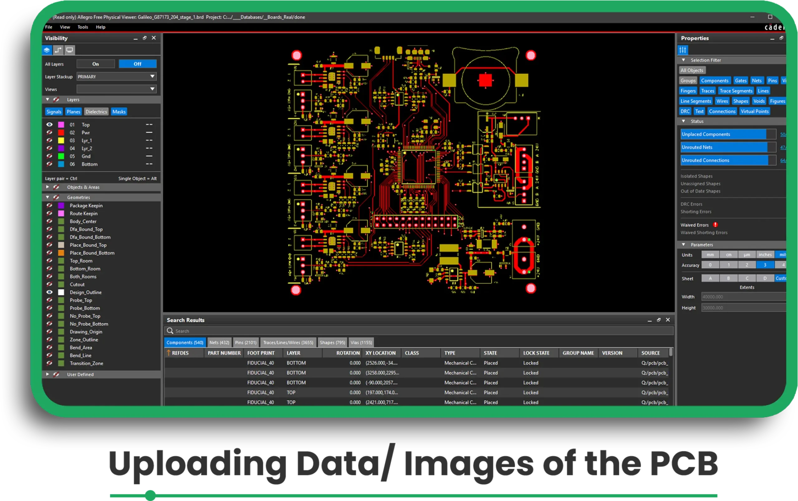
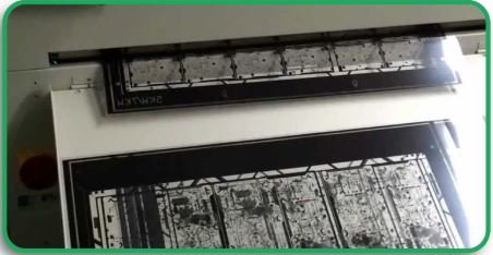
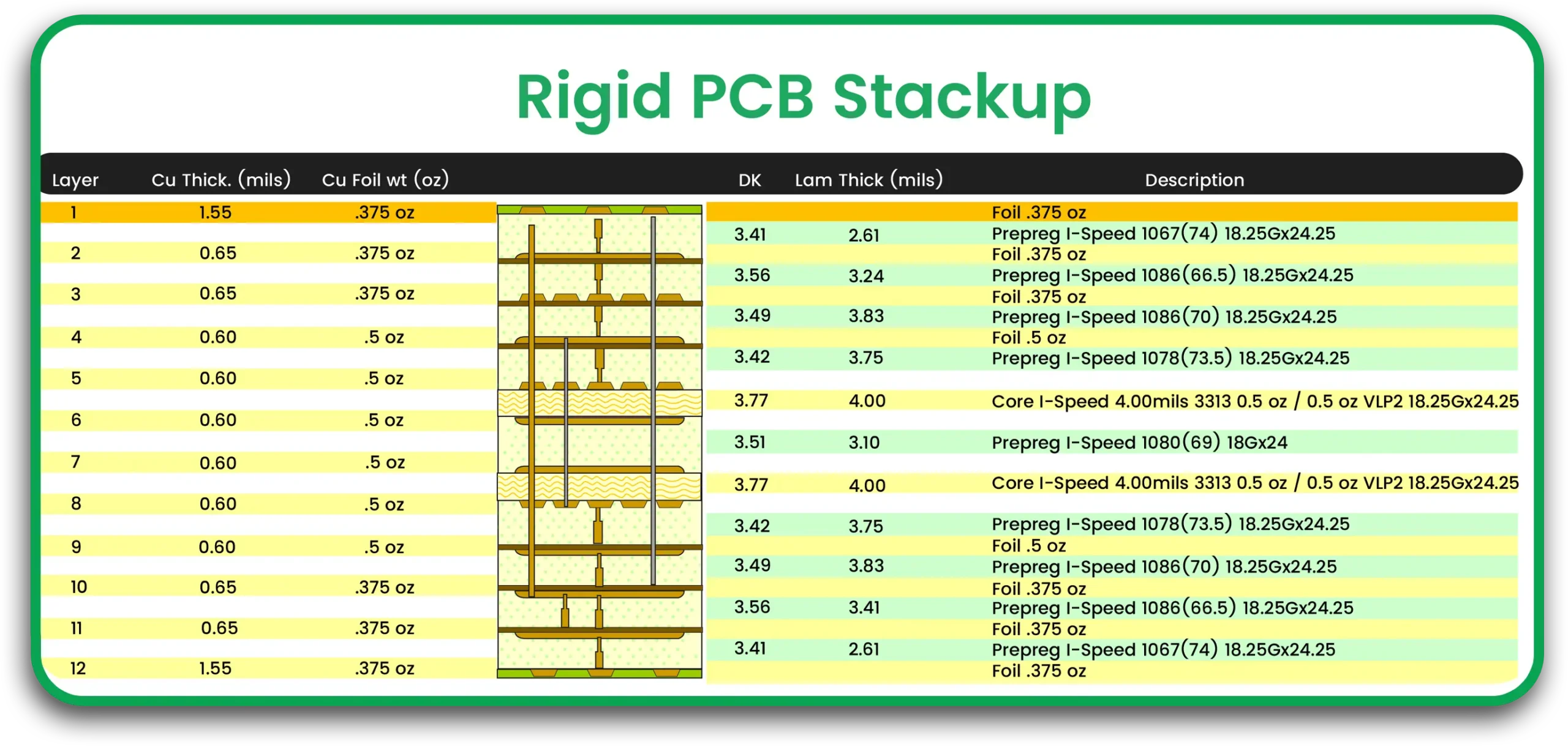
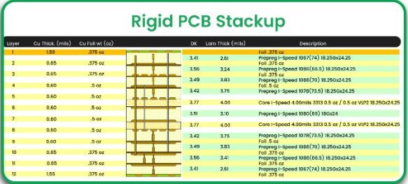
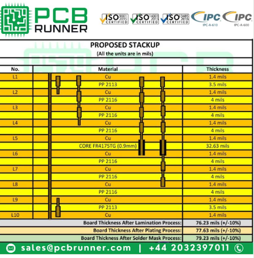
A Multilayer PCB with rigid construction consists of a stack of conductive layers separated by insulating substrates. The construction allows for more routing options for the signal within a compact space. 

These PCBs improve the connection density and functionality by integrating different layers together with more materials, such as FR-4, a fire-retardant fiberglass epoxy, for reliability and durability. 

With multiple layers, the signal integrity is significantly improved because the chance of interference and signal loss is greater over long distances. 

Key Properties of Multilayer Rigid PCBs. 

Electrical Properties: 

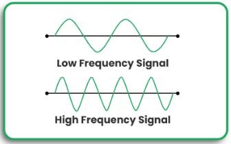
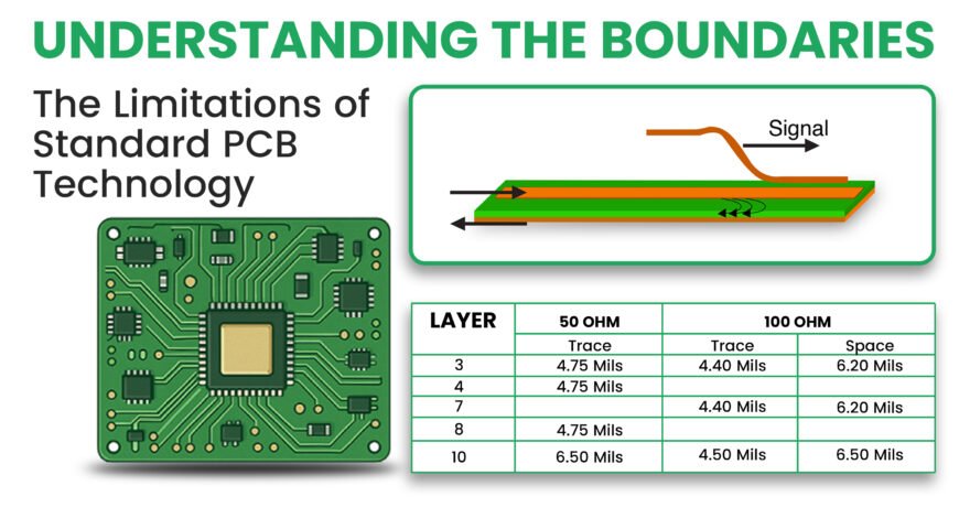
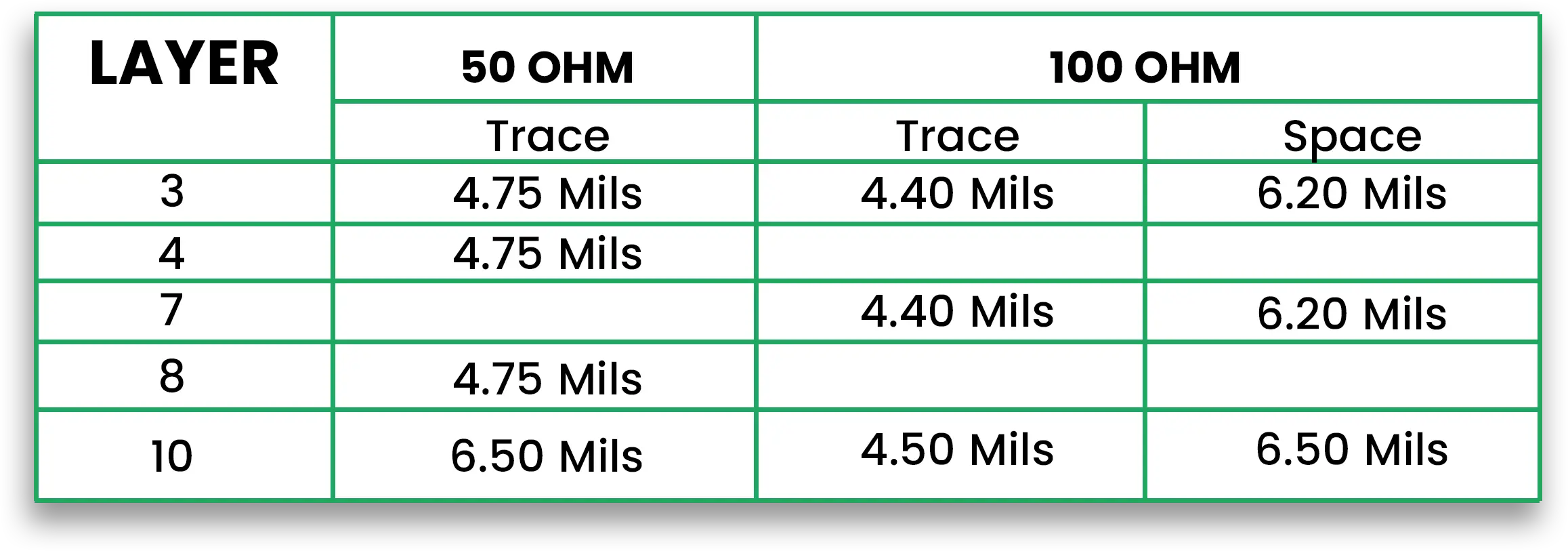
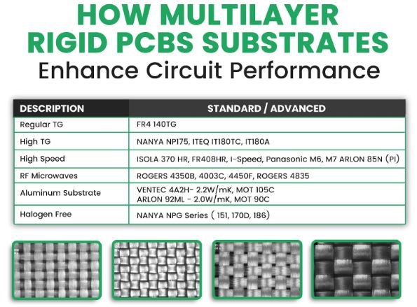
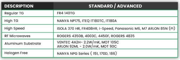
  • Dielectric Constant: It is one of the properties of signal integrity. Low dielectric constant materials such as FR-4 and others are often preferred for high-frequency applications because these materials have low dielectric constant. 
  • Dissipation Factor: It is one of the thermal properties of a low dissipation factor material, which helps minimize energy loss in the PCB material and improves the circuit’s efficiency. 

Thermal Properties: 

  • Glass Transition Temperature (Tg): The Tg value determines a material’s thermal stability. A material’s ability to withstand thermal damage is greatly dependent on its Tg value. 
  • Thermal Conductivity: It is important to manage heat in circuits with high-power components. Multilayer PCBs have better thermal management because they are designed to dissipate heat more effectively.

Mechanical Properties:

  • Peel Strength: The peel strength between copper and dielectric layers ensures that the adhesive bonds maintain structural integrity and durability during service.
  • Flexural Strength: Flexural strength ensures that multilayer PCBs endure stress or bending forces, which is very useful for portable devices and many rugged applications.

Materials

Benefits And Advantages

The electrical inclusion of multilayer rigid PCBs in electronic designs offers several benefits that improve circuit performance:

  • Improved Signal Integrity: The use of multilayer PCBs reduces the requirement of long and extensive traces, which cause signal loss and interference. This is critical in high-frequency circuits where signal integrity is a priority.
  • Better Thermal Management: With more layers to dissipate heat, multilayer PCBs can use high-power components without overheating. This is very important in devices with intense performance requirements, such as smartphones and automotive electronics.
  • Enhanced Miniaturisation: More components can be integrated into one compact board so that multilayer rigid PCBs enable smaller devices without performance degradation.

Expert Insights

The rigid flex multilayer PCB technology permits the use of fewer connectors and large harnesses for the interconnection of functional electronic systems. It increases the performance and makes it less complicated to handle packaging for high-durability space electronic systems while weighing and taking up less space for the modules. 

Here, only adhesive-free all-polyimide flexible laminates core, and no-flow glass-polyimide prepregs are utilized. A new process technology is introduced in this work to address manufacturing challenges like registration, coverlay protrusion on rigid areas, and residual copper left at the flexible and rigid junctions. 

Science has been worked out and implemented after determining the right combination of flexible, rigid, and low-flow prepreg materials. 

FAQs

Q1: What is the difference between single-layer and multilayer PCBs? 

Multilayer boards incorporate more than two conductive traces, enabling them to connect to other boards. This makes the signal stronger than on a single-layer board. 

Q2: Why is thermal management important in multilayer PCBs? 

Multilayer PCBs carry high-power components, which generate a lot of heat and require proper thermal conductivity to operate effectively without damaging the delicate components within the device.

Q3: In what ways do multilayer rigid PCBs positively improve signal integrity? 

Using multilayer PCBs helps shorten signal traces while encapsulating them inside layers to reduce signal interference and losses, which is significant in high-frequency circuit scenarios.

Q4: Do multilayer rigid PCBs have a greater budget than single-layer PCBs? 

Yes, multilayer rigid PCBs are usually more expensive because of the extra layers and construction means; however, they are far superior in outperformance and compactification.

Conclusion

Multilayer rigid PCBs are instrumental in improving circuit performance. They provide better signal integrity than single-layer PCBs, efficient thermal management, and mechanical robustness. These unique features enable their utilisation in the most advanced systems, including telecommunications, automotive, and IoT.

Take a look at our multilayer PCB solutions for increased efficiency and performance in your designs. Also, remember to subscribe to the latest updates in PCB technology and design.

PCB Assembly

From Design to Production: The PCB Assembly Process Simplified

Turning abstract designs of printed circuit boards (PCBs) into real, working products involves many tasks and requires attention to detail. This intricate process is something that both engineers and PC board manufacturers focus on to ensure seamless functionality.

PCB Runners specializes in printed circuit assembly, which has become a central activity for the company as it enables quick, dependable, and effective assembly of PCBs according to the drawing provided and functional specifications. 

We will simplify the PCB assembly process by designing the board assembly and then the case. If you are looking to make new prototypes or limited series, this is a good starting place, significantly to gain a better perspective of the steps involved. 

PCB assembly is an important aspect of consumer, medical, automotive, and industrial electronics, as it is used in key industries.  

Understanding these processes will aid those working on them in achieving high-quality production efficiently.

Key Information  

The entire process of assembly technology is captured in this diagram sequentially. Below are the steps on how it is performed: 

Step 1: Uploading Data/ Images of the PCB 

eC-smart tools such as the PCB Visualizer have enabled engineers to check their designs before the assembly phase commences. 

The company has to upload the images of the bare board for processing. 

Uploading data

Step 2: Uploading BOM and CPL Files 

The BOM (Bill of Materials) includes all component items, such as part number, description, and packaging. 

The Component Placement List (CPL) describes the location of all components on the board. 

bom

Step 3: Component Sourcing and Ordering 

An integrated system scans the BOM against the database of over 205,000 components to look for stock coverage. 

If components are not stocked, they need to be ordered from reputable suppliers through integrated APIs. 

Component Sourcing

Step 4: Front-End Component Verification 

For mounting, the correct placement, polarity, and type of package to be used against the PCB footprint are verified. 

Special requirements for mounting are determined and corrected in this phase.  

Step 5: Kitting and Component Preparation 

Items are arranged in feeders for better organisation, ensuring that they are loaded into the pick-and-place machines efficiently. 

Kitting & Component

Step 6: Solder Paste Application 

Until this phase, jetting or SMD stencil printing performs solder paste application to the PCB surface. 

A solvent paste inspection (SPI) carries out the cure check to determine the paste’s adequacy for the ensuing procedure.

Solder paste

Step 7: SMD assembly: pick & place

SMD components are positioned on the board automatically by pick-and-place machines. 

Thus, vision cameras inspect components for their sizes and angle position. 

Smd assembly

Step 8: Reflow Soldering 

The board is passed over a reflow oven, which helps melt the solder paste into a solid state, creating an inlet electrical connection to the components and PCB pads. 

Reflow Soldering

Step 9: Optical and X-Ray Inspection 

PixPect optical inspection scans the board for defects and correlates the image with properly scanned sheets. 

3D X-ray inspection can (with Nikon) detect concealed soldering connections and check the building quality of BGAs and LGAs components. 

Optical & x ray inspection

Step 10: THT Component Soldering 

Through-hole ones are assembled by means of selective soldering machines or manual soldering techniques

THT

Step 11: Final inspection and cleaning 

The final inspection should make sure that the assembled board is suitable for the design specifications. 

Before shipping, the board is cleaned, and all defects are corrected. 

Final Inspection

Benefits and Application 

Step by step understanding of the PCB assembly enables one to undertake the following actions: 

  • Enhancing Quality Control: By ensuring validation checks at many processes, the chances of committing errors are greatly minimized. 
  • Facilitate AI Methods: Integrated systems like automated component ordering and solder paste dispensing help to achieve quick turnarounds. 
  • Guarantee Component Fitting: Employing tools like PCBA Visualizer guarantees that components are placed and fit in accordance with the PCB’s design. 

By following the above guidelines, accurate, high-quality PCBs are produced with shorter lead times, making it an essential resource for PC board manufacturers seeking efficiency in production.

Expert Insights:

The following information is mentioned in the PCB Design Tutorial by David L. Jones.”

Many people start designing a PCB by placing all the components where they think they’ll fit best right away. While this approach might work for simple circuits, it’s not ideal for more complex designs with hundreds of components and multiple functional blocks. 

The main reason is that you can quickly run out of “routing space,” which is the space needed to lay down all the tracks (connections). If you fix the positions of all components first and then try to connect them, you may find yourself stuck and unable to route some connections. On the other hand, if you space the components too far apart, you may end up with a large board that wastes space and increases PCB board manufacturing costs. 

An inexperienced designer’s board often has evenly spaced components but messy tracks and vias (holes for connections) crisscrossing all over. This kind of design might work, but it’s inefficient, unattractive, and more expensive to produce. 

The best way to start is by placing all the components on the screen first. If you’re using a schematic design tool, you can import the design into your PCB program to automatically place the components. If you’re only using a PCB program, you’ll need to select components from the library and place them manually. 

Once all the components are on the screen, you can assess whether they’ll fit within the size and shape of your board. If the fit is tight, you’ll need to position the components carefully to save space and keep the routing efficient. 

If you have plenty of space, you can be more flexible with your layout. However, if the components don’t fit at all, you’ll need to revisit your design and adjust. 

FAQs 

What files do I need for PCB assembly? 

To ensure smooth printed circuit assembly, you need to upload the bare board data, BOM (Bill of Materials), and CPL (Component Placement List)

What is the purpose of solder paste inspection (SPI)? 

SPI ensures that the correct amount of solder paste is applied to the PCB pads, which is critical for proper soldering and component attachment. 

How does the pick-and-place machine work? 

The pick-and-place machine automatically picks up SMD components and places them onto the PCB, ensuring precise component placement. 

What is selective soldering? 

Selective soldering is a technique for attaching through-hole components to the PCB. It ensures precise solder joints without affecting nearby components. 

Why is X-ray inspection necessary in PCB assembly? 

X-ray inspection is essential for checking hidden solder joints, particularly for difficult-to-inspect components like BGAs (Ball Grid Arrays) and LGAs (Land Grid Arrays). 

Conclusion  

The PCB assembly process involves a series of well-coordinated steps that ensure the final product is functional and high-quality. From design verification to component sourcing and final inspection, every phase plays a vital role in producing reliable PCBs. 

By understanding this comprehensive process, both engineers and PC board manufacturers can make informed decisions that lead to faster production times and more cost-effective solutions for prototypes and small series production.

Essential Prototyping Techniques for High-Frequency PCBs

Introduction

Prior to constructing high-frequency printed circuit boards (PCBs), it is crucial to create a prototype. Such PCBs have applications in telecommunications, aerospace, and medical devices, where quality and operating efficiency are important areas of focus. Having a dependable and accurate PCB prototype helps resolve most of the potential problems before bulk production begins.

Low Frequency Signal Vs. High Frequency Signal

In this article, we explore the critical prototyping techniques used in the development of high-frequency PCBs, the impact of best practices, and innovations in design and performance, such as rigid-flex PCBs.

Essential Prototyping Techniques for High-Frequency PCBs

Here’s What You Need To Know

Concepts of Prototyping on High-Frequency PCBs

The following is what to look out for when prototyping a PCB of a high frequency:

  • Choose A Material: Opt for Rogers laminates, which are low-loss dielectrics, to reduce signal strength and impedance variations.
  • Control the Impedance: It is critical to maintain consistent impedance to avoid signals reflecting back and losing integrity.
  • Optimize Layer Stackup: The PCB design must consider the structure of layers to control EMI and lessen crosstalk.
  • Optimize Vias: Employ blind, buried, and micro vias to reduce parasitic inductance.
  • Routing Traces: To improve signals, use controlled-impedance traces with matched lengths, reduced bends, or avoided right-angle bends.
  • Thermal Management: Heat dissipation techniques should be utilized to improve high-frequency circuit stability.
  • Test and Validation: Obtaining an accurate performance read with TDR and VNA guarantees enhanced testing techniques.

High Frequency PCB

Benefits and Application

The following are the salient features of this section’s focus on prototyping techniques for high-frequency PCBs.

  • Improved Signal Integrity: Misbalanced impedance and poor routing of traces heavily distort signals and cause them to be lost.
  • Reduced Development Costs: It saves time and resources if flaws are spotted early in the design stage.
  • Enhanced Design Flexibility: Rigid-flex PCB designs increase constructional load but make the board lightweight and compact, which is helpful in fast-moving scenarios.
  • Scalability: A properly designed PCB prototype can transition effortlessly with few alterations to mass production.

By applying these techniques, engineers can create more affordable but dependable high-frequency PCB designs that satisfy the industry’s requirements.

Expert Insights

Designing embedded systems with high-frequency components involves several complex challenges, particularly when incorporating both analog and digital signals. Mixed-signal design issues, such as signal integrity, power integrity, and electromagnetic interference (EMI), are common in systems with components like WiFi, BLE, or Ethernet interfaces. \

To tackle these, board designers must focus on key aspects like stack-up design, component placement, and routing. The goal is to isolate high-frequency digital and analog signals, ensuring that they do not interfere with each other, particularly when dealing with RF functionality. 

Proper grounding and isolation of different sections within the PCB layout can minimize crosstalk and signal degradation, leading to more reliable and efficient designs. Furthermore, a high-layer count stack-up is often necessary to accommodate both high-speed digital interfaces and analog components, ensuring impedance control and power integrity.

In addition to the foundational design considerations, designers must pay close attention to the routing of high-frequency signals. Techniques such as coplanar waveguide routing and stripline routing on dedicated layers can prevent interference and ensure signal quality. It is also essential to track return paths carefully and keep RF interconnects isolated from digital components. 

Evaluating the design using advanced tools like field solvers before prototyping can help detect potential issues with signal and power integrity. These tools calculate crucial parameters such as impedance matching, network parameters, and radiated EMI, ensuring that the final design meets high-frequency performance standards. 

By addressing these challenges early in the design process, engineers can create high-performance embedded systems with seamless analog and digital integration.

Frequently Asked Questions

1. What materials work best for high-frequency PCBs?

For instance, Rogers, Isola, and Taconic laminates are all capable of providing low dielectric loss and stable performance at high frequencies.

2. What steps do I take to achieve controlled impedance on my PCB sample?

Accurate trace width calculations, the controlled impedance stack-up technique, and simulation software achieve controlled impedance.

3. Why would one opt for rigid-flex PCBs in high-frequency operations?

The design is favored for compact designs, superior signal quality, and superior resistance to harsh environments.

4. In what ways are via configurations relevant to PCB high-frequency performance?

Vias should be properly placed and selected (blind, buried, or micro vias) to reduce signal loss and other parasitic effects.

5. Is there a benefit to building a thermal prototype?

Adding thermal vias, heatsinks, and specific components can greatly help manage heat.

Conclusion

Mastering essential prototyping techniques for high-frequency PCBs is vital for achieving optimal performance and reliability. Whether you’re working on RF applications or high-speed digital circuits, paying attention to material selection, impedance control, and testing ensures a successful outcome.

Looking to enhance your PCB prototyping process? Explore our advanced solutions or contact us for expert assistance!

The Impact of Counterbore vs Countersink on PCB Performance

The Impact of Counterbore vs Countersink on PCB

When designing printed circuit boards (PCBs), it’s essential to understand how different hole configurations impact performance, including counterbore and countersink holes. Each of these types of holes has distinct characteristics that affect fastener placement, board strength, and board integrity. This blog explains when and how to use counterbore or countersink holes on PCBs.

By the end of this blog, you’ll learn how each kind of hole affects your PCB’s durability and assembly process. Whether you are an expert PCB designer or a hobbyist, understanding these differences will optimize your design. We’re also sharing tips on when to use each hole type.

Counterbore vs Countersink on PCB

Differences Between Counterbore and Countersink Holes

Feature Counterbore Holes Countersink Holes
Shape Straight cylindrical walls, flat bottom Conical, tapered shape
Function Allows fastener heads to sit flush with the PCB Enables screws to sit flush with a slanted surface
Opening Size Larger than screw diameter Tapered opening size, gradually narrowing
Shear Strength Higher shear strength due to vertical walls Lower shear strength, especially in high-load applications
Material Removal Less material removed, preserving strength Requires more material removal

Counterbore vs Countersink on PCB

When to Use Each Type

Counterbore Holes:

  • To hold heavier pieces of components in place
  • Use them in heavy-duty shear conditions like automotive and industrial systems.
  • Screw is held tighter and is not easy to unscrew.

Countersink Holes:

  • Ideal for space-saving and low-profile designs
  • Common in consumer electronics and aerospace, where aerodynamics are important
  • Suitable for aesthetic finishes

Benefits and Application

Knowing when to apply counterbore or countersink holes will directly influence the strength, aesthetic, and efficiency of your PCB designs. For high-stress applications, counterbore holes provide better screw retention and shear strength. They are ideal for industrial or heavy-duty applications.

Countersink holes are ideal if area efficiency or a smooth surface finish are important. In fact, they often dominate applications in electronics, where compactness and sleek finishing are paramount.

The right choice of hole type will, therefore, help improve the mechanical stability and aesthetics of your PCB and achieve the desired performance in its application.

Expert Insight 

Integrating countersink and counterbore holes into PCB design is essential for achieving a seamless mechanical fit within an enclosure while maintaining structural integrity. Countersinking allows screws to sit flush with the board surface, which is particularly beneficial in compact assemblies where space is limited, and a smooth profile is required. On the other hand, counterbore holes accommodate socket-head or cap screws by creating a recessed cavity, offering improved load distribution and enhanced mechanical stability. Altium Designer provides robust tools to define these hole types with precision, allowing designers to specify critical parameters such as mounting hole diameter, countersink angle, and counterbore depth. This level of detail ensures compatibility with chosen fasteners and facilitates accurate manufacturing outputs.”

“To maximize the effectiveness of countersink and counterbore features in PCB layouts, designers must consider factors such as the type of fasteners, enclosure constraints, and fabrication capabilities. Properly defining hole dimensions and tolerances in the design phase minimizes assembly issues and improves product reliability. Altium Designer’s integration with fabrication outputs, such as NC Drill Files and IPC-2581, ensures that counterholes are accurately translated to manufacturing. Additionally, features like the Hole Size Editor and Draftsman tool provide clear documentation and visualization of counterhole specifications, streamlining communication with manufacturers. By leveraging these capabilities, engineers can enhance both the functionality and manufacturability of their PCB designs.”

FAQs

Q: What is the advantage of counterbore and countersink?

A: Counterbore holes are more recommended for applications with heavy burdens since they are more sheared and poor in maintaining screws, so the bolts once tend to be unfixed easily. On the other hand, countersinks are more designed for flush with a tapered edge, which, in turn, is sought out by Small or aesthetic designs.

Q: What is a countersink in a PCB?

A: A countersink in PCB is defined as a hole that has a wider cone shape and allows screws or other mechanisms to fit the surface behind it. This integration goes for a smooth finish, aiding the visual appearance, and is particularly useful in designs that require a low height.

Q: What is the difference between countersinking and counterboring SDI?

A: Countersinking creates a conical hole while counterboring entails creating a cylindrical hole with a flat tip. Thus, there are differences between holes and their intended functionalities—counterbore gives the highest shear strength, but it is only for countersinks if it aims at a smoother flush finish.

Q: What is the disadvantage of countersink?

A: Countersinks remove more material than counterbores do, making the PCB weaker. Additionally, countersinks provide less shear strength and do not suit high-load or high-stress applications well.

Q: What is the advantage of countersinking?

A: The most significant advantage of countersinking is its ability to create a smooth, flush surface for screws and fasteners to be inserted, which would be applicable for applications in which aesthetics and compact design are crucial.

Q: When to apply counterbore?

A: Apply counterbore holes whenever higher shear strength, secure fastener retention, and a smooth, flush screw-and-washer fit are needed. This is especially true in heavy-duty or industrial applications.

Mastering the Process: How to Make a PCB BOM

How to Make a PCB BOM

A good plan is one of the prerequisites for starting any project. In the case of PCB (Printed Circuit Board), one of the prerequisites is to draft a Bill of Materials as detailed as possible. In addition, a BOM will list all the components’ details such as manufacturing part number, availability, date code, package size & types, electrical description, and most importantly pricing. For PCB design engineers and product manufacturing executives, it gives them the confidence to commence production at minimal, if not zero, cost overruns.

In this blog, you’ll learn the crucial elements of a PCB Components part list BOM, how it helps in the assembly process, and how to best utilize the PCB design software for the optimization of PCB design. In any case, whether you are a beginner or an advanced PCB designer. It is essential to understand the BOM, as it saves time, eliminates mistakes, and reduces production costs.

How to make PCB BOM

Key Information You Need to Know About PCB BOM

When preparing the BOM for PCB design, the components listed below should be incorporated:

  • Item Identifier: It is an index number that is assigned to each component in an index.
  • Quantity Per Board: This variant shows the number of units needed for every component on a single PCB.
  • Manufacturer Part Number (MPN): Used to ensure the proper part number is used to assemble a product.
  • Reference Designator: Enables easy identification of various parts by connecting them to positions on the PCB layout. For example: R1, C3
  • Do Not Install (DNI)/Do Not Populate (DNP): Used to mark out parts not required to be assembled.
  • Footprint/Package Type: Provides a verbal explanation of the physical size and shape of the various components.
  • Component Description: This is written to describe the detailed specifications of each of the parts.
  • Supplier and Supplier Part Number (optional): Aids in finding the components.
  • Value (optional): These include electronic details such as resistance or capacitance.
  • Lifecycle Status: This tells if the component is in production, semiconductors are not being produced, or they are going out of production soon.
  • Alternate Parts (optional): Substitute parts in case of stock shortages.

Bill of Materials

Using printed circuit board design software like Altium Designer or KiCad simplifies the process by automatically generating BOMs with these fields.

Benefits and Applications of BOM

A well-prepared BOM serves several important purposes:

All Components Under One Roof

A BOM clears up all components and sets quantities and their designations for ease of workflow. In the case of PCB circuit board manufacturers, BOM addresses the issue of production stoppage due to component unavailability and addresses chaos.

Cost Estimation

Estimation of accurate creation of BOMs assists in the creation of cost estimates in the course of preparing for production. By deductively analyzing this particular BOM, designers alter the original designs to fit given limits. In conjunction with that, BOM tools in PCB design compare vendor costs, stock availability, and even real-time pricing to vendors to aid significantly in procuring the right components speedily.

Smoother Communication

A BOM bridges gaps between designers, manufacturers, and suppliers, improving communication. When it is their turn to act in the process, any party can have all the exact required information, eliminating waiting times.

How to Create a Bill of Materials

Traditionally, BOMs were created manually using spreadsheets, but this process is time-consuming and prone to errors. Today, printed circuit board design software like Altium Designer, Allegro PCB Editor, and KiCad automates BOM generation. Here’s how it works:

  1. Design the Schematic: Draw the PCB schematic using the ECAD tool.
    Schematics Diagram

  2. Component Libraries: Select parts from built-in libraries that include manufacturer details and specifications.
  3. Automatic BOM Generation: The software compiles a detailed BOM from the schematic.
  4. Cost and Stock Analysis: BOM tools check for component availability, lifecycle status, and cost comparisons.

These steps ensure a more accurate, efficient, and up-to-date BOM.

Expert Insights

Effective PCB BOM (Bill of Materials) management is critical to ensuring a smooth production process, cost efficiency, and long-term product reliability. A well-structured BOM serves as the backbone of the entire supply chain, providing a detailed list of components, part numbers, quantities, and sourcing information. By maintaining an accurate and up-to-date BOM, manufacturers can mitigate risks related to component obsolescence, supplier shortages, and unexpected cost fluctuations. Moreover, a comprehensive BOM helps streamline communication between design, procurement, and production teams, ensuring that everyone works with a single source of truth throughout the product lifecycle.”

“To optimize PCB BOM management, it’s essential to implement best practices such as using standardized naming conventions, leveraging automated BOM management tools, and conducting regular reviews to address potential supply chain disruptions. Collaboration with trusted suppliers and incorporating alternative component options can further enhance resilience against market uncertainties. Additionally, ensuring thorough documentation of part specifications and lifecycle status aids in reducing production errors and costly redesigns. Ultimately, a proactive approach to BOM management not only enhances operational efficiency but also contributes to a more agile and responsive product development process.”

Frequently Asked Questions

Why is a BOM important for PCB manufacturing?

A BOM (Bill of material) is most important to ensure that all required components are listed, preventing missing parts and reducing production delays.

What are the must-have fields in a BOM?

Essential fields include item number, quantity, MPN, reference designator, footprint, Alternative package part number and component description.

Can I automate BOM creation?

Yes, most printed circuit board design software like Altium Designer and KiCad can generate BOMs automatically from schematics.

How does a BOM help with cost estimation?

BOM tools analyze vendor prices, bulk discounts, and alternative components to optimize sourcing and reduce costs.

What happens if a component in the BOM becomes obsolete?

Including lifecycle status and alternate parts in the BOM helps mitigate risks related to component obsolescence.

Conclusion

The BOM is the key to efficient and error-free PCB production. Designers must include all necessary details and keep them up-to-date so that manufacturing can be streamlined, costs reduced, and production delays avoided.

Don’t miss out on our updates by PCB Runners to keep you informed about PCB designing and industry information.

Picture Punch Technology: The Next Step in Custom PCB Design

Picture Punch Technology

Over the last few decades, there has been significant growth in the functionality and application of PCBs, especially with advancements like High Density Interconnect (HDI) technology that enhances performance and enables compact designs. They are utilized not only as an effective branding tool but also to enhance a product’s overall appearance significantly.

With the introduction of Picture Punch Technology by PCB Runner, PCB design has changed completely. The ability to print photo images onto Custom Printed Circuit Board gives a unique appeal while ensuring full functionality and has transformed the aesthetic value of product branding.

In this article, you will find how PCB punch technology enhances the PCB design without significantly hindering performance. You will also learn how modern electronics have adapted to the changing world of personalized designs.

Picture Punch Technology

Key Information You need

Below are some capabilities of PCB punch technology that you may find interesting:

  • Personalisation Options: Logos, graphics, and any other art can be engraved into the surface of the PCB without disturbing its functionality.
  • Easy-to-Use Tool: Easy-to-Use Tool: Upload any JPEG or PNG image, configure your preferences, and allow the system to do the magic, making it compatible with advanced PCB designs such as those using High Density Interconnect.
  • Use Cases:
    – Front Panels
    – Keyboards
    – Transparent Casing for Electronics
    – Pre – Soldered PCB Modules
    – Educational / Consumer Electronics
    – Social Impact Technologies

Benefits of PCB punch technology:

  • Enhanced Visual Appeal: Custom Printed Circuit Board are made extraordinary with an added layer of personalization.
  • Effective Branding: These brutalized PCBs are the best choice for corporates who desire a unique brand identity.
  • Effortless Way: The PCB’s aesthetics can be altered without affecting its electrical function.

Benefits and Application

By integrating PCB punch technology into your design workflow, you open the door to a variety of practical benefits:

  • Distinctive Branding: Stand out with custom graphics that resonate with consumers and partners alike.
  • Increased Marketability: A visually unique Custom Printed Circuit Board can be a significant selling point in crowded tech markets.
  • Enhanced User Experience: Your product’s PCB becomes part of the design, offering a seamless aesthetic experience for users.

Picture Punch Technology

This technology allows for simpler product differentiation, and when combined with High Density Interconnect designs, it offers enhanced functionality while maintaining aesthetic appeal. This is especially crucial in industries where visual and technical innovation can lead to stronger customer engagement and higher sales.

Frequently Asked Questions

What is PCB punch technology?

This is a function that enables you to use images or logos over the surface of the PCB.

How does PCB punch technology function?

Simply upload your image, which can be in JPEG or PNG format, and select between black or white solder mask colour or gold. The system will adjust the image to fit seamlessly into the PCB design.

What applications benefit the most from PCB punch technology?

This works best in child products, transparent casings, front panels where the electronics can be shown, and other uses.

Is there any PCB design that PCB punch technology will not work on?

No, PCB Picture works with all types of circuitry boards. Its modes of beauty and application give PCB punch technology freedom of use in areas where it appeals to the user.

Is the picture that has been incorporated on the PCB long-lasting?

Certainly, the images used with PCB punch technology are resilient and do not alter how the PCB operates.

Conclusion

There is a paradigm shift in how designers view PCB creation, such as the ability to customize the design without compromise courtesy of the PCB punch technology function.

The way graphic images are integrated into the PCBs allows for better product appeal and strong brand identity, which dramatically increases competition in the market.

Whether you need professional PCB production service providers in the UK and Europe, consumer electronics, educational purposes, or high-tech devices, combining PCB punch technology with High Density Interconnect designs can redefine the future of customized circuit boards.

Standard PCB Technology

Understanding the Boundaries: The Limitations of Standard PCB Technology

The Limitations of Standard PCB Technology

Printed circuit boards, or PCBs, are essential to the modern electronics industry because they enable high-density circuit and component integration. Despite the tremendous advancements in recent decades, PCB technology still has drawbacks.

Designers and engineers must identify these constraints in order to guarantee that they will not incur any costs during the manufacturing assembly of the product.

In this blog, we will discuss the constraints of standard PCB technology related to size, materials, performance, and manufacturing capability, including how HDI PCB manufacturing can help overcome some of these challenges. Whether you are a beginner or have experience, being aware of these limitations helps you make informed decisions during the PCB design process.

Common Limitations of Standard PCB Technology

As much advancement PCB designs and models have made over the years, they are still limited by various specific issues that were mentioned earlier that designers must not ignore.

Thickness and Dimensions of PCB Models

  • Board Dimensions: As PCBs become smaller and more compact, it becomes challenging to fit all components into a tight space without compromising functionality. This often leads to issues with component spacing and routing, particularly with HDI PCB designs.
  • Board Thickness: PCBs are manufactured with a specific thickness in mind, and increasing the thickness beyond the standard can affect the flexibility, weight, and cost of manufacturing.

Material Limitations

  • Limited Material Choices: People often use FR4 (fiberglass epoxy) to fabricate PCBs, and while that is fine and dandy, it is not the most optimal option for high-load performance requirements that have very stringent criteria, such as responding quickly to high frequency or being heat resistant.
  • Thermal Management: Super-thin standard PCB models do a poor job regulating temperature. If they are not actively managed, overheating becomes the norm, especially with high-power components. Even within the lower ranges, one can only imagine the capacity potential.

hdi pcb stack up

Signal Integrity and High-Speed Performance

  • Signal Interference: As components on a PCB get smaller and packed tighter together, signal interference becomes an increasing factor to consider. High levels of crosstalk and EMI can undermine the quality of the signal in high-frequency designs.
  • Impedance Control: Traditional PCB layouts are not very good at controlling the impedance on one or several critical high-speed transmissions. Being off in terms of impedance creates a reflection in the signal and, subsequently, the loss of the signal or its distortion.

chart

Manufacturing Constraints

  • Resolution Limits: The finer the trace width and the component pads, the harder it is to make a PCB. Conventional manufacturing tools may not be able to provide the necessary precision for HDI PCB manufacturing and microelectronic PCBs.
  • Via Limitations: Some of the restrictions imposed by standard PCBs on the sizes of vias and their locations may impact the routing of signals and power distribution, especially in multi-layer PCBs.

Component Density and Routing

  • Routing Complexity: As additional components and layers increase, the HDI PCB design becomes more complex, and routing becomes more challenging as well. The interconnection of components can require multiple layers of routing, which adds to the board’s cost and complexity.
  • Component Size: Size Reduction is a popular trend in electronics. However, standard PCB technology usually does not accommodate the very tiny components needed in gadgets such as phones or all sorts of wearables.

Benefits and Application

These restrictions sound limiting, especially for design. However, grasping these restrictions helps you make better choices during the design stages.

Becoming aware of possible risks in the early stages helps one take measures to tackle them.

For example, the designer can use an alternate set of materials, make the gap between the components more significant, or investigate better technologies such as HDI PCB manufacturing.

By accepting these limitations, designers can improve their layouts, enhance manufacturability, and reduce the chances of failure.

Expert Opinion

Expert Insight by NASA: Limitations of PCBs

Printed Circuit Boards (PCBs) are crucial in modern electronics, but the failure to address their limitations may have severe implications. Failure in PCB design or manufacturing can result in a series of problems for manufacturers and end-users. Manufacturers will experience a delay in the time-to-market of their products, increased warranty costs, and reputational damage. Such failures can discourage customers from buying, decrease market share, and raise liability claims based on damages from faulty products.

For end-users, PCB failures often translate into personal injury risks, mission-critical operation losses, and costly repairs or replacements. Beyond direct costs, such failures can result in indirect financial burdens, such as increased insurance premiums, reputational harm, and a reduced competitive edge in the market.

These limitations highlight the importance of precise PCB design, rigorous testing, and adherence to quality standards to ensure reliability and mitigate potential failures.

Frequently Asked Questions

Q: What is the most critical drawback of utilizing FR4 in the construction of high-frequency PCBs?

A: High frequency and signal integrity retain a direct relationship, so an FR4 would be inappropriate due to its dielectric constant and loss tangent, which are relatively higher than what is deemed ideal.

Q: What role does the thickness of a PCB play in the optimal functioning of a device?

A: Increasing the thickness of the PCB can have multiple drawbacks. While it can reduce the overall board flex, it will also increase the weight, temperature, and rigidity, which may affect heat dissipation.

Q: Is it possible to enhance or retain a circuit performance while reducing the area occupied by a PCB?

A: Yes, but there are plenty of factors that must be considered. Small PCBs do require density components with smaller traces; however, some innovative methods can still be employed to retain the circuit’s signal integrity.

Conclusion

Understanding the limits of standard PCB technology is critical for achieving cost-effective and trustworthy designs. Awareness of these limitations should be established at the beginning of the design so that decisions can be made to increase the PCB’s efficiency.

In-Circuit Testing vs Functional Testing: Which One Is More Effective?

In-Circuit Testing vs Functional Testing

Once a PCB fabrication & PCB assembly is completed, quality and reliability testing are performed to ensure the final product’s functionality. Numerous methods are used for testing, two of the most popular being In-Circuit Testing and Functional Testing.
Though both of these testing methods are used to achieve quality control, their results, outputs, and mechanisms are different.

Understanding the differences between these methods allows manufacturers to select which one better fits their requirements. In this blog, we will discuss the merits and demerits of ICT and FCT and what scenarios they can be used for.

This blog will provide insights into the effects each of these testing methods has on the final PCB prototype and assembly’s performance and reliability.
From an experienced PCB engineer to a novice in the field, everyone will be able to comprehend which testing mechanism meets their needs and how reducing testing costs will increase product quality.

In-Circuit Testing vs Functional Testing
In-Circuit Testing (ICT):

Purpose: The ICT is used to look for breakages such as open connections, shorts, misaligned components, and incorrect component values on the PCB during circuit and component testing.

How it works: During the ICT, a custom “bed of nails” fixture is utilized to test various parameters of each board component by applying electrical signals to it and measuring its resistance and capacitance.

Beds of Nails Testing

Pros:

– Manufacturing defects can be located quickly and accurately

– The chance of assembling the parts on non-functional / X-Outs circuits gets low.

– It is suitable for mass production.

Cons

The need for unique test fixtures implies that these tests come with a significant initial cost.

It does not examine the PCB in actual operating conditions, which limits its scope.

Functional Testing (FCT):

Purpose: It functions by testing the PCB as a part of the final product in a box build assembly but in controlled alternative conditions. 

How Does It Work: A test fixture is applied that shows output readings, such as the assembly’s temperature, voltage, or frequency, allowing it to serve its purpose and also could be an indication on testing equipment with green/red leads.

Functional TestingPros:

-It allows do attempt of the final product to a detailed examination of the operative capacity and operating nature.

-The product is able to function in real-life conditions while being assembled, supporting the desired output considered by product designers.

Cons:

-Requires custom testing equipment to support high-end technology, which can be difficult to procure.

-It is a bit more costly due to the complexity of dealing with and ordering custom test fixtures, but the savings in time make it worth the cost.

Benefits and Application

Using Either ICT or FCT along with the correct testing method has plenty of benefits. Utilization of the correct testing strategy has its share of benefits. Using one or the other has some abnormalities on the testing side that should not hamper overall operation.  

In-circuit testing (ICT)

It aids in the detection of manufacturing anomalies like shorts or open connections. Therefore, it reduces the chances of the final product having flaws by enabling each element to be assembled appropriately. It is most beneficial in mass production when speed and accuracy in servicing are major requirements or concerns.

Functional Testing (FCT)

It is highly valuable in conditions where the board is of great use, and diagnostic functionalities are critical, such as consumer electronics, automotive testing, and medical emitters. It inspects whether the complete system is functional and ready to be used by checking whether all the parameters regarding a working system were met.

Expert Insights

The integration of In-Circuit Testing (ICT) and Functional Testing (FCT) has evolved to meet the demands of modern PCB assembly”. Modular circuit designers offer flexibility and scalability by allowing subsystems like the ICT module and the FCT module to be upgraded or replaced independently. This is useful for adapting to different testing requirements or technological advancements.

On the other hand, unified testing platforms consolidate both ICT and FCT capabilities into a single hardware/software framework. This approach simplifies configuration and operation, making it easier to manage the testing process. However, it may limit flexibility and expandability compared to modular architectures.

A hybrid approach combines the best of both worlds, offering both the flexibility of modular designs and the integration of unified systems. This balance ensures both scalability and streamlined testing operations.

Frequently Asked Questions

Which is better, functional testing or performance testing?

Both are important and better. Performance testing measures a PCB’s specific electrical characteristics which is also called as E-Testing (after fabrication is done), while functional testing evaluates its overall performance under real-world conditions which also called as Bootup Testing (after pcb assembly) Functional testing is usually more comprehensive and useful for confirming a product’s functionality.

What are the advantages of using in-circuit testing?

In circuit test is also known as ICT / NET List testing. The accuracy and speed of in-circuit testing can also detect assembly or manufacturing errors, such as shorts, open connections, or missing nets or stubs. The core advantage of running ICT test before PCB Manufacturing is that it allows to give surety to a manufacturer that there are no Nets shorting with guaranteed to be correctly routed and assembled without the application of power shorts so that the components will not be damaged.

What is a functional circuit test?

FCT Functional Test is used to check the electric parameters and specifications of the device. It checks the electrical parameters and specifications of a PCB assembly by functioning the device in a normal environment where the assembly is expected to work.

What are the 7 types of PCB testing methods?

  • In-Circuit Testing (ICT)
  • Functional Testing (FCT)
  • Flying Probe Testing
  • Automated Optical Inspection (AOI)
  • X-Ray Inspection
  • Boundary Scan Testing
  • Burn-In Testing

Conclusion

Both In-Circuit Testing and Functional Testing complement each other in terms of ensuring the quality and reliability of PCB assemblies. While ICT is suitable only for identifying defects, FCT, on the other hand, assesses the overall functional capability of a PCB when placed in real-life scenarios.

This is important because if manufacturers can effectively utilize all the pros and cons of each method, they will ultimately reduce the cost of the testing while improving the quality of the product.

Why Rigid HDI PCB Substrates Are Essential for IoT Devices

Why IoT Devices Rely on Rigid HDI PCB Substrates

The Internet of Things (IoT) is improving at a rapid pace, and there is a need for faster, more compact, and reliable products. The need for per unit surface area has risen drastically, which sets the goal for Rigid HDI (high-density interconnect) PCBs. 

These new PCBs make it easier for designers to fit more functionality into a smaller space, which is more important than ever for constrained and cluttered IoT applications. With the increase of connected devices, it is important for all individuals targeted at IoT development to understand the relevance of Rigid HDI substrates.

In this blog, we will discuss HDI PCB fabrication, the performance and miniaturization of Rigid HDI PCBs enabling IoT devices, their advantages, and the reasons they are essential for modern electronics.

Why Rigid HDI PCB Substrates Are Essential for IoT Devices

What Are Rigid HDI PCBs?

High Density Interconnect (HDI) PCBs offer greater circuit density in a smaller area due to the inclusion of thin traces, small pads, and miniaturized vias.

These kinds of PCBs are designed to transfer signals quickly. They feature advanced micro vias, buried vias, and blind vias to achieve compact and complex designs.

Rigid HDI PCBs are ideal for IoT devices as they provide advanced features. Their higher I/O counts, smaller size, and better performance make them suitable for multilayer boards.
In IoT, the Benefits of Rigid HDI PCBs are:

  • Improved signal: Smaller vias greatly improved performance in high-speed IoT applications by reducing signal degradation.
  • Miniaturization: HDI boards allow smaller electronic devices to be designed with a higher level of functionality. This is perfect for portable devices, wearable goggles, and many other devices where space is constrained.
  • Cost Efficiency: The rigid HDI PCBs housing multiple components in a single unit allow for a drastic reduction in the number of components.
  • Increased Reliability: Reducing the number of components and making the electrical connections stronger increases the performance and durability of IoT devices.

Rigid PCB Stackup

Application and benefits:

Including HDI PCB prototypes in your IoT designs helps achieve better signal integrity, compact form factors, and enhanced connectivity. Smart home systems, healthcare sensors, and wearable gadgets are all IoT devices that rely on increasing their overall performance while reducing their size.

Fitting several devices and their connections into one small board can greatly reduce costs and improve the time taken to manufacture new IoT products.

Expert Insights

Rigid HDI (High-Density Interconnect) PCBs are essential for IoT devices, offering superior performance in both compactness and functionality. As IoT technology demands smaller, more powerful, and cost-effective devices, rigid HDI PCBs provide the high-density interconnections needed to support advanced features in space-constrained applications. 

These substrates are crucial for ensuring efficient signal integrity and thermal management, key aspects for IoT systems operating in diverse and often harsh environments. Additionally, the use of rigid HDI allows for the integration of fine-pitch components and complex routing, which are indispensable for modern, miniaturized IoT devices.

Moreover, rigid HDI PCBs enhance the durability and longevity of IoT devices by providing robust mechanical strength and moisture resistance. These boards excel in high-performance IoT applications, such as smart grids, autonomous vehicles, and medical devices, where reliability is non-negotiable. Their ability to withstand thermal cycling and environmental stress makes them ideal for IoT solutions that require long-term performance under varying conditions.

The combination of compact design, high thermal stability, and efficient manufacturing processes makes rigid HDI PCBs the go-to choice for cutting-edge IoT devices, enabling both functionality and sustainability in an increasingly connected world.

FAQs

Q1: What are the differences between HDI PCBs and other PCBs?

HDI PCBs have unique designs, offering greater electrical performance and higher-density interconnections compared to traditional PCBs, which have less efficient traces and vias.

Q2: Is it possible to use Rigid HDI PCBs for all IoT devices?

There is no question that Rigid HDI PCBs are flexible and can be fitted to various types of IoT applications, including wearable devices, smart home gadgets, and even industrial sensors.

Q3: How economical is rigid HDI PCB fabrication at mass scales?

Although HDI Rigid PCBs entail higher initial production costs than conventional methods, they become economical once multiple circuit boards are combined into one compact device, decreasing the number of additional parts needed.

Q4: How can Rigid HDI PCB enhance the efficiency of the signals?

Because of their distinct characteristics, advanced HDI PCB construction techniques such as microvias and blind vias can truly benefit signal integrity in high-frequency settings. Microvias mitigate signal loss, and blind vias significantly reduce interference and crosstalk.

Conclusion 

The market is trending towards low-cost, highly functional, fully integrated IoT devices. To stay competitive, adopting Rigid HDI PCBs will help improve your IoT product design, increase reliability, and improve the time to market.


Rigid HDI PCB substrates

Over the past few years, printed circuit board technology has advanced dramatically. It demands goods that are both faster and more compact. HDI boards are considerably smaller now. They have tiny pads, copper traces, ultra-fine vias, and gaps.

HDI-printed circuit boards have significantly higher wiring density per unit than traditional printed circuit boards. HDI PCBs are typically defined as printed circuit boards with micro vias, blind vias, buried vias, high signal functionality, and built-up laminations.

Thus, high-density layouts have denser wiring, resulting in lighter weight, fewer layers, and more condensed PCBs. Instead of using multiple PCBs in a device, a single HDI board is adequate to house the functionality of the prior boards.

  • Finer lines and spaces < 100 um / 0.01 mm
  • Smaller vias<150 um and capture pads <400 um / 0.40mm
  • Higher connection pad density > 20 pads/cm2
  • 120-160 average pins per square inch

Rigid HDI PCB substrates

Benefits of Rigid HDI PCB Substrates:

  • Better electrical performance and signal integrity
  • Lower noise and crosstalk, and lower EMI/RFI
  • Smaller size and weight
  • Cost optimization
  • Reduced design time
  • More reliable designs
  • Complex and dense devices
  • Compact PCBs

When designing an HDI PCB board, it is critical to keep important manufacturing and design challenges in mind. There are a few of the most commonly reported difficulties:

  • More connections are required to finish the board.
  • You must design smaller parts in a much narrower space.
  • There are relatively few workplace areas.
  • There is a restricted board workstation area.
  • There are more parts on each side of the PCB layer.


Features PCB Runner’s Specialty
Number of layers 4–22 layers standard, 30 layers advanced
Technology highlights Multilayer boards feature a higher connection pad density than normal boards, with thinner spaces, smaller via holes, and capture pads, allowing micro vias to only penetrate specific layers and even be inserted in surface pads.
HDI builds 1+N+1, 2+N+2, 3+N+3,4+N+4, any layer or ELIC, Ultra HDI in R&D
Materials FR4 standard, FR4 high performance, halogen-free FR4, Roger
Copper weights  18μm – 70μm
Minimum track and gap 0.075mm / 0.075mm
PCB thickness 0.40mm–3.20mm
Maximum dimensions 610mm x 450mm; dependent upon the laser drilling machine
Surface finishes 0.10mm standard, 0.075mm advanced
Minimum mechanical drill 0.15mm
Minimum laser drill 0.10mm standard, 0.075mm advanced


Types of Rigid HDI PCB Substrates:

A via is a tiny conductive hole that connects multiple layers of a PCB with a high density of interconnectivity. It provides signs so that one can pass across them with ease. Four different kinds of through holes penetrate into an HDI PCB, all of which are subject to PCB operations.
These are the following:

Blind Vias

To link the center layer of a multi-layered HDI PCB to the periphery, a drill or laser is used to punch the hole. The reason this hole is called the blind via is because it is only visible from one side of the PCB board. But keep in mind that this kind of hole is expensive and difficult.

Buried-vias

The multiplayer HDI PCB’s two inner layers are connected via the buried vias. It gets its name since it is always located on the internal surface of the printed electronics board and is invisible from the outside. A different drill file is needed for this via since it is also a plated hole. A buried passage has an even number of layers, such as 2, 4, 6, 8, and so forth.

Micro-vias 

The micro vias, as their name suggests, are the smallest form, measuring less than 150 microns in diameter. A laser is also used to puncture it. These are among the most common kinds of vias used in HDI PCBs to connect one layer to the one next to it. In addition, its diameter is much smaller than that of mechanically bored vias, such as the through-hole. They are able to manufacture boards for electronics with more complex designs that are denser because of their size and ability to connect layers.

Via-holes

A drill or laser is used to drill this hole from top to bottom across the PCB. It facilitates the connection of the multi-layer PCB’s layers. Not only are they easy to build, but they are also among the most cost-effective options. To make them more inclusive, they have been separated into non-plated-through and plated-through holes.

Compared to microvias and through-hole vias, HDI technology offers a number of benefits, which include:

  • Improved consistency: Compared to traditional PCBs, HDI PCBs are more trustworthy and less prone to damage since they contain fewer features and more densely packed interconnections.
  • Improved performance: HDI PCBs are compatible for faster signal transfer, feature a greater number of connections, and provide improved performance for electrical devices.
  • Higher densities of interconnections are supported by HDI technology, meaning that more superior connections can be constructed in a smaller space. It is essential for producing smaller and more complex PCBs.

HDI PCBs Structures:

HDI PCB (1+N+1): Simplest HDI

  • One “build-up” of high-density connector layers makes up this HDI PCB structure, making it appropriate for BGAs with fewer I/O counts.
    • It features great mounting stability and dependability, fine lines, registration technologies with a 0.4 mm ball pitch, microvia, and the potential for copper filled via.
  • Applications: GPS, memory card, MP3 player, and cell phone.

HDI PCB (2+N+2): Moderate Complex HDI

  • Two or more “build-up” of high-density connection layers make up the HDI PCB structure; microvias on various levels can be stacked or staggered; Copper-filled layered micro via structures are frequently found in difficult designs with demanding specifications for high-performance signal transmission. 
  • These can be utilized to boost routing density in a complex design while keeping a thin final board thickness; they are appropriate for the BGA with smaller ball pitch and greater I/O counts.
  • Applications include game consoles, PDAs, cell phones, and portable video recorders.

ELIC (Every Layer Interconnection): Most Complex HDI

    • All of the layers in this high-density interconnection (HDI) PCB topology enable free connectivity of conductors on any layer via copper-filled stacking microvia structures. 
    • This produces improved electrical characteristics and offers a dependable connectivity solution for extremely complicated big pin-count gadgets, such as CPU and GPU processors used in portable and mobile devices. 
  • Applications include memory cards, MP3, GPS, cell phones, ultra-mobile PCs, and compact computers.

Why choose our Turnkey Manufacturing?

PCB Runner offers turnkey solutions which include custom design layout, fabrication, components procurement & assembly labor, for all industries. Our expert design layout team efforts help the end R&D engineers/ Buyers/ Purchasers to reduce their time by going back & forth to design PCBs based on manufacturing capabilities & running DFM & DFA twice. 

You are welcome to submit your design files to our email at sales@pcbrunner.com or engineering@pcbrunner.com