PCB Layout Design for Electromagnetic Compatibility: A Guide for Optimal Performance

Every electronics industry professional today understands the requirement of a reliable PCB design that meets EMC standards. To keep up with the power and compactness of new devices one must keep in mind the risk of electromagnetic interference (EMI) that can truncate the overall performance. 

Thus, every PCB manufacturer or designer must tackle the challenges of an interference-free operation while designing the PCB layout, which is critical to a PCB design achieving EMC standards.

This blog will discuss the key principles of electromagnetic compatibility and offer tips to manage EMI and overall performance. It is crafted not only for seasoned PCB manufacturers but also for designers aiming to polish their skills in creating layouts and meeting EM standards.

PCB Layout Design for Electromagnetic Compatibility

Why Electromagnetic Compatibility Matters in PCB Design

A PCB is always designed with certain electronic components. Thus, electronic interference and electromagnetic noise are always monitored. A power supply must provide a reliable and smooth output without interference from external systems and devices.

In the context of PCB layout design, poor EMC design can lead to:

  • Undesirable signal interference.
  • Unwanted crosstalk.
  • Not achieving set regulatory standards.
  • Additional expenses from redundant tests and new designs.
  • Focusing on EMC during the design of a PCB layout helps you avoid mistakes that compromise product quality and compliance.

The Important Parts of PCB Layout Design Covering EMC Compliance

1. Design of Ground Plane

A complete ground plane is the starting point of all EMC-compliant PCB layouts. Ground planes reduce noise and emissions because they provide low impedance returns for signals. Optimize your ground planes:

  • Split or gap-free continuous ground planes.
  • Create ground loops that can act as EMI antennas.
  • Use direct connections from all ground locations to the ground plane.

Design of Ground Plane

2. Trace and Signal Management

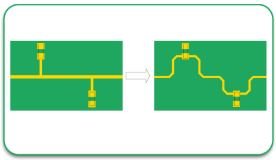
Improper routing can compromise EMI containment. It is essential to follow these rules:

  • Place all high-speed signal trace endpoints close to the circuit.
  • Ensure power supplies do not emit noise-sensitive signal routing.
  • Use noise-cancelling differential pairs for other high-speed signals.
  • In traces never use sharp angles to avoid signal needlessly bouncing. 

Trace and Signal Management

3. Placement of the Components

Considerations regarding component placement help reduce emissions considerably. You should ensure the following.

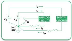
  • Tools and equipment should be grouped functionally. For example, analogue, digital, and power circuits.
  • Sensitive circuits should be placed at a distance from noisy tools like switching regulators.
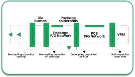
  • Noise from power pins can be suppressed by placing decoupling capacitors in close quarters.

Placement of the Components

4. Power Distribution Network (PDN) Design

Appropriate PDN design greatly ensures power delivery and minimizes electromagnetic interference. Some pointers to keep in mind are:

  • Use several vias to connect to the power and ground planes.
  • Utilize decoupling capacitors to suppress high-frequency noise.
  • Reduce the loop area of power traces to lower emissions.

Power Distribution Network (PDN) Design

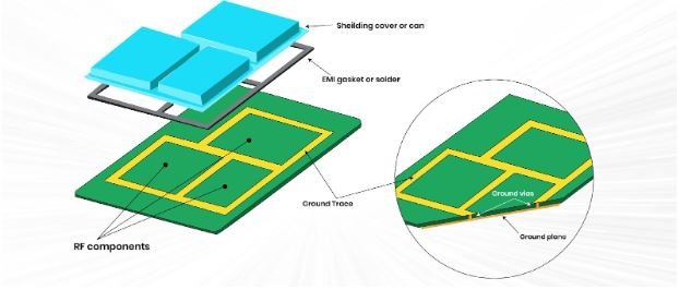
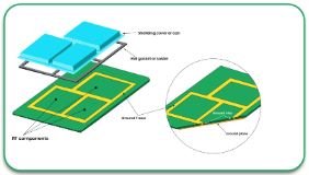
5. Shielding and Enclosure Design

Shielding does not often form part of the PCB arrangement structure, but it is crucial for EMC. You need to collaborate with your PCB vendor to implement the shielding requirements, such as:

  • Metal enclosures that contain the source of interference.
  • Solders cans for covering sensitive parts.
  • Conductive gaskets fill the enclosure gaps.

Shielding and Enclosure Design

Further Methods of EMC Improvement

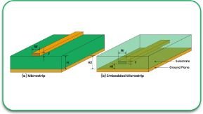
1. Impedance Matching

Reflective signal responses can create interference. Improper impedance matching is usually the cause. To ensure proper matching, follow these:

  • Determining the trace impedance using the material parameters.
  • Impedance-controlled routing on the traces for the speed signals.

2. Split Planes for Mixed-Signal Designs

In mixed designs, the ground plane can be separated to help isolate the analogue and digital circuits, but this must be done with great precision to avoid creating ground loops.

3. EMI Filters

EMI filters are designed especially to eliminate electromagnetic interference in specific appliances. Some common filters are:

  • Ferrite beads.
  • LC filters.
  • Common mode choke.

Mistakes to Avoid in PCB Layout Design

Designers often make errors that can directly affect EMC. Here are some of the most noted mistakes that designers should be aware of:

  • Insufficient Ground Attachment: Weak connections to the ground can cause more EMI as well as noise.
  • Failure to Use Decoupling Capacitors: Not including decoupling capacitors or using the wrong capacitor value can introduce noise to the power supply.
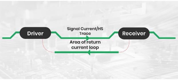
  • Disregarding Return Paths for the Signal: Not considering return currents can lead to the creation of EMI hotspots.
  • Ignoring Thermals: Ultrasonic components can produce thermal noise, which can impact EMC.

Finding the Best PCB Manufacturer

Getting proper EMC compliance is not only dependent on the design stage but also relies on the skills of your PCB manufacturer. A knowledgeable manufacturer can facilitate your work by:

  • Choosing appropriate materials for your design.
  • Using better manufacturing processes to lessen EMI.
  • Performing proper testing to check support for EMC requirements.

At PCB Runners, we are known for providing high-quality PCBs and ensuring compliance with EMC regulations. We work with our clients to proactively adjust the PCB layout design to enhance functionality, reliability, and compliance.

Conclusion

Creating PCB designs that accommodate electromagnetic compatibility is challenging, but it is necessary. With these principles in mind, you can create designs that do not emit unnecessary EMI, tend to signal integrity and adhere to regulations. Each step, from ground plane layout to component placement, is critical to achieving EMC compliance.

Having a reliable PCB manufacturer such as PCB Runners grants you an advantage. Your design will be flawless since PCB Runners specializes in layout design and manufacturing and greatly understands that the boards have to work in challenging situations.

Are you prepared to elevate your PCB designs? Contact PCB Runners to see how we can assist you in attaining EMC compliance and improving the effectiveness of your designs.

FAQs

1. What is electromagnetic compatibility (EMC) in PCB design?

EMC allows a PCB to function without causing or being affected by electromagnetic interference.

2. How does ground plane design affect EMC?

A solid ground plane minimizes the noise and provides a return path for signals that improve EMC.

3. Why is component placement important for EMC?

Properly placed components reduce interference for noisy circuits with sensitive ones, thus greatly reducing the EMI.

4. What do the PCB producers do from their side to ensure EMC compliance? 

A proficient PCB producer can aid in design improvement, material selection, and testing for compliance with the standard regulations on EMC.

5. What are the best practices for minimizing EMI issues in high-speed PCB designs?

Impedance matching, coupling through differential pairs and active decoupling are some of the means to minimize EMI in such designs.

IPC Standards in PCB Design

IPC Standards in PCB Design and Fabrication

Any device with electronic components should significantly pay attention to the design and fabrication of printed circuit boards (PCBs) in order to achieve the desired results. Such devices have been steadily evolving and improving over time. The IPC functions as an international association with over 3000 member companies related to the design, manufacture and assembly of electronic equipment. Quality is not only ensured but also high outcomes are yielded from PCB prototypes using IPC circuit standards boards.

What Are IPC Standards?

The most essential function of IPC is to formulate internationally accepted standards that encapsulate all aspects of PCB designing, fabrication and assembly. These standards are incorporated without any alterations by different nations, as they help measure the defied quality and reliability as well as functionality levels of the APC products. By adhering to IPC standards, all players within the electronics industry, such as designers and fabricators, are operating with set expectations that guarantee contrived results.

Importance of IPC Standards

IPC standards guarantee that PCBs are fabricated to meet stipulated requirements which greatly enhances product reliability as well as performance, leading to improved Quality and Reliability. Some of the Industral benefits to adhering to set standards are consistency, communication efficiency, and overall ensuring that processes and products that were standardized will guarantee interoperability regardless of the fabricating company.

Cost Savings. IPC standards contribute to less expensive production due to lower errors and reduced needed rework.

Environmental Compliance. Many IPC standards emphasize the use of sustainable materials and processes, which is good for the environment.

Important IPC Standards Regarding PCB Design And Fabrication

Some of the most important IPC standards and their relevance are given below.

1. Terms And Definitions (IPC-T-50)

This standard includes and explains all terms and definitions that are relevant to PCB design and manufacture for communication purposes within the industry.

2. Design And Land Patterns (IPC-2221 Series)

The IPC 2221 series provides general design requirements, including effective land pattern design for the most economical board layouts.

3. Substrates And Materials (IPC-4101 Series)

These standards describe the requirements for the PCB’s base materials and substrates, in selection for specific needs and criteria for different uses.

4. Quality And Reliability (IPC-6011 Series)

The rigid, flex, and rigid-flex boards have differing quality and reliability standards, and this overall standard sets criteria for those PCB types.

5. Acceptability Of PCBs (IPC-A-600)

This notably utilized standard intends to define the class of the PCB for its application and the acceptability requirements for completed boards.

6. Soldering Requirements (IPC-J-STD-001)

This standard defines the requirements for soldered electronic assemblies in terms of materials, processes and workmanship.

7. Requirements for Copper Trace and Current Capacity (IPC-2152)

This document outlines the execution of a specific current capacity trace to a PCB design. 

Use of IPC Standards in PCB Design and Prototyping

The application of IPC standards during the PCB prototype phase is critical to achieving the desired quality and performance in the final product. Manufacturers make IPC circuit board standards during design processes so that any evident flaws within the design can be resolved prior to manufacturing.

Expert Insights: Progress of IPC-7351 Standards

A study published on ResearchGate suggests that the design and specification of the IPC-7351 standard are set to supersede the old IPC-SM-782 Surface Mount Design and Land Pattern Standards. IPC-7351 makes necessary changes with respect to design and requirements for assembly and testing, including metric specifications for component dimensions and land patterns, since there are differing geometry requirements based on a product’s use case.

The document includes guidance levels for three standard land pattern dimension levels:

Level A: Exceeds for most digital electronics requiring soldering.

Level B: Moderate balance for more compact electronics.

Level C: Less protrusion for minimum compact electro-mechanical assemblies.

Employing this system of levels makes it possible for manufacturers to customize electronic assemblies and components for optimum efficiency and reliability.

Analysis of Other Industry Comparisons 

UL Standards 

What separates UL standards from others is their focus on safety solely, which is in contrast with IPC circuit board standards that focus on both quality and reliability. It is a lot more integrated in its approach. 

ISO Standards

ISO standards, like ISO 9001, focus on quality management systems without delving into specifics. These standards are too broad compared to IPC standards. Additionally, IPC standards focus on electronic assembly, which makes them ideal for the electronics sector. 

Benefits of IPC Circuit Board Standards

1. Improved Product Performance and Quality 

IPC standards take into account various operating conditions under which a PCB needs to function reliably. Therefore, Argus can maintain solid quality benchmarks. 

2. Uniformity and Flexibility 

Processes that are standardized reduce the chances of design errors and production inconsistencies. 

3. Better Interaction 

Collaboration between designers, manufacturers, and clients is more efficient due to shared standards and definitions. 

4. Cheap Production 

Rework and material waste have decreased, which, along with lean manufacturing, has made IPC standards cheaper to use. 

5. Pro-Environmental 

Many IPC circuit board standards define sustainable materials, which aids the use of pro-environmental practices. 

QAT and Quality Control Procedures Linked to IPC Standards 

Electrical Tests 

No particular assembly’s operational requirements are ignored, as the IPC standards set forth precise testing processes for all components of an assembly. 

Environmental Tests 

The endurance and thermal resistance of PCB products are tested under IPC standards for environmental testing.

Compliance with IPC Standards

Understanding the Standards 

To comply with the IPC standards, one must have a deep comprehension of the IPC standards. This means mapping standards to specific PCB projects. 

Implementation 

Achieving compliance with IPC standards at all levels of PCB design and fabrication activities is fulfilled from the first step to the final test procedures. 

Certification 

IPC certification confirms a company’s commitment to quality and reliability, enhancing trust and credibility with partners and clients. 

Conclusion 

IPC standards drive the dynamism and quality of the PCB industry. From developing the scope of PCB prototypes to ensuring compliance at volume manufacturing, these standards make a tremendous impact on the development of high-quality, reliable and efficient electronics. Through the electronic design and production cycle, one needs to follow IPC standards for circuit boards to remain competitive in the business and deliver electronic products that the market needs. 

The electronics industry is being forced to adopt new standards because of increased competition and changing market dynamics. Embrace IPC standards with PCB Runners to ensure that new products developed will be reliable, efficient, and environmentally friendly.

Maximising High-Speed Signal Transmission with Advanced PCB Reference Plane Techniques

PCBs of high speed are becoming increasingly important for modern systems and devices such as computers, smartphones, and telecommunications equipment that require high data transfer rates. To preserve the integrity and performance of the signal, the reference plane of a PCB has to be designed carefully. This blog aims at advanced techniques of high-speed signal transmission by optimizing the PCB reference plane design in addition to other design parameters for PCB circuit board manufacturers.

Maximising High-Speed Signal Transmission with Advanced PCB Reference Plane Techniques

Importance of Reference Planes to PCB Construction

A reference plane in a PCB acts as a stable voltage plane, typically a solid layer of copper, providing an essential grounding path for high-speed signals. When used alongside signal traces, reference planes are pivotal in shielding traces against electromagnetic interference (EMI).

Reference planes are crucially important in designs with differential pairs, which are used for high-speed interfaces like PCI-Express and Serial ATA. Signal pairs are plus-and-minus combinations of two signals that need a certain level of reference plane to preserve signal quality, limit noise, and improve transmission efficacy.

Problems Encountered in High-speed PCB Design

With the increase in demand for the integrity of high-speed PCB signals, designers of PCBs tend to have a growing list of problems to solve:

  • Complexity in Distribution of Power: Modern parts with multiple voltage levels have created cutouts in reference planes.
  • Impedance Changes: Changes in trace thickness, spacing of differential pairs, or nonuniform reference planes can result in severe signal reflections and information loss.
  • Electromagnetic Interference (EMI): Cuts in the reference plane can create undesired signals that contribute to a signal’s degradation.
  • Crosstalk: The coupling of adjacent traces can result in the loss of a specified signal.

PCB Reference Plane Design Guidelines

The following goals can help structure the PCB reference plane design for efficient high-speed signal transmission:

1. Solid, Uniform Planes

Do not allow cuts or gaps in the reference plane. Breaks in planes lead to signal distortion due to unstable impedance paths.

2. Efficient Use of Ground Layer

Ground planes should be placed next to high-speed signal layers in addition to signal layer loops. This configuration helps improve the quality of the signals while minimizing signal loops.

3. Differential Pair Routing Control

Traces should maintain equal spacing from the reference plane to help control differential pair routing. The above setup enhances impedance control and allows the reduction of signal suffrage.

4. Via Reduction

Reducing vias helps preserve high-speed PCB signal integrity, as each via discontinuity can have a distinct impact on high-speed signals. Where required, place them away from return paths to help maintain signal integrity.

5. Guard Important Signals From Interference

For traces with high EMI and crosstalk, it would be best to use shielding or guard traces to reduce interference in environments where noise is rampant.

6. Confirm The Results of The Impedance Computation

Employ simulation software for the network to compute, in addition to confirming the results pertaining to trace impedances and differential impedance, which is usually 100 ohms in high-speed situations.

Impact of Slits on Signal Transmission

Due to the advancement of multi-power designs, cuts in the reference plane are often necessary. Understanding the effects of these cuts on signal propagation is equally important in order to reduce negative consequences.

Experimental Findings

One of the effects noted was that the insertion of a 5mm slit in a microstrip reference plane resulted in a differential increase of approximately 6 ohms. The Sdd21 measures showed a significant recession of propagation signals when the common mode impedance (Zcom) was lower.

Within this study, the authors presented mathematical models to demonstrate how the effect of the slits. This information can assist designers when devising a plan to alter the design that seeks to enhance the transmission characteristics.

Primary Measurement Methods of High-Speed PCB Signals

For optimal Testing and Measurement, a high-end standard is followed by PCB circuit board fabricators. Some of these techniques include:

1. Time Domain Reflectometry (TDR)

TDR gives Time Domain Reflectometry the ability to reflect pulses from a line communication and perform analysis of transmission. To facilitate the interpretation of problem areas like slits in reference planes.

2. Transmission and Crosstalk Analysis

Broadband network analyzers do not measure transmission losses or crosstalk. This information is crucial in helping designers measure how different facets of the signal design affect its integrity.

3. S- Parameter Analysis

Static S-Parameter synthesis allows the Designer to perform S-Parameter simulation and pristine quality verification of Signal Transmission. This may also include suggesting alternatives to the existing assembly or routing novel transmission paths.

Practical Approaches to High-Speed Signal Integrity

The techniques to tackle PCB reference plane design disruption problems:

1. Stitching Capacitors

The introduction of stitching capacitors can solve the placement of slits or gaps. These slits and the stitching capacitors provide a routing low impedance during high frequencies.

2. Differential Pair Shielding

Employ shielding where routing of differential pairs across a slit is considered.

3. Simulation and Modeling

Use prediction tools to diagnose, anticipate, and rectify shortcomings before it is too late. Due to the introduction of simulation technologies, designers now have the ability to evaluate how modifications will affect the overall high-speed PCB signal integrity prior to the physical production stage.

4. Design Rule Checks (DRC)

Ensure that reference planes are relevant and consistent throughout the entire structure via thorough DRCs with special emphasis on high-speed signal design guidelines as supporting criteria.

Emerging Trends in High-Speed PCB Design

Newer devices and higher data rates must match technology’s evolution, requiring a more refined PCB design style. Advanced materials like low-loss laminates are rapidly emerging in the market for high-speed designs. Furthermore, engineers are solving the complex challenges of high-speed PCB signal integrity with the help of powerful simulation tools and artificial intelligence-based design optimization.

PCB circuit board manufacturers need to be at the forefront of innovation to stay competitive and provide advanced technologies.

Conclusion

To integrate maximum permittable signal transmission speeds in PCB designs, reference plane techniques need to be modified strategically. Consistency in reference planes, optimal routing of differential pairs, and rigorous testing are some of the steps that PCB circuit board manufacturers need to take to design for the modern high-speed world.

By carefully planning and following best practices, PCB circuit board manufacturers can overcome design challenges while achieving high-speed PCB signal integrity and effective performance in demanding environments.

Stay updated with such information at PCB Runners.

Materials for HDI PCBs

High-Performance Materials for HDI PCBs

High-density interconnect (HDI) PCBs have transformed the electronics world by making it possible to design smaller and more powerful devices. They are widely utilised in telecommunications, aerospace, automotive, and consumer electronics. 

These advanced PCBs’ ultra-high functionality and dependability are achieved through the use of high-performance materials and innovative solder mask materials. In this blog, we will focus on essential materials employed in the manufacturing of HDI.

The Role of Advanced Materials in HDI PCBs

Substrate Materials: Beyond Traditional FR4

Flame-retardant epoxy laminate FR4 was and still is the preferred base material for the majority of PCBs. However, due to the miniaturisation of devices and their increasing performance, FR4 has been found inadequate in various thermal and electrical specifications. Thus, the shift is taking place towards the usage of polyimide, PTFE (polytetrafluoroethylene), and ceramic-based substrate materials.

  • Thermal Stability: Ideal for use in extreme conditions, such as the automotive and aerospace sectors, Polyimide and ceramic-based substrates are able to operate under extreme environments.

Delamination

  • Electrical Performance: PTFE is a low-loss dielectric material with a low dielectric constant and dissipation factor, easily incorporated into 5G and superfast communication systems.
  • Miniaturisation: The ability to achieve intricate structures is possible due to advanced ceramic substrates with excellent mechanical strength and low thermal expansion, which can provide punctual and reliable performance.

Miniaturisation

These innovations make the next generation of electronic gadgets smaller, quicker, and more efficient than ever before.

Expert Insight: Advanced Materials for the Growing Needs of a PCB

Modern electronics are far too advanced to handle using older, outdated materials. This is specifically highlighted in the ResearchGate paper “Advanced Materials in PCB Manufacturing,” which includes this excerpt:

“Along with FR4, there were many materials above it that catered to a large number of applications but slowly, over the years, became irrelevant as devices started to shrink in size and outperformed the older models. The industry has now moved on to polyimide, PTFE, and ceramic-based substrates, which allow unparalleled thermal stability and durability while having blunt electrical components.”

Such developments are critical for industries that depend on compact size, high frequency, and high-speed communication as well as accuracy and reliability.

Conductive Materials: Reliable For Signal Transmission

At the moment, copper is the only material used in high-density interconnect PCBs since it is the most reliable and conductive. In dense layouts where more intricate designs are required, the copper on the micro vias and fine lines serve the purpose well.

Solder Mask Materials: Performance Protection and Improvement Enhancements

In HDI PCBs, the solder mask is one of the important layers to prevent damage from the environment, solder bridging, or contamination, as well as protect the device. The development of solder mask materials for high-density designs is crucial because they can maintain a high level of resolution and thermal stability.

Key Properties of Advanced Solder Masks:

  • Precision: Finer lines and spaces are critical.
  • Resistance: Endures degradation over several cycles of soldering.
  • Low Dielectric Values: Elevate the signal preservation in high-frequency uses.

The advancement of new solder mask materials with better thermal and electrical qualities is crucial.

Final Thought

The choice of advanced substrates, solder masks, and any additional components is essential for the high-density interconnect PCBs. Improved thermal control, enhanced electrical performance, and increased support for the miniaturisation of electronic components.

At PCB Runners, we take pride in using the newest materials and advanced manufacturing methods to create the highest-quality high-density interconnect (HDI) PCBs that exactly meet your needs. From advanced substrates to high-performance solder masks to other comprehensive PCB needs, we are ready to assist.

Reach out to us today to discover more about HDI PCBs and how we could assist your next venture.

FAQs

Q1: What are HDI PCBs?

A1: HDI Printed Circuit Boards (PCBs) have high wiring density relative to the surface area of the board, meaning they can link more components together at a time. They employ finer lines and spaces, reduced vias, and enhanced component density.

Q2: Why is material selection important in HDI PCBs?

A2: The materials selected determine the electrical performance of the PCB, the thermal management capability of the laminate, and the mechanical stability. These factors directly relate to the PCB’s reliability and functionality.   

Q3: What are the advantages of using advanced solder mask materials for HDI PCBs?

A3: The latest solder masks are less susceptible to damage from exposure to external elements while maintaining signal stability with excellent resolution, low dielectric constants, and high thermal stability.  

Q4: Why do advanced substrates enhance PCB performance?

A4: Advanced polyimide and ceramic substrates offer improved thermal and electrical performance, compact design support, and enhanced performance due to higher stability. 

Flexible PCBs for Flexible Displays

Flexible PCBs for Flexible Displays: Transformation of the Electronics World

Recently, there has been a significant introduction of enhanced features in consumer electronics—flexible displays. From curved televisions to foldable smartphones, the designs are sleek and offer some modern features.

Flexible Printed Circuit Boards (FPCBs) enable the core structure of these devices and their displays. In this blog, we’ll explore how flex and rigid PCB technologies are essential for modern, flexible displays and their benefits across industries.

What Are Flexible Printed Circuit Boards?

FPCBs, or flexible PCBs, are designed to bend without losing their electrical function. Unlike Traditional rigid PCBs, these are more modern and are crafted from substrates such as polyimide, which provide them with the needed shape.

Types of PCBs Used in Flexible Displays

Flex PCBs are ultra-flexible circuit boards used in devices that require folding, twisting, or curving features.

Rigid-Flex PCBs: The circuit board is made of a combination of flexible and rigid circuits. True to its name, it offers enhanced strength whilst maintaining adaptability.

Both types, as mentioned above, are widely termed compact and lightweight components.

The Importance of Flexible PCBs within Flexible Displays

A flexible display needs to have parts that are light in weight, compact, and effective. Conventional rigid PCBs cannot meet these specifications because of their inflexible structure. Flexible PCBs offer a solution because they have the following characteristics:

  • Bendability: The feature necessary for smartphones and mobile wearables.
  • Space Efficiency: FPCBs use less vertical space, making it possible for manufacturers to construct ultra-thin displays.

Space Efficiency

  • Lightweight Structures: This feature is beneficial for portable devices such as tablets and fitness trackers.

Lightweight Structures

  • Durability: Flex circuits perform consistently over time, even after repeated cycles obending.

Key Materials Used in Flexible PCBs

The kind of materials selected for flexible PCBs for displays determines the performance and reliability of the PCB.

Substrate Material:

  • Polyimide is the material of choice because of its flexibility and high thermal stability.
  • Polyester is also used for cost-sensitive applications, although it has a lower resistance to thermals.

Conductor Material:

  • Copper is widely used because of its good electrical conductivity.
  • Copper foils can be laminated with the polyimide flexible substrate to produce robust circuit traces.

Adhesive Layers:

  • Epoxy or acrylic adhesive serves as the conductive layer and the polyimide substrate adhesive.

Methods of Construction for Flexible PCBs

Building FPCBs aims to achieve flexible display capabilities, and the following procedures do it:

1. Cleaning and Preparing Substrate

The flexible substrate is cleaned and laminated with an adhesive layer and a protective coat.

2. Etching and Patterning

The Circuit patterns are created with Photolithography techniques, followed by excess copper removal through etching.

3. Application of External Circuitry

The multilayer integrated FPCB structure is constructed by laminating single circuits.

4. Plating and Drilling

Sequential plated through holes (Vias) are drilled for layering, and then electrical connections are plated to the Vias.

5. Quality Assurance and Testing

Flexible PCBs have high reliability and performance which comes from extensive testing as well as industry standard incorporation.

Usage of Flexible PCBs in Screens

The adoption of flex and rigid PCB technologies has remarkably increased, enabling their use in flex and bendable displays:

1. Smart Phones with Attachments

Flexible PCBs allow folding designs of displays as they bend around the corners seamlessly.

2. Smart Wearable Devices

FPCBs in smartwatches can be used because of their advanced ergonomic features.

3. Televisions with Curved Screens.

FPCBs are less fragile and the increase in display FPCBs allows for more broad usage in modern televisions.

4. Screens in Automobiles

The interface used in modern cars, with clusters and infotainment systems made with flexible FPCBs, has created customer-integrated curved displays.

5. Medical Devices

Today’s medical monitoring devices can be made smaller and more portable, owing to lightweight flexible PCBs that can adapt to a variety of displays.

Advantages of Flexible PCBs for Display Applications

Integrating FPCBs into flexible displays has many benefits:

  • More Productive: Allows for diversity in the shapes of devices.
  • Increased Reliability: Endures bending and moisture.
  • Lowered Difficulty for Assembly: Reduced use of connectors and interconnects lowers assembly time.
  • Electrically Efficient: Shorter signal paths enhance electrical performance.
  • Financially Convenient: Reduced material usage and compact designs lower production costs.

Challenges and Solutions

There is always a price to pay for certain benefits, in this case, the manufacturing process of FPCBs for flexible displays:

1. Material Handling

Challenge: The flexible substrates are easily breakable and unsightly to deal with.

Solution: Use of automation and specialized handling tools for effective placement.

2. Signal Integrity Issues

Challenge: Signal loss from older traces.

Solution: Careful design and impedance control can help reduce signal losses.

3. Heat Management

Challenge: Slender devices have less surface area to cool off.

Solution: Using thermal vias and heat-dissipating materials.

Expert Insights

FCBs, or Flexible Circuit Boards, are vital components in contemporary electronics systems. They are present in mobile phones, laptops, smartwatches, cameras, and even robotic arms. These circuit boards are especially beneficial in applications with constrained spaces where standard Printed Circuit Boards (PCBs) cannot be utilized.

In comparison to conventional PCBs, FCBs possess several advantages like increased reliability, decreased weight, and more space efficiency. Nevertheless, they come with certain challenges, particularly during the installation and repair procedures of a system. During installation, FCBs are stressfully bent at multiple points which is significantly more than rigid PCBs. This stress, which gets compounded due to the system’s repeated bending, eventually leads to breakage.

The complexity increases when it comes to FCBs because of their structure and the requirement to model both the installation and operational phases of the model. Thus, in this study, a methodology for modelling these phases was created using Ansys Mechanical. The simulation determined the stresses induced during both phases and assessed the fatigue life of the FCBs after the operational phase. 

Two types of models were studied: a Rigid-Flex PCB, which consists of a flexible circuit between two rigid PCBs, and a Flex FCB cable with no rigid components. For both models, shell elements were used to mesh the thin FCB structures, which rotate and bend significantly and are therefore subjected to large loads.

Trace mapping streamlined the intricate geometry of vias, solder connections, wires, and other electronic CAD components. This technique modelled the geometry as dielectric layers and mapped the metal fraction onto these layers so that the effects of the traces were accurately modelled. The models were bent at an angle of 180 degrees in order to study the fatigue due to this bending load. 

For the FCB cable, there was some additional stress analysis conducted during the installation phase, because the stresses developed at this stage do have an overall bearing on the fatigue life of the cable. Rigid surface bodies were utilized in the simulation to deform the FCB cable into its final installed position to model real-world conditions.

This research also performed a High-Performance Computing (HPC) scalability analysis to provide optimal simulation performance. This analysis, in turn, determined the appropriate division of the processor cores against the time necessary to reach an accepted solution. This made it possible to simulate the model faster and more efficiently.

This study enriches knowledge of FCBs’ behaviour during the installation process and operation. In addition, it serves as an accurate predictor of performance and fatigue life, enabling engineers to design more effective FCBs for different electronic purposes. By preemptively spotting certain failure modes, the methodology increases the reliability and lifespan of these important components.

Conclusion

Flexible Printed Circuit Boards (FPCBs) are changing the landscape of display technology, bringing advancements such as flexible smartphones, curved TVs, and other smart wearable devices. The fusion of flex and rigid PCB technologies allows manufacturers to satisfy the increasing market need for multifunctional electronic devices. Anticipating future trends within the industry, FPCBs will be the basis for advanced next-generation displays for many years to come.

PCB Runners is a leader and supplier of high-quality flex and rigid PCBs for various applications across several industries. With our experience and reputation, we provide dependable and affordable PCBs specifically designed to meet our customers’ needs.

Frequently Asked Questions

Q1: What are flexible PCBs used for?

A: Foldable smartphones, wearable devices, automotive displays, and medical devices all utilize flexible PCBs due to their lightweight nature and easy adaptability.

Q2: What materials are used in FPCBs?

A: Polyimide substrates, copper conductors, and protective solder masks are commonly used materials.

Q3: What is the difference between flex and rigid PCBs?

A: Flex PCBs are adaptable to bending and twisting, whereas rigid PCBs have no flexibility. Rigid-flex PCBs offer the best of both worlds.

Q4: What challenges are associated with FPCBs?

A: Advanced material handling, signal integrity concerns, and thermal control are the major challenges with FPCBs. However, advanced manufacturing techniques can solve these problems.

Q5: Why choose PCB Runners for flexible PCBs?

A: When it comes to flex and rigid PCBs, PCB Runners has unmatched industry experience, top-tier materials, and specific peripheral solutions.

Designing Military-Grade PCBs

Designing Military-Grade PCBs For Maximum Durability

Military active PCBs (printed circuit boards) need to pass grueling tests to endure the straining conditions of a theater of war and work effortlessly. The high working temperature, vibrations, and even moist conditions are some of the hurdles these specialized circuit boards need to overcome. 

This blog will discuss the strategies employed by leading PCB manufacturers to fabricate military-grade circuit boards with exceptional strength and toughness.

What Makes a Military Circuit Board Different?

As opposed to standard PCBs, military circuit boards need to operate flawlessly even in extreme conditions like rapid/ sudden changes in temperature, exposure to certain chemicals, and high-amplitude vibrations. To cater to these unusual demands, military PCBs are designed following strenuous requirements like IPC Class 3 and MIL-PRF-31032.  

The focus lies on selecting materials, design techniques, and manufacturing processes that offer the best reliability. Also, circular shape requirements have broadened the applicability of circuit boards in the military field.

Key Materials for Military PCBs

For a military-grade PCB, high-performance materials that can resist overpowering heat, chemicals, and even mechanical strain are essential to support. Some common materials are: 

High-Tg Laminates: Isola FR408HR and DuPont Pyralux are specified materials that resist temperatures over 200 degrees Celsius.

high tg

Metal Core Substrates: Aluminum and copper cores aid in the rapid dissipation of heat.

Metal Core Substrates

High-Frequency Materials: High-frequency signals are well handled by materials such as the Rogers 4000 series. 

Expert Insights 

Military-grade PCBs have some of the toughest standards in electronics. The PCBs must endure severe conditions, function well under stress, and be capable of continual operation without any failure. 

One of the strictest standards for these boards is MIL-PRF-31032, which covers everything global boards fail to defocus on. Everything from the design of the PCB, the material chosen, and even the method of manufacturing is set in stone. But it doesn’t stop there- military standards define the set components that leave very little breathing space. 

Moreover, there are regulations outlined that govern entirely the assembly of the boards. Quality control guidelines are also elaborated to check that the set high-performance thresholds are met.

Thermal Properties: The Importance of Tg

The glass transition temperature (Tg) is crucial for military PCBs. It represents the temperature beyond which the material softens, losing its rigid structure. For military applications, designers recommend materials with a Tg of at least 170°C to 200°C or higher.

Material Type Tg Range
Low Tg 130°C – 160°C
Medium Tg 160°C – 200°C
High Tg 200°C +

Top Design Rules for Military PCBs

Here are essential design considerations when creating a military circuit board:

1 Surface Mount and Land Considerations

  • Defects on the sides of rectangular lands should not exceed 20%.
  • Lands for circular mounts (BGAs, for example) should strive to have minimal defects, ideally below 10 percent of the circumference. 

2. Porous Plating Method Hole Specifications

  • For the required thickness, copper plating should be a minimum of 80% of the thickness. 
  • Voids in the plating should not be more significant than 5% of the PCB thickness. 

3. Via Copper Plating 

  • For filled vias, there should be no voids or bumps that can give access to internal layers. 
  • Moisture damage will be prevented with proper copper plating of vias. 

Additional Tips for Designing Durable Military PCBs

Use heat compounds and heat-resistant enclosures to control excessive heat. 

  • Component Isolation: High, more sensitive components should be placed away from low-frequency parts to minimize interference. 
  • Simulations before Layout: Simulations should be done to measure performance in real-life situations. 

Clock signals should be covered with aluminum shields to limit interference. 

The use of chemical resistant and anti-moisture conformal coatings can be used to shield the components. 

The Role of Circular Circuit Boards in Military Applications

Due to their compact, efficient features, circular circuit boards are becoming increasingly prevalent in military applications. These boards have a lot of advantages, such as: 

  • Space Efficiency: These are essential to installations that need compact electronic integration. 
  • Concise Signal Traces: The radius of the board reduces trace lengths, thus enhancing performance. 
  • Mechanical Strength: Because of their unique shape, mechanical stress is evenly distributed, giving them strength. 

Choosing the Right PCB Manufacturer for Military Circuit Boards

To ensure compliance with military specifications, select ITAR-registered PCB manufacturers.

  • A reliable PCB partner should: 
  • Abide by the IPC and MIL standards. 
  • Have the necessary equipment to manufacture multi-layer and circular circuit boards. 
  • Conduct adequate tests and quality control measures. 

Here at PCB Runners, we focus on military-grade PCB manufacturing, emphasizing quality, durability, and precision to satisfy the toughest requirements.

Conclusion

Achieving a military-grade PCB means stricter policies on materials used, layout design, and standards set. And with any circuit board, be it traditional or circular, strength and dependability come first. No question, working with a reputable PCB manufacturer guarantees that your military circuit boards will work in the most demanding situations. 

If you need a PCB manufacturer who is sensitive to the intricacies of military applications, PCB Runners is your perfect solution. 

Reach out today to find out more about our services for custom military circuit board construction. 

FAQs 

What are military circuit boards? 

Military circuit boards are specially designed PCBs that can sustain extreme conditions, such as high temperatures and powerful mechanical forces. 

What materials are used for military PCBs? 

Commonly used materials include high-Tg laminates, metal core substrates, and high-frequency Rogers 4000 series. 

Why are circular circuit boards used in military applications?

Circular circuit boards can save space, enhance the efficiency of signal paths, and improve the distribution of mechanical stress. 

How do I select a suitable PCB manufacturer? 

You should seek out ITAR-registered manufacturers that specialize in military-grade PCBs and have a strong compliance record with IPC standards. 

Which standards are military PCBs subjected to? 

These include, among others, the seminal MIL-PRF-31032 and IPC Class 3, which guarantees quality and reliability in the design and construction of the PCB for military purposes.

Choosing the Right Stackup for Your HDI PCB Design

The design of a High-Density Interconnect (HDI) PCB is essential today due to the evermore shrinking and demanding electronic parts. The complex structure of an HDI PCB, along with its unique fabrication techniques, helps PCB manufacturers fulfill the needs for increasingly smaller and more powerful devices. 

As with most design work, one of the most important parts of it is assembling the correct stack up. This blog will discuss various stackup configurations and how to select the most appropriate one.

HDI PCB Design

What is an HDI PCB Stackup?

An HDI PCB stackup is the configuration of the conductive and non-conductive layers of a printed circuit board patterned out on the PCB. It decides the ordering of signal routing, power distribution, and the mechanical and electrical operations of the entire board. 

Optimize stackup design approaches to ensure the reliability of signals, reduction of electromagnetic interference (EMI), and improve overall strength of the PCB.

Why is Stackup Selection Essential?

Choosing the correct stackup is fundamental to maintaining the power distribution while ensuring signal integrity in an HDI PCB design. Signal loss, boosted level of crosstalk, and more challenging procedures during fabrication can all stem from poorly assembled stackups.

Stackup Selection Essential

Key factors influenced by the stackup include:

Routing Density: Efficient use of layers can support complex routing paths.

Signal Integrity: Proper stackup reduces noise and interference.

Cost Efficiency: The number of layers and types of vias affect manufacturing costs.

Common HDI PCB Stackup Types

Most PCB companies use the following three stackup types for HDI PCBs.

1. Standard Lamination with Vias or Plated Through Holes (PTHs)

This type of stackup uses a simple lamination process with traditional through-hole vias connecting all layers.

Advantages:

  • Cost-effective for designs with fewer layers (28 layers or less).
  • Simplifies the manufacturing process.

Disadvantages:

  • Limited routing capabilities for complex designs.
  • Not suitable for high pin-count Ball Grid Arrays (BGAs) with pitches below 0.8 mm.
  • Challenging to manage high-density signal paths.

2. Sequential Lamination with Plated Through, Blind, and Buried Vias

This configuration includes blind and buried vias in addition to through vias.

Advantages:

  • Improved routing capabilities compared to standard lamination.
  • Reduced via stubs and smaller via diameters.

Disadvantages:

  • Higher fabrication costs.
  • Limited practical layer count, typically up to three layers.
  • Still less efficient for complex high-density interconnect applications.

3. Lamination Buildup with micro vias

This advanced stackup is especially suitable for high-density designs involving fine-pitch BGAs.

Advantages:

  • Enables higher routing density with fewer layers.
  • Smaller trace widths and via diameters.
  • Better power and signal integrity.
  • Cost-effective for high-frequency, high-density boards.

Disadvantages:

  • Requires advanced manufacturing processes.
  • Initially, it can be more expensive than traditional methods.

Benefits of Lamination Buildup with Microvias

Many leading HDI PCB manufacturers, including Rush PCB Inc., recommend lamination buildup with microvias for advanced high-density interconnect designs.

Why Choose Microvias?

  • Higher Routing Density: Microvias allow designers to use fewer layers while achieving dense routing.
  • Improved Signal Integrity: Smaller vias and shorter signal paths reduce interference and noise.
  • Cost Efficiency: Despite initial costs, the reduced layer count and improved performance lower overall expenses.
  • BGA Compatibility: Ideal for boards with multiple large BGAs with pitches below 0.8 mm.

IPC Standards for HDI PCB stackups

The IPC-2315 standard categorises HDI stackups into six types:

  • Type I: Laminated core with a single microvia layer.
  • Type II: Laminated core with microvias, blind, and buried vias.
  • Type III: Laminated core with two or more microvia layers.
  • Type IV, V, VI: More advanced and expensive configurations.

Let’s take a closer look at the most common types.

HDI Type I

  • Structure: Laminated core with a single microvia layer.
  • Vias: PTH and blind vias, but no buried vias.
  • Use Case: Suitable for less complex high-density interconnect designs.

Limitations:

  • The aspect ratio for PTH vias must be less than 10 for reliability.
  • Thin FR-4 dielectrics may delaminate during lead-free soldering.
  • It’s not ideal for large boards with multiple BGAs.

HDI Type II

  • Structure: Laminated core with microvias, blind, and buried vias.
  • Vias: Stacked or staggered microvias.
  • Use Case: More suitable for complex designs than Type I.

Limitations:

  • Outer layers are often restricted to power/ground planes.
  • Less effective for single buildup layer routing.

HDI Type III

  • Structure: Laminated core with two or more microvia layers.
  • Vias: Stacked or staggered microvias, blind, and buried vias.
  • Use Case: Best for complex, dense multilayer PCBs.

Advantages:

  • Greater routing density.
  • Outer layers are available for power/ground planes.
  • Ideal for large boards with multiple BGAs.

Limitations:

  • Higher fabrication costs.
  • Still constrained by PTH and thin FR-4 dielectric limitations.

Choosing the Best HDI Stackup

When designing a HDI PCB, the following should be considered when selecting a stackup.

1. Demands of the Application

The complexity of the design, frequency of operation, and routing density should be examined in detail. The Type III stack-up is preferred for high-performing applications with dense routing.

2. Parts Choice

In cases where many fine-pitch BGAs are present, micro-via base stackups are preferred due to better routing.

3. Cost Constraints

Achieve performance targets without going over budget. Even though microvia stackups have a higher upfront cost, they are often the most cost-efficient in the long run due to fewer layers and better yield.

4. Signal Integrity and Power Distribution

Select the stackup that will optimise minimum interference. Lamination buildup with microvias is best for high-frequency applications.

Conclusion

The selection of the right stackup will greatly benefit your HDI PCB design. From the most basic design to a complicated board filled with fine-pitch BGAs, each stackup type has advantages and disadvantages that must be considered.

Working alongside a capable PCB manufacturer can aid in the choice of stack up, optimising the design and ensuring that industry requirements are met. Lamination buildup with microvias will always remain the best approach for HDI PCBs because of high routing density, good signal integrity, and low cost. 

Choosing the right stackup, along with advancements in technology, will definitely increase a designer’s competitiveness in the field of high-density interconnect designs.

For such crucial information about PCB design, sign up to our updates at PCB Runners.

Assembling High-Quality Rigid-Flex PCBs

Advanced Techniques for Assembling High-Quality Rigid-Flex PCBs

To keep up with the demand for modern electronics, industries are pivoting towards Rigid-Flex PCBs, which are a step in the future. These multilayered versatile circuit boards are an advanced version of traditional circuit boards. They combine the best features of rigid PCBs and flexible circuits, making them appropriate for applications with intricate shapes, lower weight, and superior strength. 

Achieving a successful assembly of Rigid-Flex PCB requires an understanding of the key material features, some sophisticated engineering processes, and creative assembly techniques.

A Walkthrough of Rigid-Flex PCBs

Rigid-flex PCBs consist of integrated rigid and flexible regions on the same board structure. Their main advantage over conventional PCBs is that they allow reduced connector counts, better signal integrity, and more excellent design maneuverability. This makes them extremely useful for aerospace, medical, wearable devices, and other consumer electronics. 

Categories of Rigid-Flex PCBs

Rigid-flex PCBs can be categorized based on their structure:

  • Single-Sided Rigid-Flex PCBs: Flexible layer copper traces are only present on one side.
  • Double-Sided Rigid-Flex PCBs: Copper traces are added to both sides of the flexible layer. 
  • Multi-Layer Rigid-Flex PCBs: Composed of insulating layers with multiple conductive materials added to increase intricateness and greater routing density.

RIGID FLEX

Material Selection for Rigid-Flex PCBs

Selecting appropriate materials for a rigid-flex PCB fabrication process affects the intended performance and reliability. These materials include the cover layer, adhesive, copper foil, and the substrate.

Recommended Materials

  • Polyimide Films: These materials are best for use as they have superior thermal stability, dielectric properties, and flexural strength.
  • Foils: Flexible copper foils of low thickness provide good electrical conductivity and reasonable mechanical flexibility.
  • Adhesive: Polyester and polyimide adhesives are frequently utilized as a solution to dimensional variability.
  • The selection of appropriate materials can improve robust mechanical properties and enhance dimensional stability and performance during the assembly process.

Key Production Processes

The fabrication of rigid-flex PBMs is one of the most challenging processes in PCB assembly. Its primary goal is to obtain high-quality results through precision and careful control.

Cleaning and Surface Preparation

Patterning with high precision in flexible PCBs requires high-skill surface preparation due to the difficulties involved in cleaning flexible PCB materials. Since flexible PCB materials are soft and thin, a mechanical approach will not provide adequate surface value.

Preferred Techniques

  • Electrolytic Cleaning: The melting electrolytic alloy delivers good roughness value while providing sufficient cleanliness to the surface.
  • Micro-Etching: Fine spacing between copper traces with tight tolerance can be achieved by micro-etching.

Layer Alignment

Many materials, such as polyimide, show increased moisture absorption, which can lead to PCB dimensional instability. Flexible, placed multi-layer PCB components require higher precision in flexible layer alignment.

Alignment Techniques

  • Alignment Holes: These lower the chances of layers being placed incorrectly.
  • X-Ray Drilling: X-ray drilling enables improvements for the drilling offsets, and fixing them determines where the added holes should be placed.

Multiflex Plating

Multiflex plating techniques reinforce critical areas in a rigid-flex PCB. In addition to improving mechanical strength, these techniques also improve electrical conductivity, making it easier for the PCB to bend and endure dynamic loads.

Assembly of Rigid-Flex PCBs

The assembly of rigid-flex PCBs is more difficult than assembling rigid boards because they are lightweight and very thin.

Fixtures and Carriers

During surface mount technology procedures, assemblers use specialized fixtures and carriers to hold the flexible parts of the board.

Common Fixtures

  • Board Trays: Used to keep the board in shape and its position.
  • Baking Fixtures: Reduce the absorption of moisture before assembling the boards.
  • Electrical Test Fixtures: Different tests are performed, which include a credibility check.

Adjustments in the SMT process

  • Low-Temperature Soldering: Flexible components are not thermally damaged by soldering.
  • Component Placement: Careful handling reduces assembly deformation.

Panelization

The rigid-flex PCBs are usually panelised to facilitate assembly. After assembly, the separate boards are punched out one by one from the assembly panel.

Ensuring Product Quality

Because a rigid-flex PCB has challenging tasks, the product quality must always be high.

Key Quality Control Measures

  • Soldering Reliability: Achieves a mechanical bond that remains intact.
  • Anti-Static Precautions: To avoid interfering with electronics sensitive to static.

RoHS and Lead-Free Compliance

For the environment, RoHS and lead-free regulations are more stringent than for any other industry. In that regard, the rigid-flex PCB manufacturing process has to be updated to work with high soldering temperatures. This means that process and material selection must be made with great care.

Cost Considerations

Unlike standard rigid boards, a rigid-flex PCB’s assembly process is more costly, which means the entire assembly procedure is more complex, requires fixtures, and takes longer to complete. But thanks to process and technology advancements, the cost is slowly but surely lessening.

Factors Affecting Cost

  • Fixures and accessories: A baseline for custom fixtures.
  • Manufacturing Periods: Benchmark timelines for precision processes.
  • Staffing Requirements: Skilled assembly labour.

Expert Insights on the Future of Flexible and Rigid-Flex PCBs

With the continuous improvement in technology, more and more challenges in electronic design need to be solved. Flexible and rigid-flex printed circuit boards (PCBs) are perhaps the most disruptive innovation in the world of electronics because they dramatically outperform rigid boards in both ease of use and are lightweight and compact. 

Flexible PCBs can be twisted and bent, which allows for the fabrication of small and light devices. Meanwhile, rigid-flex PCBs offer controlled flexibility while retaining the structural strength of rigid boards, providing robustness for designs intended for the automotive, medical, aerospace, and even consumer electronics industries. Rich functionality and durability have allowed the invention of modern designs, which are smarter and more compact than ever.

Their versatility and potential are illustrated by the increasing adoption of flexible and rigid-flex PCBs in wearables, electric vehicles, and IoT devices. For instance, in automotive systems, these PCBs allow manufacturers to fulfill the requirements of advanced driver assistance and in-vehicle connectivity due to their compact size. In medical devices, flexible PCBs enable the creation of highly conformable wearable health monitors. 

Ongoing automation and materials innovation will enable manufacturers to overcome challenges such as increased costs and complicated processes. The ability of these PCBs to increase efficiency and functionality will determine the future of electronics design, from smart devices to aerospace technologies.

Conclusion

Rigid-flex PCBs are essential for many applications due to their increasing requirements in engineering sophisticated electronic devices. Meticulously implemented multiflex plating, precise layer alignment, and advanced assembly techniques allow manufacturers to produce high-quality, defect-free PCBs. Although there are higher upfront costs, the long-term savings achieved from their performance, durability, and design flexibility make rigid-flex PCBs cost-effective.

Contracting professionals in PCB assembly maximize the efficiency and accuracy of your project by implementing the newest techniques. For an effective and smooth rigid-flex PCB assembly service, work with a reputable PCB manufacturer like PCB Runners who has considerable experience in this area.

Achieving Higher Accuracy In Multilayer PCB Testing with X-Ray Inspection

The integration of electronic components into a single device has escalated the need for dependable multilayer printed circuit board (PCB) testing. These boards serve as the foundation for contemporary electronics, containing complex connections and components within several layers. 

The operation of these devices is fault-free only after adopting sophisticated testing methods. Automated X-ray inspection (AXI) is increasingly being used and has developed into an essential gear for testing these devices upon completion. This article highlights how automated x-ray inspection PCB performs, its benefits, and how it allows for stringent control of checks.

automated x ray inspection pcb

The Complexity of Multilayer Printed Circuit Boards

Multilayer PCBs are key to most advanced applications, such as telecommunications, aerospace, automotive, and even healthcare devices. With several conductive layers encased in insulating material, these boards have improved function and performance. However, the level of sophistication of these boards brings forth problems during the manufacturing stage. These problems include hidden solder joint defects, component misalignment, and via-incomplete stages.

Advanced testing techniques such as optical inspection and electrical testing seek to overcome these challenges. Unfortunately, neither approach is adequate for addressing the possible multilayered internal defects hidden inside the PCB. Hence, automated X-ray inspection PCB can prove to be a significant advancement in the industry.

How Automated X-Ray Inspection PCB Works

AXI systems harness high-energy X-rays to penetrate through and reveal the internal structures of a PCB. Unlike visual inspection, which only looks at the surface, X-rays can expose hidden defects located within the board’s layers. These systems create sophisticated images displaying the quality of solder joints, the placement of components, and other possible defects.

Typically, the procedure consists of the following stages:

How Automated X-Ray Inspection PCB Works

  • Image Acquisition: Capturing images at pre-defined angles using X-ray projection on the PCB.
  • Data Interpretation: Using X-ray imaging to perform defect recognition with artificial intelligence algorithms.
  • Defect Recognition: The system captures voids, missed alignments, and solder bridging as problems highlighted by the system.

AXI is especially effective in discovering defects in Fine-Pitch Components and High-Density Interconnects (HDI) because those flaws are difficult to see with the naked eye.

Expert Insights: Enhanced Testing Techniques

As noted in an article from ResearchGate, older X-ray techniques such as Digital Radiography (DR) often struggle with multilayer printed circuit board testing. Overlapping images provided by DR makes patient diagnosis very challenging since it becomes impossible to view every layer distinctly or to find clear defect locations.

To overcome the previously described issues, the study proposes an innovative technique that uses the following steps:

  • Oblique Angle Irradiation: The surface of the PCB is irradiated with X-ray at an angle that is not perpendicular to the surface.
  • Rotational Projection Imaging: The board undergoes rotation while projection images are taken.
  • Slice-by-Slice Reconstruction: Each layer of the image is constructed from detailed cross-sections revealing pertinent information for every single component of the target object.

This approach remarkably boosts the overall accuracy of defect analysis and provides insight into the construction of the PCB’s internal layers.

Advantages of Multilayered PCB X-Ray Inspection

1. Non-Destructive Testing

The primary benefit of automated X-ray inspection PCB is completely damage-free inspection. Manufacturers can examine PCBs without the risk of inflicting any damages that would hinder repair or rework.

2. Enhanced Defect Detection

A very diverse number of defects can be widely identified using X-ray inspection, including but not limited to:

– Voids in solder joints.

– Missing or misconfigured components.

– Inadequate or improperly constructed vias.

– Short circuits or solder bridges.

3. Improved Quality Control

X-ray inspection reduces defect and scrap rates, resulting in improved overall product reliability by catching mistakes earlier in the production cycle.

4. Automation for Efficiency

Quality remains high while meeting the demand of a high volume of production due to rapid and accurate testing provided by automated X-ray systems.

5. Layer-Specific Analysis

Other techniques than traditional methods offered detailed layer-specific analysis and the ability to gain insights not previously accessible. This research gate study has covered the machine learning reconstruction method, for example.

Use of PCB X-ray Manufacturing Process

Xray technology, particularly AXI, is used at almost all stages of PCB manufacturing:

  • Prototyping: A step that validates that a design does not have any glaring mistakes at the start.
  • Mass Production: Doing production in bulk with a guarantee of consistency in the quality of output.
  • Defect Investigation: Determining the reasons and failure parts for the PCBs found to be defective.

Aerospace, telecommunications, and automotive industries are big users of the technology due to established quality requirements.

From Supreme Materials to PCs: Testing with a Challenge

As bulk production of PCBs becomes commonplace, testing becomes increasingly challenging, which is one reason why advanced materials have to be properly tested. As devices become smaller and more powerful, materials like solder masks and high-frequency laminates create big problems.

AXI systems will have to change to improve the materials that can be inspected on judgeable terms. Quality monitoring and check-ups of non-conductive or super-dense layers will be the basic requirements for ensuring quality maintenance.

New Agendas in Xray Inspection Technologies for PCBs

1. 3D X-Ray Imaging

Level and volumetric data that can be attained with newer 3D X-ray technologies allow for extremely accurate analysis of complicated structures.

2. AI Based Analytic

Along with more profound levels of scrutiny, the use of artificial intelligence and machine learning for automated X-Ray Inspection systems in ramping up deficiency distinctions, while keeping the rate of false alarmers in check.

3. Smarter Automation

Improvements in automation will be made in future systems, further boosting the inspection speed while minimizing the need for operator involvement.

Conclusion

Methods such as automated X-ray inspection (AXI) are necessary. To achieve higher precision in multilayer PCB testing, TX-ray inspection nondestructively examines the internal structures of modern PCBs, which determine the reliability and functionality of contemporary electronic devices.

PCB Runners is a well-known provider of comprehensive PCB solutions and offers design, manufacture, and testing services. Our experience in multilayer PCB production and new inspection methods guarantee that our customers receive dependable, high-quality products.

Give us a call today to discover how we can assist your next project by utilizing these advanced PCB solutions.

FAQs

1. What is a multilayer printed circuit board?

A multilayer printed circuit board (PCB) has more than one conductive layer with insulating materials in between the layers; these PCBs offer enhanced functionality for more sophisticated electronic devices.

2. What exactly is automated X-ray inspection (AXI)?

AXI helps visualize the internal structure of PCBs using X-rays, which makes defect detection easier as defects are concealed within the assembly structure, hence improving the quality of the product.

3. Why is multilayer PCB’s X-ray inspection so important?

X-ray inspection can capture defects obscured by external layers and is necessary for ensuring product reliability and high endurance performance.

4. What do you think the defect AXI can reveal?

AXI can detect voids in solder joints, misplaced components, incomplete vias, and short circuits.

5. What goes into the maintenance of quality in multilayer PCB production provided by PCB Runners?

Runners PCB uses the latest inspection efforts, like AXI, to keep its quality standards at a high level and produce reliable PCB solutions.

How to Match Your PCB Design with the Right Surface Finish?

Choosing the right surface finish affects the overall quality, functionality, and reliability of printed circuit boards. The finish is intended to be a protective coating to prevent soldering and contact pads from becoming oxidized or sullied. Quite simply put, copper surfaces that are not covered are prone to oxidizing, rendering them useless for the efficient soldering of components or reliable electrical contacts.

This article covers various types of PCB surface finishes, their selection processes, and, of course, which designs are right for which surfaces. The wrong decision regarding the surface finish could create assembly problems or cause them later in the PCB’s life, so making an informed choice is essential for your PCB’s success.

How to Match Your PCB Design with the Right Surface Finish?

Key Information You Need

A number of considerations, including design, application, and environment, must be taken into account when deciding on the PCB surface finish. Commonly used finishes are listed below, along with guidelines for PCB Circuit Board Manufacturers on their use:

Lead-Free Hot Air Surface Levelling (HASL)

    • Best for: General-purpose applications, especially when solderability and cost are priorities.
    • Advantages:
      • Good solderability
      • Affordable and robust for multi-step assembly
      • Excellent for larger board surfaces
    • Drawbacks:
      • Extra thermal load due to the submersion in liquid solder
      • Less flat compared to other finishes
      • Not ideal for fine-pitch components

Lead-Free Hot Air Surface Levelling (HASL)

Electroless Nickel/Immersion Gold (ENIG)

  • Best for: Designs requiring flat surfaces, long shelf life, or applications like keypads and wire bonding.
  • Advantages:
    • Excellent flatness and solderability
    • Suitable for fine-pitch and sensitive components
  • Drawbacks:
    • Higher cost
    • It can be brittle under stress or vibration

Electroless Nickel/Immersion Gold (ENIG)

Immersion Silver (ImAg)

  • Best for: Prototypes and short production runs where flatness and solderability are needed.
  • Advantages:
    • Flat and smooth surface
    • Good solderability
  • Drawbacks:
    • Susceptible to tarnishing in sulfur-rich environments
    • Shelf life can be limited depending on storage conditions

Immersion Silver (ImAg)

30u” to 70u” Hard Gold for Edge Connectors

    • Best for: Edge connectors that need to withstand wear and tear.
    • Advantages:
      • Durable and resistant to abrasion
      • High-quality electrical contact
    • Drawbacks:
      • Only applied to specific areas (edge connectors)
      • Higher cost and limited application

30u” to 70u” Hard Gold for Edge Connectors

Carbon Ink Surface Finish

    • Best for: Switch contacts, foil keyboards, and cross-over conductors.
    • Advantages:
      • High mechanical strength
      • Good electrical conductivity
    • Drawbacks:
      • Less common and not suitable for general-purpose applications

Carbon Ink Surface Finish

Benefits and Application

Choosing the right surface finish for your PCB ensures that your design can handle the demands of both the manufacturing process and the operational environment. 

Here are some practical benefits: 

  • Enhanced Reliability: A proper finish can protect gold from oxidation and contamination. It also ensures that soldering and electrical connections are permanent. 
  • Improved Assembly: Flatness is essential for placing fine-pitched components. Some finishes help, like ENIG, which is used for soldering gold, while HAL is best for bigger components. 
  • Cost-Effective: A surface finish that is not too expensive but can withstand the conditions is perfect for non-specific applications like HAL.
  • Long-Term Wear: Hard gold-plated surface finishes protect edge connectors from excessive physical abuse and provide durability.

These considerations, coupled with the type of components, environment, and projected shelf life, make it possible to increase the efficiency and durability of PCBs.

Expert Insights

The ionic contamination of printed circuit boards (PCBs) with different surface finishes was systematically evaluated using ionograph testing at room temperature. The study examined three PCB surface finishes applied to copper substrates: (i) hot air solder leveling (HASL LF), (ii) electroless nickel immersion gold (ENIG), and (iii) organic surface protectant (OSP), in combination with two flux types, EF2202 and RF800. 

Among the PCBs without soldered components, the ENIG finish with an 18 µm thickness exhibited the lowest average contamination level, measured at 0.01 µg NaCl/cm². Conversely, PCBs with soldered components showed higher contamination levels, reaching 0.29 µg NaCl/cm² for the HASL LF finish of the same thickness. The introduction of fluxing agents resulted in the highest contamination values across all surface finishes.

The study further investigated the impact of phosphorus content in the Ni-P layer of the ENIG finish on ionic contamination. Among PCBs with gold coatings, the lowest surface contamination level (0.32 µg NaCl/cm²) was observed for the Ni-2-5%P layer, while higher contamination levels were recorded for Ni-11%P (0.47 µg NaCl/cm²) and Ni-8%P (0.81 µg NaCl/cm²). 

In contrast, PCBs without gold coatings exhibited their lowest contamination levels (0.48 µg NaCl/cm²) at 11% phosphorus content, whereas increased contamination levels were observed for lower phosphorus contents, with values rising to 1.98 µg NaCl/cm² at 8% phosphorus content. The findings suggest that PCBs with an Au finish generally exhibit lower contamination levels compared to their non-Au counterparts, contributing to enhanced reliability of electronic assemblies by mitigating the risk of failures associated with current leakage and corrosion caused by surface contaminants.

FAQs

What is the most suitable surface finish for surface mount components of low pitch?

ENIG (Electroless Nickel/Immersion Gold) is best for supplementing fine-pitch components with flat surfaces and easy solderability.

What do I do to keep Immersion Silver from tarnishing?

PCBs should be stored in sulfur-free environments to prevent tarnishing, and protective finishes can benefit from hermetically sealed packaging.

Why is Hard Gold used for edge connectors?

Because edge connectors endure frequent contact, Hard Gold is the most favorable option because it has a high wear rate.

What is the shelf life of ENIG?

Compared to other surface finishes, ENIG has a longer shelf life; therefore, it is better suited for long-term storage or designs that are not immediately assembled.

Is it possible to use more than one finish on a single PCB?

Yes, a variety of finishes may be applied to several areas of the PCB, such as Hard Gold on edge connectors and HAL on the remainder of the board.

Conclusion 

Selecting an appropriate surface finish for your PCB is crucial for its performance during and after assembly. For long-term reliability, ENIG, HAL, ImAg, or Hard Gold can all be selected, but the option you select should depend on your design requirements and the environment it will be subjected to.

Are you unsure which surface finish to use on your PCB? Do not hesitate to contact us. We at PCB Runners will guide you so that you achieve your project objectives.