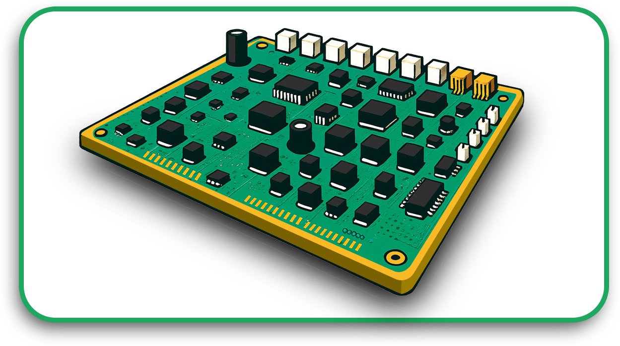
With regard to PCBs, stakeholders at all levels will know that sensor PCB boards are one of the most impactful parts of modern electronics. Sensors work seamlessly today; they detect motion, manage the temperature in industrial regions, or sense gas for safety.
PCBs that serve functional sensors are expected to be accurate, dependable, and incredibly efficient. With the advancement in technology, sensors are PCBs have become one of the most integral components enabling devices to interface with their surroundings cognitively.
With such complexity, engineers expect the utmost precision from the device’s components. Therefore, each type of PCB sensor should be differentiated appropriately to enhance its performance and functionality.
Relying on the right sensor type selection, PCB design optimization, and high-quality manufacturing increases an electronic device’s ability and accuracy while ensuring durability.
For expert PCB design and manufacturing services, look no further than Runners PCB. They provide high quality sensor PCB boards customized to meet your unique requirements.
What Are PCB Sensors?
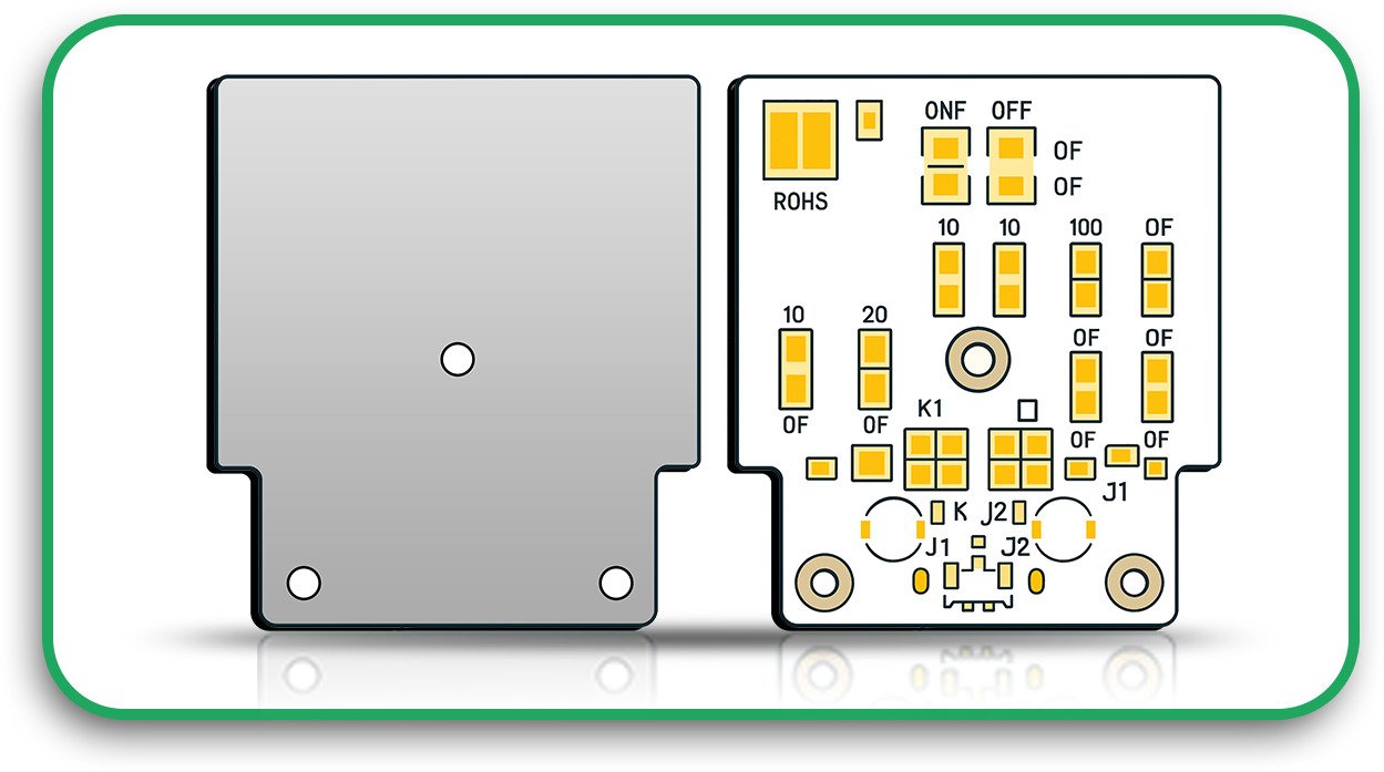
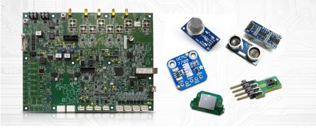
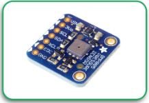
PCB sensors are an assembly of electronic parts integrated into a sensor PCB board for effective measuring and detecting environmental changes such as pressure, motion, humidity, or temperature. These functional sensors can transform physical or chemical changes into electricity signals, which can then be processed.
The functional capacitor, for instance, detects motion through a change in capacitance excited by variations in electric fields or temperature. The energy from a motion is transformed into electricity and changes into varying frequencies for easy processing.
How PCB Sensors Work
- Detection: The sensor recognizes the change from the set environmental factors.
- Conversion: Variances recognized are converted into electrical signals.
- Processing: A microcontroller or processing unit understands the signal.
- Action: The system notes a signal and, consequently, provides the appropriate reply.
Importance of PCB Sensors
- Enhancements System Performance: Allows for more accurate control and effective management.
- Design Based On Economy: Minimizes the need for additional external sensors and extra cabling.
- Trustworthiness: Makes sure that the devices function properly in practical conditions.
Types of PCB Sensors
1. Temperature Sensors
Temperature recording devices are important for proper functioning under various temperature conditions in industrial automation, medical devices, and home appliances.
Common Types of Temperature Sensors
- Thermal sensors Measure extreme temperatures and are usually employed in industries and space crafts.
- RTD, resistance temperature detectors – Commonly used in scientific instruments because of their high accuracy.
- Thermistors: Found in air conditioning and refrigeration units and other electrical appliances.
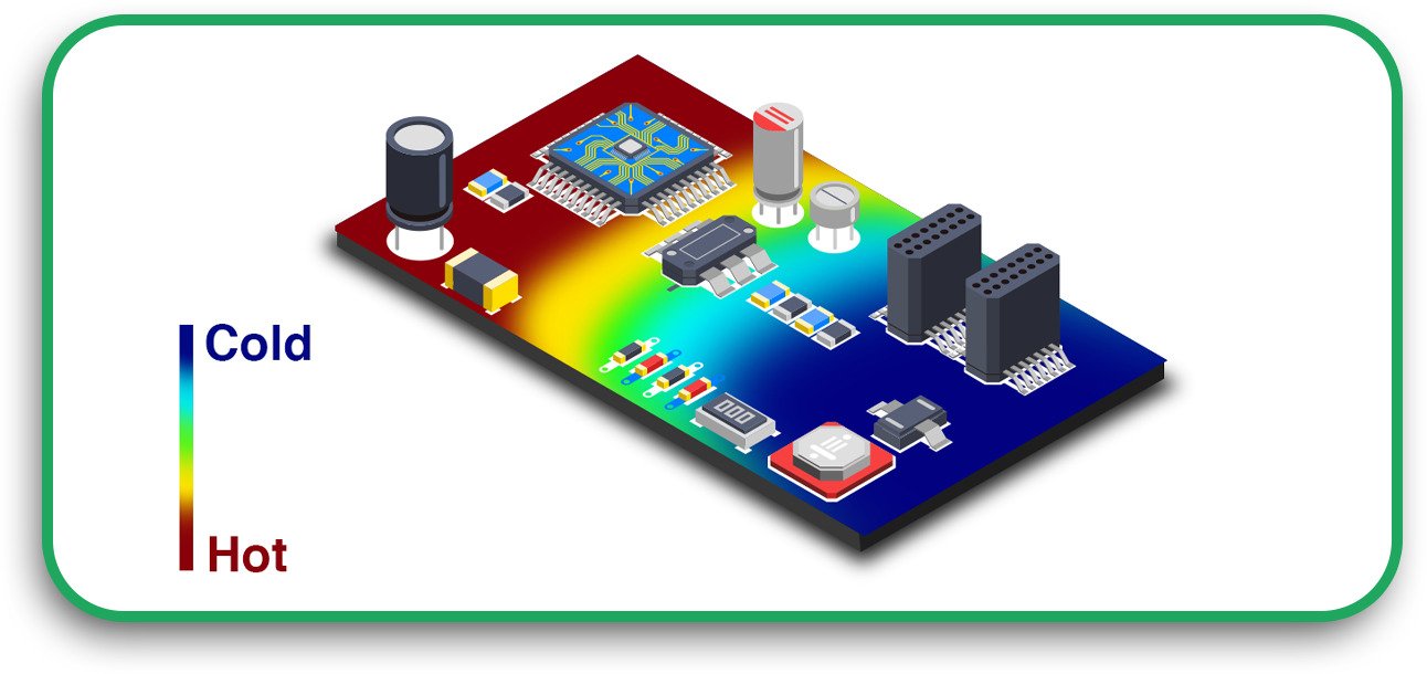
Effect On PCB Performance
- Overall thermal management of the electronics improves the reliability in high power applications.
- Increased product life by lowering the operating temperature.
2. Pressure Sensors
These sensors can measure changes in the pressure of gases and liquids. They have found extensive applications in automotive, medical and the industry.
Key Applications
- Automotive – Checks the provided tyre pressure and fuel tanks.
- Medical Devices – Monitors blood pressure and equipment for artificial respiration.
- Industrial System – Pneumatic and hydraulic system controls.
Effect On PCB Performance
Makes certain that pressure readings are correct for both safety and efficiency.
Minimizes equipment malfunction by controlling pressure changes.
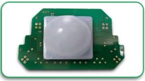
3. Motion Sensors
These sensors sense movement and position, which are important features in smartphones, robotics, security devices, and wearable technology.
Different Types of Motion Sensors
Accelerometers: Detect linear movements and tilt position changes.
Gyroscopes – Measures rotational angle. Mostly used in drones and navigating devices.
Infrared Sensors – Movement detection from the heat emitted by the body.
Effects on PCB Performance
Allows the automation of smart home and industrial applications.
Improves user interaction with the technologies in gaming and wearable electronics.
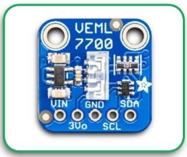
4. Light Sensors
Light sensors measure illumination and are widely used to control the brightness of lights, displays, and other optical instruments.
Uses
- Smartphones: Make it possible to change the brightness of a display according to ambient light conditions.
- Industrial Automation: Used for identifying faults in assemblies.
- Energy Saving Lighting: Smart systems for LED lights, including dimming control.
Effects on PCB Performance
- Decreases the energy consumption.
- Improves visibility as well as user experience in electronic devices.
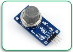
5. Gas Sensors
Gas Sensors are an effective means of detecting dangerous gases in industrial, automotive, and household safety applications.
Main Uses
- Industrial Plants: Detection of leaks from toxic gases.
- Automobiles: Used for controlling the Emission system.
- Smart Homes: Smoke and carbon monoxide sensors.
Effects on PCB Performance
- Mitigates health risks through monitoring air quality.
- Assists industries in meeting environmental health and safety requirements.
6. Humidity Sensors
Sensors that measure humidity are important in Agriculture, Pharmaceuticals, and HVAC systems.
Applications
- Ventilation: HVAC and Air conditioning systems.
- Farming: Cattle ranching and soil watering systems.
- Medical: Medicines are safe from moisture issues.
Effect on PCB Performance
- It enhances the effectiveness of sensitive climate control work.
- Guarantees stability and shelf life for products in the pharmaceutical domain.
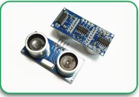
7. Distance Measuring Sensors
Distance-measuring sensors classify the proximity of objects without direct contact. They are used in automation, robots, and other technology.
Categories of the Distance Measuring Sensors
- Feature Sensors– Recognizing non-metallic items.
- Metal Sensor – Recognizes micromagnets by induction electromagnetic field.
- Sound Sensor – Measures distance with sound.
Effect on PCB Performance
- Contactless control functions for PC-like devices and smart cards.
- Enhances accuracy and productivity of devices in industrial robotics.
Expert Insights
Integration of PCB technology with biosensors substantially transforms the health sector by permitting fast and ultra-reliable detection of biological and chemical substances in seconds. The same concept applies to building PCBs. Making electrodes and sensing elements for biosensors utilizes the same logic. With mass-produced electronics, some construction methods can be used for biosensors. These methods provide high stellar rates, save money, and are easier to manufacture. Standard PCB technology lowers cost and makes it easier to manufacture.
With the ability to directly pattern electrodes and other electrical components onto a sensor’s PCB board, the accuracy and efficiency of signal detection have greatly improved. Thus, it has been easier for industries like medical diagnostics, environmental monitoring, or even food safety to incorporate the technologies of printed circuit board manufacturing for the development and integration of biosensors.
One of the major innovations in this area is the integration of microfluidics structures with thin film PCB sensors that provide highly compact and portable real-time monitoring and analysis. The incorporation of low-profile detection systems on a sensor PCB board allows for point-of-care medical diagnostics, health monitoring, and even industrial biosensing systems. But there are still many issues to tackle like improving biocompatibility, increasing sensitivity, and more cost-effective construction techniques.
Newer methods with cutting-edge materials, multilayer PCB configurations, and hybrid manufacturing may help overcome the obstacles which remain the focus of ongoing research. It is clear from this research that as the demand for cheap, highly efficient biosensors increases, the PCB manufactures responsibility in the innovation of this market will intensify.
Important Guidelines for Sensor PCB Project Management and Execution
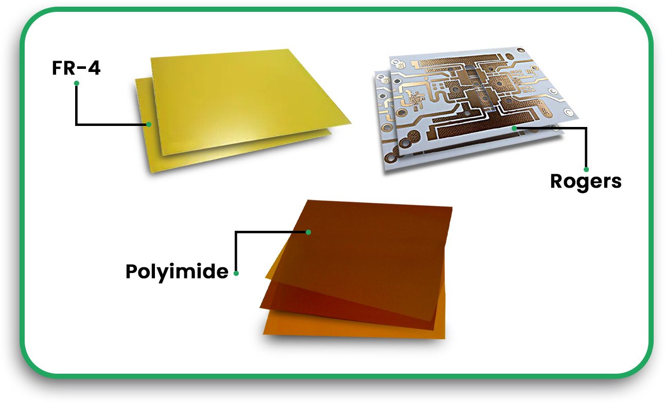
Choosing PCB Material:
- FR4 for regular sensors.
- High-frequency PCBs for RF sensors.
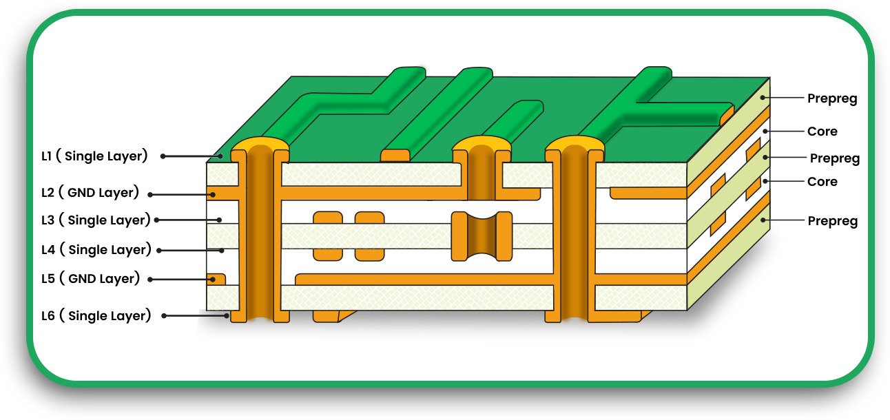
Strategic Sensor Location:
- Minimization of interaction with other components.
- Stability of thermal changes for sensitive elements like temperature sensors.
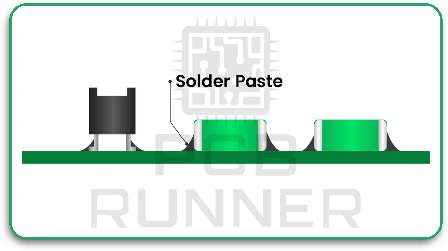
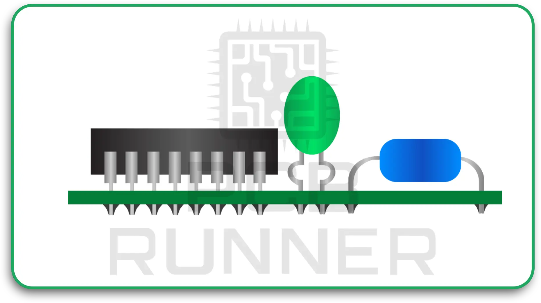
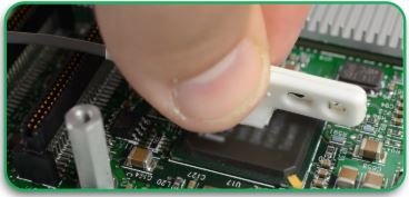
Proficient Methods of Production:
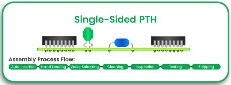
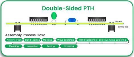
- Through-hole and Surface Mount Technology (SMT) are done with great precision.
- Automated systems were used for testing and accuracy calibration.
- Trends on the PCB sensor technology of tomorrow
- Ultra-small sensors to be used in compact devices.
- Wearable sensors are meant for medical and fitness purposes.
- Machine learning sensors work in real-time to make important decisions on the spot.
- Integration of the Internet of Things to enable smart homes and industrial automation.
Final Thoughts
With the increased development of smart sensors, reliance on electronic engineers, PCB designers, and manufacturers will expand as they implement high-performance sensor PCBs within their designs. The selection of appropriate sensors, PCB layouts, and quality manufacturing will characterize the new epoch of highly efficient, reliable, and intelligent devices.
We at PCB Runners know the importance of proper PCB sensor design and manufacturing. Give us a call to see how we can transform your ideas into realities.