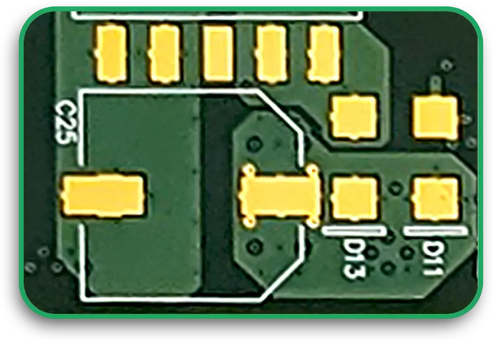
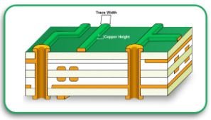
PCBs support modern, electronically sophisticated equipment at their core. The thickness of PCBs is a key metric as it contributes to a product’s overall performance, durability, and manufacturability. Maintaining a standard PCB thickness helps guarantee coordination across various applications.
Industries spanning consumer electronics to aerospace and automotive need to be well-versed in multilayer PCB thickness standards. Circuit board manufacturers pay attention to these aspects so that their products serve the market’s prerequisites while improving the production regime. This article aims to discuss an overview of PCB thicknesses, their engineering, and industrial best practices for PCB manufacturing.
Importance of PCB Thickness
The thickness of PCBs is not just treated as a ratio – it scopes up an entire PCB’s electrical performance, thermal characteristics, and mechanical performance. Here are some of the factors that are most directly impacted due to the variation in PCB thickness:
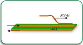
- Electrical Performance: The thickness of the PCB layers can affect the measurement of components such as signal integrity, impedance control, and power distribution.
- Heat Dissipation: PCBs that use high-power applications during work achieve a proper PCB layer thickness, which facilitates thermal conductivity alongside heat dispersion.
- Mechanical Strength: Environmental stresses, mechanical vibrations, and even assembly processes tend to damage a PCB, and thus, a suitable thickness needs to be determined.
- Manufacturing Compatibility: The standard thickness allows the design to be procured for universal software or systems.
Standard PCB Thicknesses
While PCB thickness can vary depending on application requirements, the electronics industry follows specific standard thicknesses. The most common thicknesses include:
| Layer Count | Standard Thickness (inches) | Standard Thickness (mm) |
| Single-layer | 0.031″ – 0.062″ | 0.8mm – 1.6mm |
| Double-layer | 0.062″ | 1.6mm |
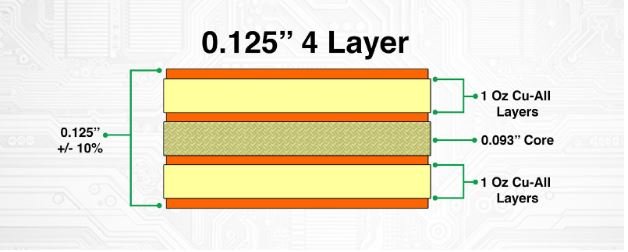
| Multilayer PCB (4-6 layers) | 0.062″ – 0.093″ | 1.6mm – 2.4mm |
| Multilayer PCB (8-10 layers) | 0.093″ – 0.125″ | 2.4mm – 3.2mm |
| Specialty PCBs | Custom thickness | Application-specific |
These standard thicknesses ensure compatibility with industrial PCB manufacture processes, enabling easy assembly and reliability.
Factors Influencing the Selection of PCB Thickness
PCB thickness selection ranges from functional requirements to material selections. Considering these other aspects may help streamline the design process:
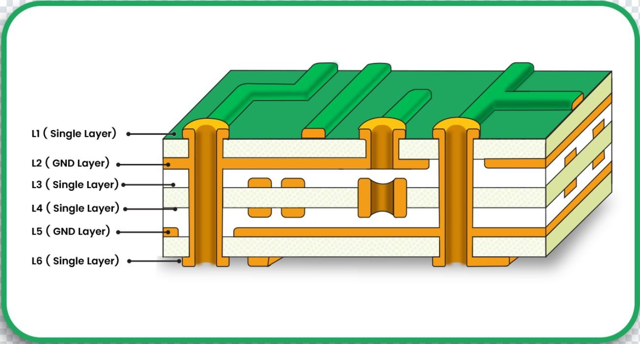
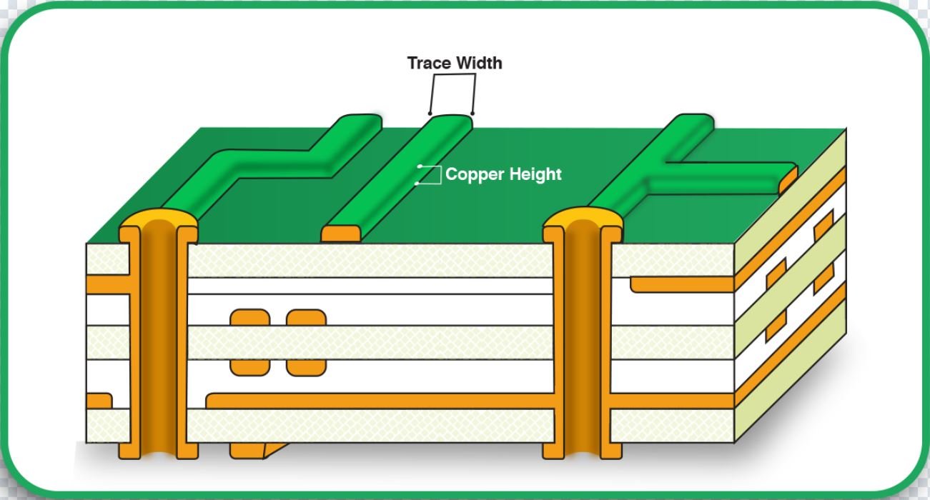
1. The Number of Layers
Dielectric and copper layers affect the overall thickness of Multilayer PCBs. Thicker boards are essential for the telecommunication and aerospace industries, where high-performance applications are needed.
2. Copper Thickness
Various copper weights utilized in a PCB will impact its thickness. The standard copper thickness includes the following:
- 1 oz copper – Common for most consumer and industrial PCBs. (~35µm per layer)
- 2 oz of copper – Used for power electronics and high-current applications. (~70µm per layer)
- 3 oz of copper and above – Ideal for high-power industrial applications.
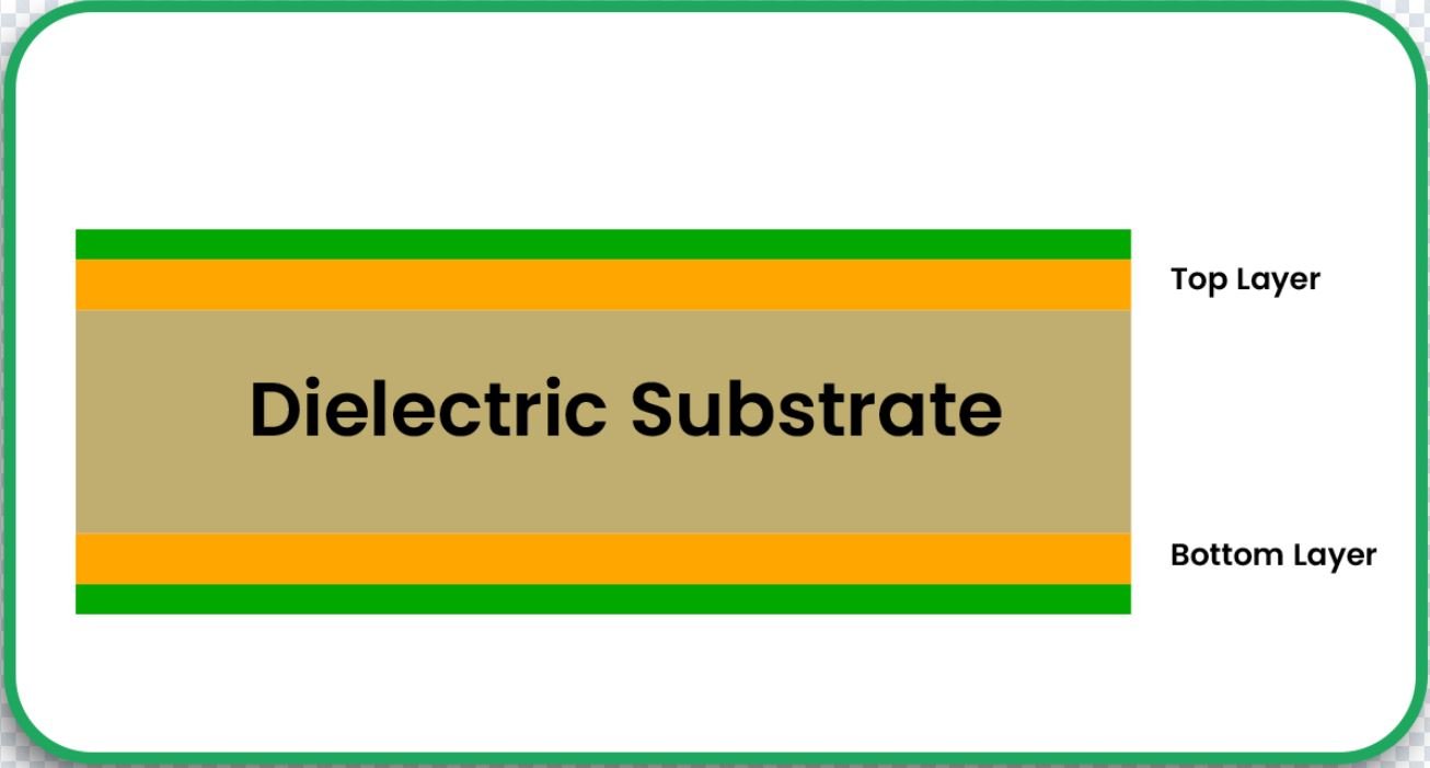
3. Substrate Material
Copper substrate materials like FR4, polyimide, or even ceramic materials impact the general thickness of the PCB. To control the dielectric constant and ensure that signal transmission is optimized, PCB circuit board manufacturers use materials with varying dielectric constants.
4. Mechanical Consideration
Flexibility versus Rigidity: Industrial applications require that thick PCBs (>1.6mm) provide rigidity while thin PCBs (<0.8mm) for flexible electronics.
Thermal Expansion: No materials should warp for an electronic PCB during drastic temperature changes.
5. Application-Specific Requirements
An example includes the automotive and aerospace industries, which have stringent thickness specifications meant to ensure reliability in a harsh environment. Most PCB design software commonly used in the industry enables engineers to create matching PCBs that satisfy these requirements.
How to Choose the Right PCB Thickness
Choosing the right thickness for a PCB is all about optimizing simultaneous criteria:
- For Consumer Electronics: A PCB thickness of 1.6mm is a good compromise between manufacturing convenience and sturdiness.
- For High-Power Applications: Thicker copper layers of 2 oz or more on the PCB dissipate heat more efficiently.
- For High-Frequency Applications: Thinner PCBs increase high-speed performance and minimize signal loss.
- For Industrial PCB Manufacture: Heavy-duty PCBs need to be specially designed for shock and vibration resistance.
Industry Standards for PCB Thickness
Standards organizations monitor the thickness of PCBs so that dimensional regularity among manufacturers is kept. Some of these existing industry standards are:
- IPC-2221 – IPC generic design standard for PCBs, which includes thickness requirements.
- IPC-6012 – Qualification and performance standard for rigid PCBs.
- MIL-PRF-31032 – PCB military performance specifications for a hostile environment.
- ISO 9001 & AS9100 – Quality management certification relevant to industrial PCB manufacture.
Difficulty with Controlling the Thickness of PCBs
1. Tolerances on Manufacturing
Standard practices often involve some variation in thickness, which is further complicated by material and fabrication issues. PCB circuit board manufacturers are expected to accommodate these tolerances.
2. Bending and Warping
Heat, especially during the reflow soldering phase, usually results in the bending of thinner PCBs. Proper reinforcement techniques greatly reduce this.
3. Consideration of Cost
Processing thicker boundaries and IoT PCBs increases the material expense or requires special processing, which further raises production expenses. Engineers always struggle between performance and expense.
New Directions in Achieving Optimization of Thickness for PCBs
The incorporation of such new technologies leads to more complex designs for PCBs and simplifies the problem of thickness optimization as follows:
- New and Innovative Materials: These materials are structures such as ultra-thin PCBs that are used in medical implants and wearable-type compact devices.
- AI in PCB Design: Incorporating AI into standard PCB design software allows the user to instantly check compliance with requirements for set thicknesses.
You have asked a highly trained source who possesses comprehensive knowledge of electronics and has provided insightful quotes.
Conclusion
It is essential to understand the thickness of the PCB in order to ensure other components work with it. Working with multilayer PCBs, consumer devices, or even industrial electronics will be easier if you stick to the standard thickness, as it makes it easier for manufacturers to make their PCBs. By using industry-standard PCB design software, engineers are able to achieve an optimum balance with respect to PCB thickness in terms of performance, durability, and manufacturability. As the need for stronger, thinner, and more efficient PCBs increases, so will the changes in the electronics industry.
Work with PCB Runners to get customized Industrial PCBs that solve problems. Send us a message today!
FAQs
What is the most common thickness of a PCB?
The most common one is 1.6mm (or 0.062 inches) as is commonly used in industrial and consumer devices.
Can you customize the thickness of the PCB?
Yes, most of the PCB circuit board manufacturers will cater to custom thicknesses depending on the application requirements.
In what ways does signal integrity get impacted by the thickness of a PCB?
Thinner PCBs have less signal loss in high-frequency applications, while thicker PCBs are more suitable for power handling and durability.
Which materials do affect the PCB thickness?
Substrate materials such as FR4, polyimide, and metal core, along with the copper weight, determine the final thickness of the PCB.
Which software is the most suitable for strict PCB thickness specifications?
Like other engineering disciplines, Altium Designer, KiCad and Eagle are examples of PCB design software that aid engineers in designing PCBs with set thickness requirements.