Circuit Board for Fault

How to Check a Circuit Board for Faults: Tips and Tools for Diagnosis

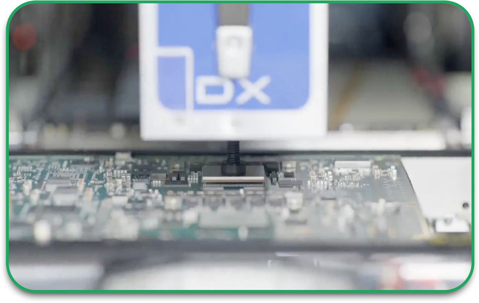
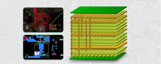
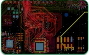
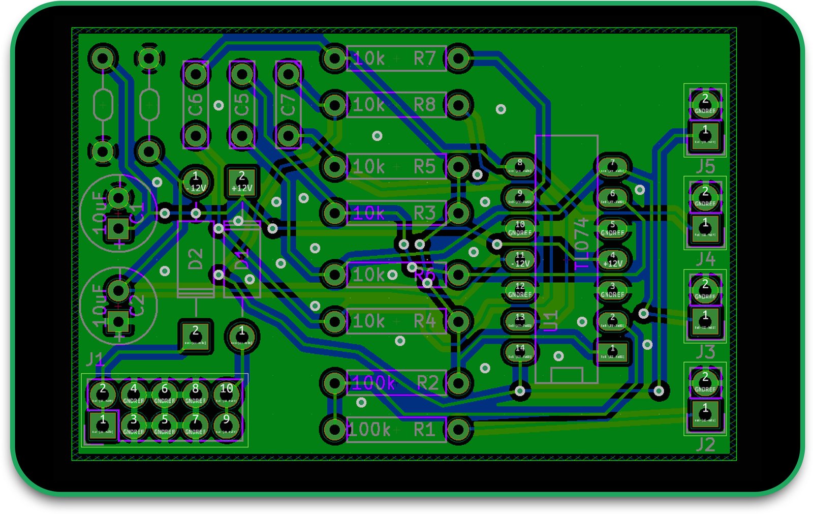
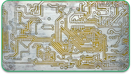
As electronic devices become more compact, robust and sophisticated, so too does the underlying circuitry. This includes the use of High Density Interconnect (HDI) technology that allows miniaturization of the components on a single PCB. Trouble is high complexity and comes with added intricacy in fault finding on circuit boards. Malfunctioning PCB defects can disrupt the entire system, which makes precise diagnosis fast, reliable, and essential.

Circuit board diagnostics is the domain of technicians and engineers, though even hobbyists will do well to understand the basic concepts of PCBs. This article focuses on the primary tools for board-level diagnostics, testing procedures, and PCB defects analysis for effective troubleshooting.

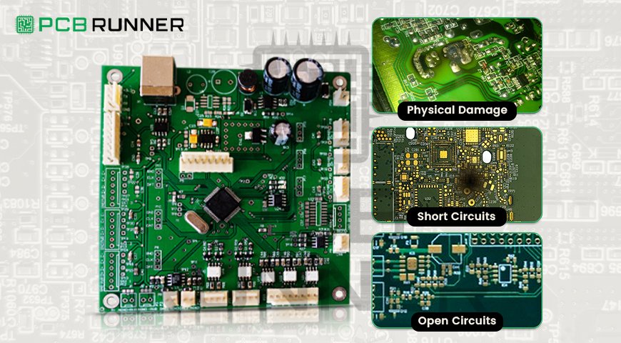
What Are the Most Common Faults with Circuit Boards?

Before getting into the instrumentation and actual testing, it is helpful to put together a hypothesis of what could go wrong with circuit boards. Some of the most common faults with PCBs can be:

Physical Damage

  • Due to excessive temperature: cracked traces, broken solder joints, and burnt components.
  • Damage from dropping or rough handling of the board
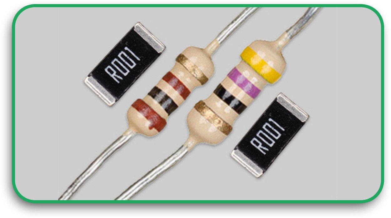
Physical Damage

Component Failure

  • Passive components like resistors, capacitors, and even integrated circuits (ICs) can fail due to overheating.
  • Used-up aging components that deteriorate over time.

Short Circuits

  • Solder bridging or cluttered debris accidentally shorting traces may lead to faults Incorporated shorts within an HDI PCB.

Short Circuit

Open Circuits

  • Open circuits are defined as broken traces or open vias that stop electrical flow.
  • Cold solder joints can create intermittent problems.

Open Circuit

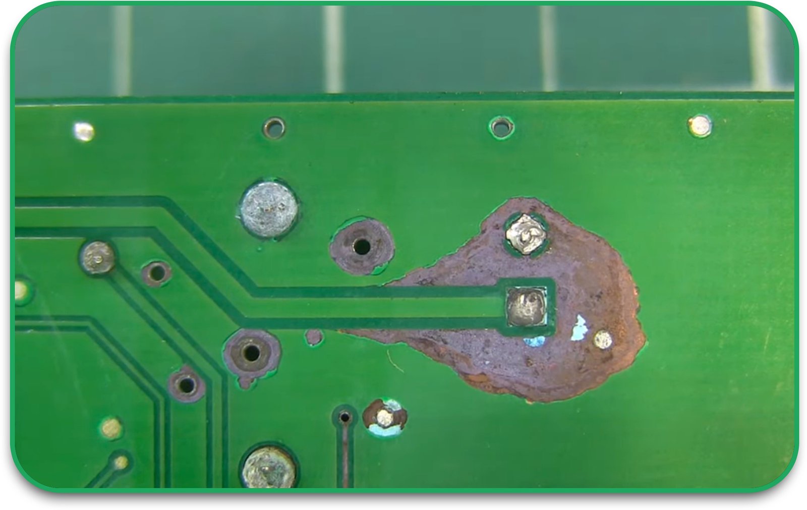
Environmental Factors (Outside Influences)

  • Moisture-related corrosion.
  • Dust, grease, or chemical contamination can impact a manufacturer’s quality control.

Essential Tools for Testing PCBs

In order to identify a fault in the circuit board, specialists use advanced diagnostic tools specific to the task. The following are essential tools for the job.

Multimeter

A Multimeter can help measure and check for bare traces of issues on a circuit board. A Multimeter can be used to measure:

Voltage: Ensures all components are receiving power.

Resistance: Determines if there are broken traces or open circuits.

Continuity: Checks if electrical paths are intact.

Oscilloscope

  • Allows users to view waveforms and check for irregularities in signals.
  • Positive when troubleshooting high-frequency circuits in high-density interconnect PCBs.

Logic Analyzer

Best for testing digital circuits and communication protocols.

Finds logic errors in microcontrollers and memory chips.

Thermal Imaging Camera

  • Shows which parts are overheating and so may have a fault.
  • Can find short circuits without having to touch the device.

Signal Generators

  • Provides specific control test signals to determine if the circuit is responsive.
  • Beneficial when dealing with problems in RF and analog circuits.

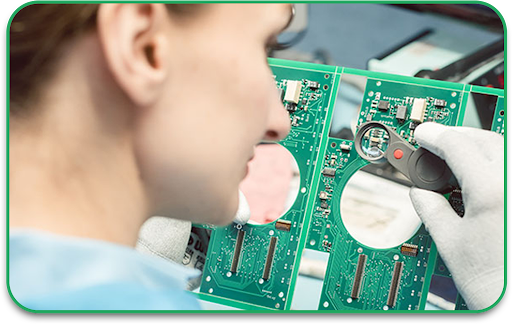
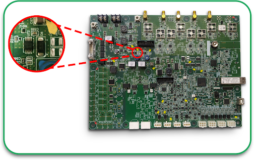
Magnifying Glass or Microscope

Assists in detecting problems with a circuit board like lousy solder joints as well as micro-cracks and corrosion.

Step-by-Step Guide: How to Check Circuit Board Faults

Step 1: Visual Inspection

  • Prior to using any diagnostic tools, perform a thorough examination using your eyes only:
  • Inspect for discoloration or burnt components.
  • Verify any solder joints or ties that may be loose or broken.
  • Examine traces for cracks or components that may be missing.

Step 2: Power Supply Check

  • In case the board does not power on, analyze:
  • The input voltage using a multimeter.
  • Fuses and power regulators for any interrupted connections.
  • Signs of overheating or other damage to power components.

Step 3: Continuity Testing

  • Set the multimeter to continuity mode and check:
  • The connections that link various components.
  • If traces and vias are intact.
  • Learn how to detect PCB flaws with regard to missing connections.

Step 4: Checking for Short Circuits

  • Short circuits can cause the board to fail, so it is essential to check them. Use a multimeter to:
  • Check the resistance that is present between the power lead and the ground wire.
  • Spot areas where excessively high current is being drawn (this indicates a shorted part).
  • Conduct isolation of parts that are suspected to be faulty and remove them for further tests.

Step 5: Component Testing

Some faulty components can lead to failure. Perform the following tests:

Resistors: Use a multimeter to test the resistance.

Capacitors: An ESR meter can be used to identify open and shorted caps.

Diodes: Check the Forward and Reverse Voltage Drops

ICs and Transistors: Use a logic probe or component tester.

Step 6 – Signal tracing with an oscilloscope 

To troubleshoot PCB defects with an oscilloscope, one can:

  • Check the signal’s quality at various stages of the circuit.
  • Check the signal’s shape against the one provided in the datasheet.
  • Some forms of checking for excess noise, glitches, and missing signals.

Step 7 – Functional Testing 

If the components look functional, and the board still fails to work:

  • Start by using a signal generator to insert test signals
  • Keep an eye on the circuit’s behavior using a logic analyzer.
  • If need be, check the functionality of the firmware and software.

Preventing PCB Faults: Best Practices 

To minimize the how to check a circuit board for faults, observe the following: 

Design for Reliability:

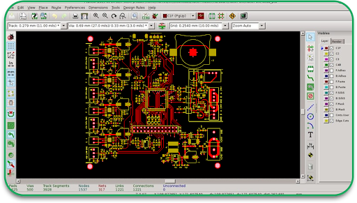
  • Always simulate possible failures with PCB Design Software.
  • Always adhere to the circuit board assembly guidelines and aim for manufacturability.

Quality Components:

  • Always obtain components from reputable PCB circuit board manufacturers.
  • Always stay away from counterfeit electronics and subpar parts.

Soldering Techniques:

  • Ensure good solder joints and clean solder pads.
  • Avoid using too much heat, which may damage components.

Thermal Management:

  • Make use of high-quality thermal heat sinks, vias, and copper pours for heat dispersion.
  • Maintain proper airflow for temperature-sensitive circuits.

Periodic Tests and Checkups

  • Perform error detection at various levels of the circuitry in the printed circuit diagram.
  • In mass manufacturing, make use of automated optical inspection AOI.

Expert Insight

Printed Circuit Boards (PCBs) are becoming more complex due to advanced technology. Identifying and fixing PCB failures is challenging, but even faulty boards can be diagnosed and repaired. Modern PCBs have tiny components, including custom and untestable parts, making troubleshooting difficult. Unlike simple PCBs, they cannot be tested and repaired using standard Automatic Test Equipment (ATE). Fixing these advanced PCBs requires skill and experience rather than just technical knowledge. PCB fault analysis needs strong theoretical understanding and analytical thinking. It is not something you learn only from books but through hands-on experience.

Final Words

Understanding how to check for faults on a circuit board properly is pivotal in the life of an engineer, repair technician, and electronics hobbyist. Failures of printed circuit boards PCBs can be diagnosed accurately using efficient and appropriate circuit board diagnostic devices and tested using appropriate techniques.

Looking for dependable solutions for PCBs?

Get in touch with us for unmatched quality in circuit board assembly as we are PCB Runners, your specialists in PCB circuit board manufacturing.

FAQs

1. What methods of detecting PCB defects are executed using a multimeter?

Devices measuring voltage, resistance, and continuity, like a multimeter, are able to identify all circuit board fault-finding problems, such as open circuits, short circuits, and problematic parts.

2. What are some of the reasons for a circuit board ceasing its function?

Some of the most common ones are failure of components, short-circuiting, broken traces, overheating, and manufacturing flaws.

3. What are some of the best tools for diagnosing PCB defects?

Some of the most essential tools are the multimeter, oscilloscope, thermal camera, logic analyzer, and signal generator.

4. What are some ways to help me avoid PCB failures?

High-quality components, good soldering, thermal management, and adhering to design plans significantly reduce the chances of a PCB failing.

5. Is it possible to fix a broken circuit board?

Definitely, Broken traces can be repaired with wire jumpers, and replacing broken parts will get the PCB working again.

HDI Circuit Design Benefits: Why HDI Flex Circuits Are the Future of PCB Tech

The electronics industry is advancing rapidly, and high-density interconnect (HDI) flex circuits are at the heart of this transformation. These advanced flex and rigid PCB designs are making electronic devices smaller, lighter, and more powerful. From smartphones and wearables to aerospace and medical equipment, HDI flex circuits are shaping the future of technology.

For PCB circuit board manufacturers, keeping up with the latest HDI PCB technology is essential to stay competitive. This blog will discuss what makes HDI flex circuits special, their key benefits, and why they are becoming the new standard for PCB design.


What Are HDI Flex Circuits?

HDI (High-Density Interconnect) flex circuits are a type of printed circuit board with a higher wiring density than traditional PCBs. They combine flexible and rigid PCB sections, allowing them to fit into compact spaces while maintaining strong electrical connections.

Unlike traditional multilayer PCBs, which rely on significant traces and through-hole vias, HDI PCB technology uses microvias, blind vias, and buried vias to create smaller, more efficient circuits.

Key Benefits of HDI Flex Circuits

1. Smaller and Lighter Devices

One of the most significant advantages of HDI circuit design is miniaturization. Because these circuits use microvias and thinner traces, they take up less space. This allows manufacturers to make smaller, lighter devices without sacrificing performance.

2. Improved Electrical Performance

High-density interconnect flex circuits have shorter signal paths, which reduce signal loss and improve transmission speeds. This makes them ideal for high-speed applications, such as 5G networks, aerospace systems, and medical devices.

Why it matters: The shorter the signal path, the less interference and signal degradation you experience. This is crucial for advanced electronics that require precision and reliability.

3. Increased Reliability and Durability

Traditional PCBs can crack or break when exposed to vibration, bending, or extreme temperatures. HDI flex circuits, however, are designed to be more durable.

How?

  • They use flexible materials that can bend without breaking.
  • They reduce the need for connectors and solder joints, which are common failure points.
  • This makes HDI PCB technology perfect for automotive, military, and medical applications, where reliability is critical.

4. Cost Savings in the Long Run

While HDI flex circuits may cost more upfront due to advanced manufacturing processes, they actually save money in the long run.

How?

  • Fewer layers and components mean less material waste.
  • Smaller, more efficient designs reduce assembly and shipping costs.
  • Increased reliability means fewer repairs and replacements.
  • For companies investing in HDI PCB technology, these long-term savings make a big difference.

Why HDI Flex Circuits Are the Future of PCB Tech

As the demand for smaller, faster, and more efficient electronics grows, PCB circuit board manufacturers must adapt. Germany’s HDI market, for example, is rapidly expanding, with industries like automotive, industrial automation, and IoT devices embracing the technology.

Here’s why HDI flex circuits are the future:

  • Smart Devices & Wearables: HDI PCBs enable ultra-thin, lightweight gadgets with high processing power.
  • 5G & High-Speed Data: Faster, more reliable circuits mean better performance in telecommunications and cloud computing.
  • Aerospace & Military Applications: Their durability makes them perfect for harsh environments and mission-critical systems.
  • Medical Innovations: From implants to portable diagnostic tools, HDI flex circuits are improving healthcare technology.

The shift to high-density interconnect flex circuits isn’t just a trend—it’s a necessity for next-gen electronics.

Challenges in HDI Flex Circuit Manufacturing

While the benefits are clear, HDI PCB technology comes with its challenges. PCB circuit board manufacturers need specialized equipment and expertise to produce these advanced boards.

1. Complex Manufacturing Process

  • HDI circuits require precision laser drilling for microvias.
  • Layer stacking and via plating demand high-end fabrication techniques.

2. Higher Initial Costs

  • Advanced materials and processes make HDI flex circuits more expensive upfront.
  • However, the cost savings in reliability and efficiency outweigh these initial costs.

3. Design Considerations

  • PCB routing techniques must be optimized to minimize signal loss and interference.
  • Thermal management is crucial to prevent overheating in compact designs.
  • Despite these challenges, HDI PCB technology is improving every year, making it more accessible to PCB board manufacturers worldwide.

How to Choose the Right HDI Flex Circuit Manufacturer

When selecting a PCB circuit board manufacturer for your HDI flex circuits, consider the following:

  • Experience with HDI Technology – Not all manufacturers have the expertise to handle microvias, blind vias, and high-layer counts.
  • Quality Certifications – Look for ISO, IPC, and industry-standard PCB manufacturing certifications.
  • Customization Capabilities – Ensure they can meet your specific design and material requirements.
  • Testing & Reliability – Advanced testing (such as thermal cycling and impedance testing) is essential for high-performance applications.

A trusted PCB board manufacturer will help you navigate the complexities of HDI PCB technology, ensuring you get a high-quality, reliable product.

Conclusion

HDI flex circuits are revolutionizing the PCB industry, enabling smaller, faster, and more powerful electronics. With benefits like superior performance, increased reliability, and cost savings, they are becoming the go-to solution for next-generation devices.

For PCB circuit board manufacturers, adapting to HDI PCB technology is not just an option; it’s the future. Whether you’re designing smart wearables, medical devices, or high-speed computing systems, investing in high-density, interconnect flex circuits will set your products apart.

Need Reliable HDI PCB Solutions?

At PCB Runners, we specialize in HDI flex circuits and custom-printed circuit boards for a wide range of industries. Contact us today for expert guidance and high-quality PCB solutions!

FAQs

1. What is an HDI Flex Circuit?

An HDI flex circuit is a type of printed circuit board with higher wiring density, allowing for compact, flexible designs with superior electrical performance.

2. Why is HDI PCB Technology Better Than Traditional PCBs?

HDI PCBs use microvias, thinner traces, and advanced materials, resulting in smaller, faster, and more reliable electronic devices.

3. What Are the Main Applications of HDI Flex Circuits?

They are used in smart devices, medical equipment, aerospace systems, automotive electronics, and 5G infrastructure.

4. Are HDI Flex Circuits Expensive?

While initial costs are higher due to complex manufacturing, long-term savings in reliability and efficiency make them cost-effective.

5. How Can I Find a Reliable HDI PCB Manufacturer?

Look for experience with HDI technology, industry certifications, and advanced testing capabilities to ensure high-quality, reliable PCB production.

PCB Etching

The Ultimate Guide to PCB Etching: Methods, Process, and Comparisons

When it comes to making a printed circuit board (PCB), one of the crucial components is etching. Etching removes unneeded copper from the surface of the board, with only needed conductive pathways left. Without Silicon PCB etching, circuits will be non-functional, and their dependability will be at risk. 

For manufacturers, picking the right etching method defines the cost, durability, and performance of the board. Understanding these principles is essential whether you are designing a high-density interconnect (HDI) PCB, a very basic multilayer PCB, or even a prototype. 

The various methods used to etch PCBs will be explained and compared in detail in this blog, helping you to determine the most useful method for your manufacturing needs. 

What is PCB Etching? 

Etching is part of the PCB manufacturing process, where copper is removed from the surface of a PCB circuit board, creating the appropriate traces made of the conducting material. This step occurs only if a resistance layer (a layer that covers the PCB) has already been placed on the board. The copper that was not protected by the resist layer will be removed by the etched solution, leaving the intended paths for the circuitry. 

Etching must be done with accuracy as unregulated etching can lead to over-etching, undercutting, or a non-uniform width of the trace, all of which affect circuit performance negatively. 

Step-by-Step PCB Etching Process 

Preparing the PCB

  • At the start of the etching process first stage of etching is to clean the copper-clad board of any oil or oxidation.
  • This helps with the adhesion of the protective layer, much as a 10-second adhesive will make adhesion for the protective layer easier.

Preparing the PCB

Application of the Resist Layer

The next stage involves shielding the whole board with a protective photoresist, which can be liquid resist or dry film resist. It covers some surface of the shielded copper so as to create the desired circuit design.

Application of the Resist Layer

Circuit Pattern Exposure

The circuit pattern is printed onto the board using a laser imaging technique or a UV light source. The unprotected areas of the shielded copper are left exposed for etching.

Circuit Pattern Exposure_

Etching Method Selection

At this stage, some of the copper that had been shielded is taken away with one of the copper PCB etching processes. The most suitable one varies depending on the complexity and costs of the board alongside the accuracy that is needed. 

Etching Method Selection

Clean the Board and Strip the Resist 

After the etching process, the passive photoresist that is left over is stripped away, exposing the copper traces to view. The last process is to clean the circuit board from any materials it has left. 

Post Assessment Quality Control

The PCB circuit board manufacturer inspects the fabricated board for precision in relation to the specifications individually set, checking that there is no excessive etching or lack of expected traces.

Post Assessment Quality Control

Etching Method Varieties for PCB

Chemical Etching Wet Method

Dissolving copper by use of liquid chemicals is the most usual technique used in PCB fabrication and hence, is ths most used method for PCB fabrication. 

Common Solutions for Wet Etching: 

  • Ferric Chloride (FeCl3): Widely used option due to its low price, but it needs the proper disposal of waste.
  • Ammonium Persulfate: Cuts edges cleaner, ideal for fine-line circuits.  
  • Alkaline Etching (Ammonia Based): Used for High-Density InterConnect (HDI) PCBs because of high accuracy.  

Wet Etching Pros:  

  • Monetary efficiency for bulk production.  
  • Applicable for multilayer and single-layer PCBs.  
  • Simple to execute in basic PCB shops.  

Wet Etching Cons:  

  • Possibility of undercutting (chemicals spreading beneath the resist).  
  • Needs special treatment for waste disposal.  
  • It’s not as accurate as dry etching for advanced circuits.  

Dry Etching (Plasma or Ion Etching)  

Copper is removed by plasma or ion beams with dry chemicals instead of liquids. It is accurate and is often applied to HDI PCB technology. 

Common Dry Etching Techniques:  

  • Plasma Etching: Dismantles copper with reactive gases without harming tiny features.  
  • Ion Beam Etching: Physically removes copper with a focused ion beam for extreme precision.  

Pros of Dry Etching:  

  • Great for accuracy-required processes, such as HDI PCBs.  
  • No possibility of chemical undercutting.  
  • Environmentally safe (no liquid waste to dispose of).  

Cons of Dry Etching:  

  • Equipment and processing are costly.  
  • It’s not as fast as wet etching for large quantities.  
  • It is not commonly found in smaller PCB shops.  

Comparing PCB Etching Methods: Wet vs. Dry Etching

Feature Wet Etching Dry Etching
Cost Lower Higher
Precision Moderate High
Environmental Impact Requires chemical disposal More eco-friendly
Best for Multilayer PCBs HDI PCBs and fine traces
Processing Speed Faster Slower

For most pcb circuit board manufacturers, wet etching is the preferred method due to its cost-effectiveness. However, if you’re working with HDI flex circuits or ultra-fine traces, dry etching may be the better choice.

Challenges in PCB Etching and How to Avoid Them  

  1. Undercutting (Loss of Trace Width)  

 Issue: More copper is removed than desired because chemicals flow underneath the resist layer.  

Solution: For better control, use plasma etching.  

  1. Over-etching (Excessive Copper Removal)  

Issue: Missing traces due to severe over-etching.  

Solution: Never loosen up on monitoring etching time and the strength of the solution.  

  1. Inconsistent Etching (Uneven Copper Removal)  

Issue: Remove copper with varying thicknesses to form a circuit.  

Solution: There should be uniform exposure at the essence of controlled etching baths and some level of abrasive methods.  

  1. Environmental Issues  

Issue: Damage caused to the atmosphere due to inaccurate elimination of etched chemicals.  

Solution: Move towards dry etching or safe chemical disposal methods.  

Etching for High-Density Interconnect (HDI) and Multilayer PCBs.   

Wet etching is typically most preferred for PCBs due to the cost-efficient method, but pours it to these boards; these boards are also a more layered, more power-packed version of traditional boards. Conventional wet etching is inefficient for aimless etching due to fragile lines, micro vias, and multilayers as well.

Plasma etching is regarded as the most preferable option because of its incredible capability to etch intricate details. 

Signal integrity for multilayer PCBs demands etching consistency between layers. PCB etching services usually employ a combination of wet etching for large areas and dry etching for fine-line circuits. 

Expert Insight 

Etching is a technique of PCB fabrication where copper is removed from a laminated board using a defined acid due to the negative image printed over copper. If done manually, it is time-intensive, does not scale well for large board sets, and can get very dirty. Moreover, some of the etching solvents can also be harmful to the user’s well-being. 

Machines have better precision and speed when it comes to etching, and they can simultaneously process many boards in a row; however, for many small PCB manufacturers, they are still too expensive. To solve this, automated etching systems offer a safe and simple method for carrying out the etching sequence with minimum user interaction. 

A PCB serves the purpose of supporting and electrically connecting various components with conductive tracks, pads, and outlined shapes made of copper foil which is affixed to a dielectric substance. This eliminates user error and provides manufacturers with low-cost solutions during PCB etching. 

Future of PCB Etching Technology 

With more complex designs, modern PCBs and their etching technologies are changing. The following list is some trends to monitor:

Ultra-Precise PCBs Flex and rigid etched geometries are best achieved through laser etching. Eco-Friendly Solutions Etching chemicals used in PCB manufacturing are becoming less hazardous. Automated Systems AI etching machines enhance quality and lower error rates.

Conclusion 

The PCB etching process is a fundamental step in PCB fabrication, directly impacting the quality and reliability of circuit boards. Whether you choose wet etching for cost efficiency or dry etching for precision, selecting the right PCB etching method ensures optimal performance for your application.

For high-density interconnect (HDI) PCBs, dry etching techniques provide superior results, while multilayer PCB manufacturers often rely on controlled wet etching for cost-effective production.

Looking for a trusted PCB manufacturer with advanced etching capabilities? Contact PCB Runners today for expert guidance and high-quality PCB fabrication services!

SMD PCB

A Comprehensive Guide to SMD PCB Manufacturing and Design

Surface Mount Device (SMD) technology has changed the design and assembly of modern printed circuit boards (PCBs) the are designed and manufactured. Compared with conventional components that are assembled by means of a hole, SMD circuit boards are more superior and efficient because they save space unlike their predecessor’s left components. This makes SMD circuit boards most suitable for compact and high-performance electronic devices.

SMD PCB manufacturing is important to know especially if you are dealing with a pcb circuit board manufacturer or you are designing your own multilayer printed circuit board. This guide discusses how SMD boards function, details the steps in SMD PCB manufacturing and provides suggestions on how to design SMD PCBs properly using PCB design software.


What is an SMD PCB?

An SMD PCB is a Circuit Board Assembly where Surface Mount Device (SMD) components are used instead of older through-the-hole components. SMD components are soldered on the surface of the PCB, and there is no need to drill any holes.

Advantages of SMD Circuit Boards

Smaller and lighter: Compact designs can be achieved due to SMD components having a smaller footprint.

pcb smd

Higher component density: A more significant number of components can be accommodated within a multilayer printed circuit board.

Faster assembly: Speed in the production process is enhanced due to the automation of SMD PCB manufacturing.

Improved electrical performance: Signals have lower loss and interference due to shorter leads.

Cost-effective: SMD circuit boards can be built cheaply because they are produced at scale.

How SMD Boards Work

PCBs like SMD Boards have some differences from the traditional to, including the use of smaller mountable parts as opposed to through-hole components. These mountable parts can accommodate high frequencies, so they are used in: 

  • Consumer electronics like smartphones, tablets and laptops 
  • Automotive electronics like ECUs and Sensors
  • Medical devices such as wearables and implants 
  • Industrial automation with IoT Sensors and Control units 

In SMD PCBs, signals travel through copper traces, which connect the different electronic components. Resistance to Inductance ration is improved with shorter lead lengths which leads to better circuit performance. 

SMD PCB Manufacturing Process

A high quality SMD circuit board is a result of precision with advanced technology for PCB manufacturing. Following is the SMD PCB manufacturing process: 

Step 1: PCB Design and Prototyping The process starts with an SMD PCB in a PCB design software, which includes Altium, Autodesk Eagle and KiCad. Engineers make sure Components are placed optimally; Signal interference is minimal, and Trace routing Thermal management is done. The final design allows for a prototype to be made so it can be tested.

Step 2: Producing the Printed Circuit Board

In this phase, the layers of the Printed Circuit Board (PCB) are created, which consist of the following processes: 

  • Etching of copper traces on the board  
  • Solder mask application for protective reasons  
  • Component label printing on the silkscreen  

Step 3: Automated Application of Solder Paste

Solder paste is deposited on the pads fitted with a stencil to secure where the components are going to be mounted. The paste contains a mix of tin, silver, and copper in order to provide strong electrical connections. 

Step 4: Use of the Pick and Place Machine

Precision mounting of surface mount devices (SMD) components onto the printed circuit is done by rapid robotic arms. This process is automated, which gaurantees precision and effectiveness which leads to proper mass production. 

Step 5: Solder Reflow

After mounting, the PCB assembled undergoes solder reflow. It is when the PCB assembled is heated in a refractable oven, which liquefies the solder paste to secure the components in the proper position. By controlling the temperature appropriately to prevent overheating, excessive damage to the delicate SMD components can be avoided. 

Step 6: Evaluation and Analysis 

The quality control tests that PCB undergo after assembly involve these three phases:  

  • Automated Optical Inspection (AOI): Analysis and recognition of visible defects in soldering as well as(device misalignment) 
  • X-Ray inspection: Determine the solder joints concealed beneath components like Ball Grid Arrays (BGAs)  
  • Functional Testing: Ensures that proper circuit performance occurs before final assembly.  

Step 7: Wrap-Up of Assembly and Product Distribution 

Post-test, the assembled Surface Mount Device(SMD) circuit boards are incorporated into the final product, put into a package and forwarded to the customer.

How to Design SMD PCBs – A Guide

When designing SMD circuit boards, best practices are followed for optimal performance and board reliability. Here is a step-by-step breakdown of how to design SMD PCBs 

Choose the Correct PCB Layout 

Software Printed circuit board design software is used to construct the PCB layout. Some of the most common include: – Altium Designer- Best suited for specialized designs – KiCad- Open-source version is handy for beginners – Eagle – Commonly used for both industrial and hobbyist PCBs 

Improve the Component Placement 

Ensure that high-frequency components are placed together to reduce signal loss. Sensitive circuits should be placed further away from heat-generating components. Separately position power and ground planes to maintain stability. 

Create a Designed Trace Routing 

Draw direct traces without reducing resistance. Ensure uniform current flow by maintaining consistency in trace widths. Signal reflection is prevented by avoiding 90-degree angles in traces. 

Manage Thermal Control 

Invest in thermal vias close to power components. Increased dissipation of heat is accomplished by using heat sinks or copper pours. 

Choose Correct Solder Mask 

Solder mask protects PCB from oxidation and solder bridging. Do a PCB circuit board manufacturer search and select one that uses high-quality solder masks to ensure durability.

SMD PCB vs. Through-Hole PCB: Which One is Better?

While SMD circuit boards dominate modern electronics, through-hole PCBs still have some advantages. Let’s compare them:

Feature SMD PCB Through-Hole PCB
Component Size Smaller, compact Larger, bulkier
Assembly Speed Fast (automated) Slow (manual or wave soldering)
Mechanical Strength Less durable Stronger for high-stress environments
Cost Lower for mass production Higher due to manual labor
Signal Performance Better for high-frequency circuits More resistance and interference

For most applications, SMD PCBs offer better performance, lower cost, and faster production. However, through-hole technology is still used for high-power and high-reliability applications like aerospace and military systems.

Essential Considerations When Selecting a PCB Manufacturer for SMD Boards

Finding a reliable PCB manufacturer is the first step in getting quality SMD circuit boards. Consider the following: 

Manufacturing Capabilities 

  • Can they manufacture multilayer printed circuit boards? 
  • Can they execute High-Density Interconnect (HDI) technology? 
  • What are the quality standards that they practice? 

Prototyping Services 

  • Do they provide rapid turnaround prototypes for pre-production testing? 
  • Are they able to produce both small and large-volume orders? 

Quality Control 

  • Do they use Automated Optical Inspection (AOI) X-ray and Functional Testing? 
  • Do they comply with ISO and IPC quality standards? 

Customer Service 

  • Do they respond promptly to redesign requests? 
  • Do they provide DFM (Design for Manufacturing) services? 

With PCB Runners, you get SMD PCB manufacturing services and impeccable quality circuit board assembly for all types of businesses around the globe. From developing prototypes to mass production, we provide dependable, low-cost options. 

Expert Insights

Surface Mount Technology (SMT) has transformed the electronics industry by making devices smaller, lighter, faster, and more affordable. Unlike older methods, reflow soldering has become the preferred technique because it provides higher efficiency, reliability, and better manufacturing results compared to wave soldering.

To meet the demand for compact and high-performance electronics, area array packages have replaced traditional designs. These packages offer higher input/output (I/O) density, improved manufacturability, and better speed while reducing the overall size of components.

SMT components, known as Surface Mount Components (SMCs), are widely used in electronics. They include capacitors, resistors, transistors, diodes, inductors, integrated circuits (ICs), and connectors. However, due to their small size, most SMCs can only handle power dissipation of 1 to 2 watts.

These components are mounted onto Printed Circuit Boards (PCBs) using different methods like solder paste reflow, wave soldering, or conductive adhesive curing. While conductive adhesives are less common, they are used in flexible circuit boards or for heat-sensitive components. SMT continues to be a key technology in modern electronics manufacturing.

Final Thoughts 

The introduction of SMD circuit boards is constantly changing the electronics industry with smaller, faster, and better devices. Knowing the SMD PCB manufacturing procedure combined with the best methods of how to design SMD PCBs will lead to enhanced performance and reliability.

Searching for a reliable PCB manufacturing company? Look no further; PCB Runners specializes in custom-printed circuit boards and high-precision SMD assembly. Reach out today for expert assistance with PCB fabrication and circuit board SMD assembly. 

Frequently Asked Questions (FAQs)

What is SMD PCB? 

An SMD PCB is a printed circuit board that incorporates surface mount devices in place of traditional through-hole components. 

How does SMD PCB manufacturing work? 

The process comprises fabrication of the PCB, solder paste application, placement of components, reflow soldering, and quality inspection. 

Which software is the most effective to use for designing SMD PCBs? 

The most popular choices would be Altium Designer, KiCad and Eagle. 

What are some benefits of SMD PCBs compared to through-hole PCBs? 

SMD boards are smaller, faster, cost effective and can accommodate greater component density. 

Where can I find quality SMD PCB fabrication? 

For expert SMD PCB fabrication and circuit board assembly, contact us today at PCB Runners.

A Complete Guide to PCB Routing: Design Rules and Best Practices for Success

Effective and efficient planning of PCB routing directly influences the PCB board assembly work. Effective routing ensures optimal signal flow, reduces interference, and improves thermal and overall circuit performance. In all types and levels of PCBs, from single boards and multilayer systems, manufacturers adhere to strict PCB routing policies.
Routing involves planning trace paths, spacing between conductors, and stacking layers in a manner that facilitates the easiest path for signal flow and cooling. Routing issues can deteriorate signal strength, increase EMIs, and reduce overall dependability.

In this article, we will discuss essential PCB routing best practices and rules, sophisticated techniques in PCB fabrication to enhance circuits within designed bounds, and other cutting-edge techniques and technologies.
If you need precise route crafting for your CAD designs, contact PCB Runners and let professionals handle the work.

PCB Routing

What is PCB Routing?

Connecting the different components of a circuit entails routing, which involves placing traces for the electrical pathways that convey the signal and power. These pathways are referred to as traces, and routing techniques can make use of multiple boards, and via placement out of alignment for prevention of crosstalk, noise, and interference that form wires in close proximity to one another.

Cutting-edge PCB design software and automation systems allow modern manufacturers to efficiently optimize complex circuit routing based on performance metrics and ease of manufacture.

PCB Design Guidelines

Trace Width and Spacing

  • Proportions of Trace width for current capacity must be balanced.
  • Reduction of resistive heat and increased thermal output is seen with broader electrical pathways.
  • Standard spacing avoids signal overlapping and cross-wiring.

Trace Width and Spacing

Vias Types and Placement

Different levels of a PCB board can be interconnected with Vias. The common types of Vias are:

  • Through-Hole Vias – These pass through the entire board.
  • Blind Vias – These connect inner layers with outer layers.
  • Buried Vias – These only connect internal layers.

Vias Types and Placement

High-Speed Routing and Signal Integrity

  • To lower signal bounce, sharp angles greater than 45° should be avoided.
  • For the transmission of high-speed data, the routing of differential pairs should be employed.
  • Traces pertaining to the clock and other high-speed signals should be short and direct.

High-Speed Routing and Signal Integrity

Ground and Power Planes

  • The placement of defined ground and power planes minimizes noise and maximizes efficiency.
  • Elimination of interference is encouraged while keeping the planes as continuous as possible.
  • Altering the portion of the ground plane could lead to EMI difficulties.

Ground and Power Planes

Multilayer PCB Stack-up Layers

  • An immediate advantage of using multilayer PCBs is improved routing versatility for densely packed components.
  • Interchange the Power/ground layer with signal layers and vice versa for reduced interference.
  • For mechanical strength, ensure the stack-up layers have symmetry.

Multilayer PCB Stack-up Layers

Best Practices for PCB Routing

Focus on Component Placement

Before beginning to PCB route, make sure to place components appropriately. Try to:

  • Integrate associated components (for example, power circuits and signal paths).
  • Minimize interference by bringing high-frequency components closer together.
  • Provide adequate space for connectors and mounting holes.

Refine Trace Routing

Maintain ease of manufacture and orderliness with your PCB trace routing:

  • Direct routing should be to the point and as short as possible.
  • Glance at the 45° rule. 90° bends are too sharp.
  • Balance spacing between traces that are close to each other to avoid crosstalk.

Don’t Route Over Split Planes

  • Sustain return paths by preventing signals from running over split power or ground planes.
  • Enhance EMI shielding through the use of ground fills and stitching vias.

Thermal Management Issues

  • Use thermal relief pads to disperse heat in high-power designs.
  • Ensure power traces are dispersed evenly to prevent overheating.
  • The use of thermal vias may be considered in order to enhance heat dissipation.

Observe DFM Policies

  • Make sure that traces, vias and pads are within the PCB routing guidelines for manufacturing.
  • Clearances suitable for soldering and assembling must be provided.
  • Prevent routing vias in close proximity to component pads, as this will cause solder wicking.

Advanced Techniques in PCB Routing

Differential Pair Routing

For USB, HDMI, and Ethernet signal routing, the following apply:

  • Use the same trace width and spacing throughout.
  • Pair routes with the same length to maintain signal integrity.

Controlled Impedance Routing

  • Minimizes signal reflections in RF and high-speed digital circuits.
  • Calculation of trace width and spacing needs precision based on board material properties.

Via Stitching for EMI Shielding

  • Placing vias along the signal trace helps reduce EMI.
  • Common in RF and sensitive analog circuit designs.

Length Matching for Synchronized Signals

  • Ensure equal trace lengths for clock signals and data signals so they arrive at the destination at the same time.
  • Use serpentine routing to equalize lengths if needed.

The Role of PCB Manufacturers in Routing Optimization

Manufacturers of PCBs have significant experience, which helps in optimizing routing for PCB board assembly and performance. With the use of sophisticated techniques in the fabrication of PCBs, these manufacturers are able to:

  • Give suggestions about the design with the aim of enhancing the routing.
  • Comply with the rules of PCB routing set for manufacturing.
  • Modify trace layouts designed for speed and power consumption.
  • Fix errors using design rule check (DRC).

Conclusion

Following best practices in PCB routing is essential in achieving optimal performance, reliability, and manufacturability in circuit board design. Engineers can successfully improve trace layouts, reduce crosstalk, and the overall signal integrity through proper trace routing techniques.

Working with a proven and established PCB manufacturer helps maintain compliance with the design rules of the PCB routing which enhances the efficiency of upwards of PCB board assembly and the quality of the end products.

Are you looking for assistance in routing and fabricating advanced PCBs?

For tailored professional solutions in PCB fabrication, routing, and multilayered PCBs, Trust PCB Runners. 

FAQs

What does routing on a PCB mean? 

Routing consists of the placement and layout of the electrical traces that connect various components on the PCB.

What makes important computer-aided manufacturing routing guidelines? 

Routing guidelines assist in maintaining proper signal conveyance, limiting outside signals, and manufacturability.

What are the common PCB routing rules for manufacturing? 

Common routing rules include appropriate solder mask openings, transverse trace clearance, and spacing on traces.

What benefits do multilayer PCBs offer for routing? 

Multilayer PCBs provide better separation between the signal, power, and ground layers, thereby decreasing interference and boosting performance.

What are the best PCB routing techniques for high-speed signals?

For high-speed designs, use differential pair routing, controlled impedance, length matching, and via stitching to maintain signal integrity.

Automated PCB Manufacturing

Automated PCB Manufacturing: The Benefits of Smart Manufacturing for PCBs

Outdated methods of traditional PCB production techniques are unable to keep up with the ever-evolving electronics industry. The industry’s critical needs, such as HDI PCBs and smaller components, are clearly not going to slow down, which is precisely why automated PCB manufacturing techniques need to be implemented.

It is only with the assistance of smart manufacturing technology that PCB manufacturers can reduce costs and improve efficiency, overall quality, and yield. Modern Intermediate and major industry requirements are being met by Smart Systems that are capable of robotic PCB board assembly and using Automated Inspection Systems.

This blog will discuss the procedure of the smart manufacturing process and its features, along with automation implementation advantages that would benefit PCB board manufacturers.

Smart Manufacturing for PCBs: What is it?

The Explanation Behind Automated PCB Manufacturing

Due to its ability to introduce robotics, AI, IoT, and automation into the PCB production area, Smart manufacturing is now a widely used term in the industry. The incorporation of minimum human activity in PCB smart manufacturing significantly decreases errors while maintaining consistency and increased accuracy.

Head Of The Departments In Smart Production Of PCBs:

The Advanced assistance robotics offers are:

  • Smart Assembly of PCB boards by robots with documented proper component placement.
  • Defect Identifying Automated Optical Inspection (AOI) and X-ray scrutinizing.
  • Smart Arrangement of PCBs driven by AI to fit intricately optimized layouts of HDI.
  • Craftsmen by IoT sensors obtain direct supervision of the fabrication of PCB, monitoring the assembly in real-time.

The implementation of smart technology in manufacturing processes for PCBs allows for mass production while preserving quality. This makes it easier for modern PCB assemblers to operate.

Advantages of Smart Manufacturing Technology for PCBs

1. Boosted Productivity

Automated systems accomplish PCB fabrication and assembly, which leads to a faster and more time-efficient manufacturing process. Robots can accurately assemble thousands of boards each hour, which is much greater than the output for manual assembly.

2. Minimized Errors

Automated PCB manufacturing offers performances that surpass the manual processes of soldering and component placement with respect to misalignment and defects. This form of manufacturing guarantees that every board produced meets the stringent quality standards set.

3. Lower Expenses

Smart manufacturing practices lead to a decrease in the cost of labor, material wastage, and even rework expenditures. PCB board manufacturers can manage their resources more efficiently, increasing overall production while enhancing profit margins.

4. Advanced Quality Control

AI-powered inspection systems incorporated into the smart manufacturing processes of PCBs enable the identification of defects in solder joints, the width of traces, and the application of solder mask material.

5. Targeted for High Volume Production Scalability

Smart manufacturing provides greater density interconnect (HDI) PCBs with the capability to complex circuit designs in a very efficient and precise manner. The 

PCB Smart Manufacturing Process

1. Automated Design and Prototyping

The very first step of designing a PCB begins with the Smart systems using AI-powered PCB design software, which takes care of layout optimization for signal integrity and thermal management in addition to optimizing layouts for thermal and signal well-being. Prototypes undergo a DFM check, which must be passed before fabrication to ensure all designs are compliant.

2. High-Precision PCB Fabrication

The steps involved in the automated fabrication of PCBs include:

  • Drilling vias and component holes using laser precision-equipped drilling.
  • Stacks of multilayer PCBs are handled automatically.
  • Laminating High-Density Interconnection PCBs with advanced techniques.

3. Solder Mask Application & Component Placement

Using automated spray coating to apply solder masks improves CASS longevity by keeping traces from oxidation as well as contamination. Pick and place robots also enable mounting components on the board with micron accuracy.

4. Automated Soldering & Reflow Process

  • Performs AI-controlled reflow soldering, which automates temperature profiling for perfect solder joints.
  • Wave soldering for through-hole components to eliminate manual errors.

5. Smart PCB Testing & Quality Assurance

Smart AI Automated Optical Inspection (AOI) and X-Ray Inspection identifies defects not untrained eyes can identify. Evaluation of functional parameters is also done to ensure the performance level of the PCBs before shipment.

6. Data-Driven Process Optimization

Real-time data collection of the production via IoT sensors is an intelligence offered by smart factories. Such data helps in enhancing process efficiency and reduction of waste as well as improving yield rates.

Problems with Smart PCB Manufacturing

1. High Initial Investment Costs

Automated PCB manufacturing requires sophisticated equipment like advanced robotics, AI software, and advanced machinery. These additions are quite expensive.

2. Skilled Workforce Requirement

Although automation reduces the need for manual work, smart manufacturing systems still require trained engineers to operate and maintain them.

3. Integration with Pre-Existing Systems

Smart technology can’t be implemented into legacy PCB manufacturing setups at once, which makes integration with modern-day technology challenging.

Developing Trends in Automated PCB Manufacturing

1. AI-Driven PCB Design & Routing

Intelligent systems help automate the routing of PCBs and aid in attaining the proper placement of components so that there is no signal disruption.

2. 3D-Printed PCBs

Additive manufacturing is on track for developing materials that can yield 3D-printed circuit boards. Such technology can drastically cut down on the use of materials required to design PCBs.

Production of PCBs has been getting a bad reputation and is viewed as wasteful. Due to eco-friendly initiatives rising in popularity, there is a shift towards sustainable processes when it comes to manufacturing PCBs by focusing more on recyclable materials and energy-efficient processes.

3. Blockchain in PCB Manufacturing

With the implementation of Blockchain technology, tracking PCBs throughout the supply chain becomes easier and prevents counterfeiting without hiding sensitive information. This makes the process of tracking components more reliable.

How to Opt for a Manufacturer That Best Suits Your Needs for Smart Manufacturing PCB

Make sure to point out the expertise of the smart PCB producers to guarantee high level automation done by AI inspections and integration of HDI PCBs.

1. Certifications & Compliance

Verify ISO 9001 or ISO 14001 certifications and ensure the IPC standards are adhered to by the manufacturer.

2. Production Flexibility

A dependable PCB assembler should be able to manage small-batch prototypes as well as high-volume production.

3. Data-Driven Approaches to Manufacturing

Predictive maintenance, real-time analytics, AI optimizations, and other advanced analytic tools are leveraged by the leading PCB manufacturers.

Final Thoughts

The adoption of smart technology in the manufacturing process of PCBs has revolutionized the electronics industry by accelerating reliability and affordability in the production of PCBs. Automated manufacturing of PCBs greatly reduces costs while improving precision and scalability.

At PCB Runners, we offer interconnect PCBs alongside advanced automation and AI quality control. We are the leaders in smart PCB production systems.

Looking for a Smart PCB Manufacturing Partner?

For the latest solutions in PCB fabrication and assembly, get in touch with PCB Runners today!

FAQs

1. What is Smart Manufacturing for PCBs?

Smart manufacturing applies AI, automation, robotics, and IoT technologies to the production of PCBs to enhance efficiency and minimize errors while improving overall quality.

2. What are the Benefits of automated PCB manufacturing?

  • Shorter production cycles
  • Increased efficiency and productivity
  • Lower operational costs
  • Enhanced mass production scalability

3. Do all PCB manufacturers use smart manufacturing?

Most PCB board manufacturers have not fully automated their processes, but a significant number are moving toward AI automation and automated quality control systems.

4. What is the future outlook for PCB manufacturing?

The future includes 3D-printed PCBs, AI-controlled routing, blockchain-based traceability, and eco-friendly production.

PCB Failure

Common Reasons for PCB Failure and How to Avoid Them

The failure of PCBs is costly and, if not handled properly, can compromise the entire system. In many ways, the printed circuit board acts like the spine of any electronic device. It ensures inter-component communication and coordination is smooth.

Most custom-printed circuit boards undergo extensive engineering design but can still experience functional failures, inefficiencies, complete breakdowns, and system malfunctions. Addressing and understanding the root cause of PCB failure is essential to assist engineers and printed circuit board manufacturers in strengthening assembly and design improvements.

Poor design, unsatisfactory manufacturing, degradation of materials, or environmental conditions can all lead to PCB failure. Timely diagnosing problems with a board’s functionality using effective PCB failure analysis strategies can reduce product failure risks, loss of resources, and time.

This blog will discuss the most effective practices on how to prevent PCB failure, conduct a thorough failure analysis, and identify primary causes that contribute to the failure of printed circuit boards.

Are you on the lookout for failure-resistant, high-quality PCBs? Feel free to get in touch with PCB Runners whenever you need expert consultation for circuit board manufacturing solutions.

What Causes PCB Failure?

PCBs may fail due to several reasons, such as the design of the board, material selection, manufacturing defects, and the surrounding environment. Below are some of the most common reasons for PCB failure:

A Poor Design of the PCB

  • Every trace width is designed with the goal of being as narrow as possible, leading to overheating.
  • Components are placed in a way that creates interference, which is not the intended purpose.
  • Thermal relief systems are lacking in structures to prevent heat containment.
  • Conductive paths are too close together to allow for short-circuit bypass.

A Poor Design of the PCB

Manufacturing Issues

  • Soldering Problems – Cold joints, bridging, and excess or insufficient soldering may lead to failures in a particular connection.
  • Delaminations – Separation of the levels of a PCB as a result of poor lamination.
  • Via Problems – Not plating or drilling alignment affecting the electric link.
  • Copper Trace Damage – Weak tracing snapping from forces.

Manufacturing Issues

Stress Factors and Aging

  • High amounts of heat and humidity can burst the material, leading to failure.
  • Movement and shaking – repeated physical stress leads to weakened joints.
  • Corrosion- Damage from moisture and chemicals degrades conductive materials.
  • Electrostatic Discharge (ESD) – Dangers for circuits and components.

Overstraining Electricity (EOS) and Power Problems

Suffering damage from overvoltage or excessive current. Inadequate grounding leads to havoc and false command behavior within the circuits. Damage resulting from reversing polarity connections to the parts of the PCB.

1. Contamination & Impurities

  • Chemical contaminants and dust can disrupt circuit performance due to the presence of flux residues.
  • Corrosion and oxidation are a result of poor post-cleaning practices after manufacturing.

2. PCB Failure Analysis Techniques

Upon failure, each printed circuit board is analyzed with specific techniques aimed at reasoning for the failure and what rectifications need to be done. The most common approaches are:

3. Visual Inspection

Look for signs like broken traces, misaligned components, burnt areas, and discoloration.

4. X-ray Inspection

For inspection of connections on multilayer printed circuit boards, solder joints, and vis, X-ray machines are employed.

5. Thermal Imaging

Thermal Imaging is used for locating overheating parts, hotspots, and areas of weak thermal control.

6. Electrical Testing

Continuity Testing: Checking connections to ensure there are not any breaks in them.

Functional Testing: Ensuring that the PCB provides the expected operation.

In-Circuit Testing (ICT) – Testing on the components and their interconnections.

7. Scanning Electron Microscopy (SEM)

SEM is used for capturing detailed images aimed at identifying cracks, delamination, and other micro-defects embedded in the materials of the PCB.

8. Analyzing Solder Joints

Feedback from bridging, modifying poor refusals, and cold solder joints should be confirmed in solder joint verifications.

Prevention of Failures in PCBs

To enhance the reliability and durability of a printed circuit board, the following failure prevention techniques should be employed.

1. Design for Reliability

  • Increased reliability starts with using proper routing and thermal management of the board’s traces on PCB design software.
  • DFM or Design for Manufacturing guidelines have to be followed so that the assembly process is free of assembly defects.
  • Trace width and space allowance must be sufficient to avoid overheating.

2. Choose High-Quality Materials

  • Choose a PCB circuit board manufacturer that uses quality substrate materials.
  • For multilayer printed circuit boards, use multilayered boards for more complex designs that require more durability.
  • Use materials that are more resistant to heat, like FR4 and polyimide, or even ceramic substrates, for better longevity.

Improve PCB Manufacturing & Assembly Processes

Work with other trusted PCB circuit board manufacturers to ensure strict quality control standards are being followed.

  • Check for proper solder mask application that could lead to oxidation and contamination.
  • Use automated optical inspection (AOI) to check for defects before the end of production.

Enhance Thermal Management

  • Use thermal vias and heat sinks to dissipate heat from high-powered components.
  • Position temperature-controlling components near the heat-generating components.
  • Use thermal relief pads to avoid the build-up of critical excessive heat in sensitive areas.

1. Protect Against Environmental Damage

  • Deny moisture protection can be applied by conformal coat coverings alongside chemical and dust shielding.
  • Prevention against oxidation for contact nodes can be done using gold or silver plating.
  • If the PCB is in harsh conditions, protect the design for IP-rated enclosures.

2. Prevent Electrical Failures

  • Remove the possibility of electromagnetic interference (EMI) through good grounding and shielding implementation.
  • Innumerous fuses, varistors, and even TVS are diodes designed for overvoltage protection.
  • Avoid voltage changes by making sure the power supply circuit is intact and validated.

3. Conduct Rigorous Testing and Ensure Quality Control

  • Perform functional, burn-in, and reliability testing prior to commencing mass production.
  • Multilayer PCBs with internal layers require X-ray inspection and ultrasonic testing for hidden defects.
  • Quality standards for PCB fabrication set forth by IPC-A-600 and IPC-6012 are mandatory.

Future Trends in PCB Reliability & Failure Prevention

The evolution of the electronics industry is shifting the focus towards newer technologies for preventing failures in PCBs during manufacturing. Emerging trends include:

1. AI-Based PCB Design and Testing

Before the manufacturing stage, AI algorithms can aid in identifying potential design flaws.

Early detection of potential failures is now possible through machine-learning-based predictive maintenance.

2. Advanced PCB Materials

The development of flexible PCBs includes self-healing capabilities.

Graphene-based PCBs are being adopted due to their high conductivity and the ability to dissipate heat efficiently.

3. 3D Printed PCBs

Custom custom-made precise PCBs can now be readily designed.

Enhanced rapid prototyping capabilities and reduced material waste have been achieved.

4. Improved Conformal Coatings

Moisture and contamination-resistant nano coatings offer better protection.

Durability is improved with faster production by using UV-curable coatings.

Manufacturers are able to build PCBs with lower failure rates by increasing their resilience to harsh operating conditions through newly invented innovations in PCBs.

Conclusion

Diagnosing the faults and understanding the reasons behind a PCB failure help in improving its reliability. This could be caused by a design error, environmental factors, excessive electrical loading, or selection of substandard materials, but all can be worked on to ensure effective PCBs remain durable.

At PCB Runners, we take pride in providing preeminent custom printed circuit boards as per industrial requirements, which ensures the best performance and tailoring of failure avoidance techniques in each application.

High-quality PCBs are custom-made for your specific needs. We offer multilayered PCBs paired with refined failure analysis, making a trusted source for all your requirements. Contact Us now to discuss your projects further.

Frequently Asked Questions (FAQs)

1. What usually causes the failure of circuit boards?

Factors such as an overloaded power supply, overheating and external stress, unsatisfactory design and manufacturing, as well as contamination tend to cause the most faults.

2. What are proposing capturing techniques for circuit failure?

The use of high-grade materials, proper management of thermal load, functional testing, and ample design modifications are bound to oppress failure.

3. How is the failure of a PCB diagnosed, and why is it essential?

Diagnosing issues to enhance dependability by means of visual inspection, electrical tests, x-ray examination, and material analysis constitutes failure analysis.

4. How does environmental stress affect the performance of a PCB?

Factors such as humidity, heat, vibration, and corrosive chemicals cause degradation of the insides of a PCB, leading to oxidation, cracks, or joint soldering failure.

5. Why are multilayer PCBs considered superior to their single-layer counterparts?

High-performance electronics require superior durability, signal integrity, and improved heat dissipation, a feature provided by multilayer PCBs.

PCB Manufacturing Methods: Key Techniques and Innovations for Circuit Boards

Even your smartphone and laptop make use of a PCB (Printed Circuit Board). Circuit boards are essential in electronics, providing a platform for all components as well as ensuring the devices operate effectively. But have you ever asked yourself the question: how were those boards manufactured?

The PCB manufacturing process is complicated and consists of several phases, from conceptual design to final evaluation. Knowing these processes can help professionals make better choices, be it an engineer, hobbyist, or even an establishment seeking a trustworthy PCB board manufacturer.

This blog will provide everything from seeking information on the newest industry advancements and innovations to what PCB fabrication is. We will also disentangle the steps that explain how to fabricate PCB, as well as cover the sophisticated technologies high-density interconnect PCB manufacturers employ to produce next-gen circuit boards.


high-speed circuits qre future of PCB manufacturing

What is PCB Fabrication?

Through fab processes, designers can break down their schematic into portions; fabrication can be defined as the step of transforming a design into an actual physical circuit board. It includes the laying out of the copper traces, drilling the relevant holes, and putting protective layers before the components are put together.

The PCB Manufacturing Process

1. PCB Design and Layout

Before any construction can start, soldering components to a PCB requires a basic layout to have been previously done in CAD or CAM PCB design software. This defines the location of electrical elements and connecting wires.

2. Material Selection

The following step is a selection of appropriate PCB board material. Some of the more important options are: 

Fibreglass Reinforced Epoxy FR-4: Used as the base standard for most boards.

Metal Core: Used for LED lighting as well as power electronics because they dissipate heat.

Polyimide: Used for flexible PCBs due to its flexibility and capability to withstand high temperatures.

3. Printing the Circuit Design

The design is printed on the board with a photoresist technique that engraves the design into the copper covering the board.

Advances in PCB manufacturing


4. Etching Process

Etching is the process used to remove the extra copper while retaining the etched paths. This can be done in two primary manners:

Wet Chemical Etching: Uses acid solutions to get rid of any unwanted copper.

Dry Etching: More accurate material removal is done by the use of lasers or plasma.

Innovations in PCB manufacturing

5. Drilling Holes

Holes are drilled on the multilayer boards to facilitate interlayer connections and to mount surface-mounted components. To make microvias in high-density interconnect PCBs laser drilling is used which significantly improves signal performance.


Drilling holes is a critical step in PCB manufacturing

6. Plating and Copper Deposition

To create electrical connections between the layers, copper is plated onto the holes. This step is done after drilling.

 PCB making methods

7. Solder Mask and Silkscreen Application 

A silkscreen layer provides a way to label components, while a solder mask layer is meant to protect copper traces from oxidation and short circuits. 

8. Surface Finishing

There are various surface finishes added on a PCB to improve the durability and solderability of the PCB, such as: 

HASL (Hot Air Solder Leveling) – very cheap but not very durable, so its lifespan is short. 

ENIG (Electroless Nickel Immersion Gold) – is used for high-reliability applications, which is very common. 

Immersion Silver/Tin – available for other specialized needs.

9. Quality Control and Testing

These boards go through numerous testing procedures to guarantee quality before shipping, for example: 

Automated Optical Inspection (AOI): checks the board for defects visually. 

X-ray Inspection: determines whether or not there are any issues with the hidden layers of the board. 

Electrical Testing: checks to see if the circuitry within the board works.


The manufacturers must comply with strict industry standards and regulations.

10. Final PCB Assembly

When the board passes the testing phase, the components are then soldered onto the board utilizing: 

Surface Mount Technology (SMT) – common with modern electronics devices. 

Through-hole technology (THT) – is used in industrial electronics because it’s more durable.

Sustainable practices are becoming more important in circuit board assembly process.


Key PCB Manufacturing Methods

1. Traditional Etching (Subtractive Process)

Best For:PCBs that are either single-layer or double-layer of standard forms. 

Pros: Cheap and reliable, so a lot of people make use of it. 

Cons: Not highly precise hence difficult for high-concentration designs.

2. Additive Manufacturing (3D-Printed PCBs)

Best for: Custom designs and prototypes

Pros: Short lead times and Produce little scrap material.  

Cons: Not well suited for large quantity production. 

3. HDI PCBs – High-Density Interconnect PCBs

Best for: Electronics requiring high performance in small devices.    

Pros: Smaller devices can be made while increasing signal quality.    

Cons: Increased unit manufacturing cost. 

4. Rigid-Flex and Flexible PCBs

Best for: Wearable devices, Automotive, Aerospace.    

Pros: Durable and lightweight.  

Cons: Special handling and materials needed.   

5. MCPCB – Metal Core PCBs

Best for: Devices that require a lot of power, such as LEDs and power supplies.    

Pros: Outstanding heat dissipation.  

Cons: More weight than other PCBs.  

Innovations in PCB Manufacturing   

1. AI-enhanced PCB Design:

The use of machine learning assists in optimizing circuit layouts by reducing defects while increasing efficiency.   

2. Laser Drilling for HDI PCBs:

A laser’s use of ultra-small vias allows for high-speed and compact PCBs.   

3. Eco-Friendly PCB Manufacturing:

New techniques use water-based etching combined with lead-free soldering, reducing pollution. 

4. Hybrid PCBs:

Combining rigid and flexible layers results in more durable and better-performing advanced electronics.  

Choosing the Right PCB Manufacturer

1. Years of Operation and Industry Experience

Seek a PCB board manufacturer that has worked with your industry, whether it be consumer electronics, medical technology or aerospace.   

2. Manufacturing Capabilities

Choose from PC board manufacturers that are able to do HDI, multilayer, and flex PCB fabrication.

3. Certifications and Quality Standards

A good PCB manufacturer must obtain the following:

  • ISO 9001 certification for Quality Management.
  • Compliance with IPC Standards for reliability of boards.
  • Compliance with RoHS standards for environmentally friendly manufacturing.

4. Costs and Speed of Production

Analyze costs and lead times to determine the best value for your work.

5. Customer Support

A competent PCB manufacturer should offer responsive technical and design support.

Future Trends in PCB Manufacturing 

PCBs design and manufacturing is expected to change with the onset of new technologies. Some of the changes you may want to monitor include:  

  • PCBs are designed for 5G and IoT connectivity. 
  • PCBs are made with nanotechnology for super slim, lightweight, and high-performing boards.
  • Smart factories with automated systems will improve the speed and accuracy of production.

Conclusion 

The variety of methods and technologies available for PCB manufacturing has increased tremendously. No matter if you need high-density interconnect PCBs, flexible circuits or custom multilayer boards, a good pcb board manufacturer is always the answer for quality and performance.

Take the first step toward your next project and reach out to PCB Runners for top-tier fabrication of PCBs using modern technology and quick service times. 

Frequently Asked Questions (FAQs)

1. What is PCB fabrication? 

PCB fabrication is a process of making circuit boards, which is composed of the decision-making processes on materials, etching, drilling and plating.

2. What is the primary difference between HDI PCBs and standard PCBs?  

The main difference is that the HDI PCBs have smaller component yields and microvias, which grant them better signal performance and component density.  

3. What materials are used for manufacturing of PCBs?  

Such materials as FR-4, aluminium, ceramic, and polyimide are the most common, but the selection depends on the application. 

4. What is the best PCB manufacturing method?  

  That depends on your needs. Etching for standard boards, HDI for compact designs, and flex for wearable devices. 

5. How do I choose the right PCB manufacturer?  

  You look for experience, certifications, advanced capabilities, and strong customer support.

Silkscreen PCB

Understanding Silkscreen PCB: How It’s Made and Its Role in PCB Design

When you look at a custom-printed circuit board, you’ll notice small white markings on its surface. These markings, known as the silkscreen layer, provide essential information about the board’s components, reference designators, part numbers, and symbols. A silkscreen PCB helps engineers, manufacturers, and technicians correctly assemble and troubleshoot the board.

Let’s explore what else a silkscreened PCB entails, how it is manufactured and its significance in pc board assembly. In this article, we will try to cover the silkscreen printing methods, their pros, and how to get rid of or maintain them if need be.

When designing multilayer printed circuit boards or dealing with PCB sales representatives, knowledge of the silkscreen industrial process would aid in enhancing the quality and efficiency of PCB production.

What is a Silkscreen PCB?

As the name suggests, a silkscreen PCB is a type of printed circuit board where a silkscreen layer has been applied. This layer, usually composed of a plastic ink cover, is printed on the board to give names, identifiers of components, and even a brand name if there is the need to do so. 

You will find that most production companies will have this layer printed in white ink, while some opt for yellow, black, red or any other colour of their choosing based on custom design options.

The silkscreen layer clearly has great significance as it enables:

  1. Shows company logos and warning signage. 
  2. Assists in troubleshooting and repairs.
  3. Enhances the readability of custom printed circuit board designs.

In multilayer printed circuit boards, the silkscreen layer is typically limited to the top and bottom layers for easier assembly and inspection in the printed circuit board (PCB) fabrication processes. 

Silkscreen PCB

The Process of Making a Silkscreen PCB  

 To create a silkscreen PCB, there are several varied steps to guarantee that the end board will be accurate, clear, and a good as long-lasting.  

1. Getting the PCB Ready for Printing Design

 The PCB designer prepares the files on a CAD program, creating the silkscreen layer where all the text, symbols and markings will be placed in accordance with the PCB layout, which is sent to the PC board assembly manufacturer for fabrication. 

2. Selecting the Printing Method

  Silkscreen printing can be added directly onto the PCB with three methods.  

1. Manual Screen Printing:

  • Uses a stencil or mesh screen to apply epoxy ink to the board.  
  • Ideal for small-quantity production.  
  • Requires both drying and curing to set the ink.  

2. Liquid Photo Imaging (LPI):

  • Imprints light-sensitive ink and exposes it using a mask with a UV light.  
  • Gives out higher resolution markings than manual printing.  
  • Used on most sophisticated, high-density boards.  

3. Direct Legend Printing (DLP): 

  • An inkjet printer applies UV-curable ink directly to a printed circuit board.
  • No requirement for either masks or stencils.
  • Best suited for multilayer printed circuit boards with high accuracy.

3. Inspection of the PCB Quality and Ink Curing

Following the printing, the board is inspected for proper alignment, fading, or smudging before moving on to pc board assembly. Next, the ink is cured utilizing heat or UV light during the inspection stage.

Problems Relating to PCB Silkscreen

Despite the precision of silkscreen PCBs printing, some common problems may still arise:

1. Misalignment

  • If the silkscreen layer is misaligned, component identifiers may overlap and become unreadable.
  • High precision alignment techniques are used in order to circumvent this problem.

2. Smudged Ink and Fading Text

  • Over time, due to poor-quality ink or improper curing, the text may fade. 
  • Durability can be improved by using UV curable or epoxy-based inks.

3. Overcrowded Symbols and Letters

  • The text or symbol set may become cluttered if there is too much component density.
  • Designers should optimize spacing to enhance readability and avoid clutter. 

How to Remove Silkscreen from PCB?

A silkscreen can be removed for a PCB. Whether it may be used to modify a board or it may be used to clean an area for rework to correct a labelling mistake. Here’s how you do it:

1. Wash Off with Isopropyl Alcohol (IPA)

  • Take a cotton swab and put IPA (99% Alcohol) on it. 
  • Carefully scrub under the silkscreen markings.
  • This approach aids in the light removal of ink without causing damage to the PCB.

2. Acetone or Nail Polish Remover

  • Get a cloth and pour in a bit of acetone.
  • Slowly wipe to aid in the dissolution of the ink.
  • However, bear in mind that excessive amounts of acetone can damage PCB coatings. 

3. Fine Sandpaper or Scraping

  • For tougher inks, some ultra-fine sandpaper (1000+ grit) can be used. 
  • Gently rub in the area until the ink is entirely removed.
  • Use with caution, as too much pressure can lead to damage to the copper traces.

The Importance of Silkscreen for PCB Manufacturing

Silkscreen is vital in PC board assembly as it helps engineers and technicians to:

  1. Locate components in a few seconds during assembly.
  2. Mark polarity and orientation to prevent assembly mistakes.
  3. Use reference designators for faulty board troubleshooting.
  4. Increase productivity in the sales and production of high-volume PCBs.
  5. The presence of silkscreen in multilayer printed circuit boards helps in reducing misplacement and speeding up the assembly process.

Finding The Best Silkscreen For Your PCB

When working with a PCB circuit board manufacturer, keep these points in mind when choosing a silkscreen method: 

1. Production Volume

Low volume production: Manual screen printing

Mid volume: Liquid photo imaging (LPI)

High volume: Direct legend printing (DLP)

2. Complexity of PCB

Simple designs: No need beyond manual screen printing.

High-density PCBs: DLP or LPI gives better resolutions.

3. Financial Limitations

  • DLP is more expensive but gives the most accuracy.
  • Manual screen printing is less expensive, but accuracy is compromised.

Best Practices for Designing a Silkscreen PCB

When designing a silkscreen PCB to increase its readability and usability:

  1. Use regular typeface (Scrip, stylized fonts and complex fonts should not be used). 
  2. Make sure that the text is at least 0.5mm in height for it to be legible.
  3. Do not place silkscreen above pads (these are helpful in case soldering is required).
  4. Use different colours to enhance visibility.
  5. Confirm that everything is in place before leaving the design stages.

Emerging Developments in PCB Silkscreen Technologies

As we move forward with advances in PCB fabrication, the following improvements are being made in printing silkscreen PCBs:

  1. Nano-Ink for increased durability and precision. 
  2. AI-Assisted Text Placement for better readable layouts. 
  3. Environmentally friendly inks. 
  4. Smart labels for easy tracking using QR codes and RFID tags. 

Final Thoughts

Even though a silkscreen PCB forms a very tiny part of a custom printed circuit board, its functionality is significant regarding assembly, troubleshooting, and design. Be it a self-designed or with a PCB board manufacturer, knowledge of how a PCB silkscreen is made helps improve efficiency and reduce issues.

For etched silkscreens or top-grade PCBs, just reach out to us at PCB Runners, and we will gladly assist you. Our team is ready to take your call for quality pc board assembly and printed multilayer circuit board fabrication services.

FAQs

1. What is a silkscreen PCB?

In comparison to other PCBs, silkscreen PCBs are easier to assemble and troubleshoot because of the text, symbols, and markings that are printed on it.

2. How is a PCB silkscreen made?

A silkscreen PCB can be made through screen printing as well as liquid photo imaging (LPI) or direct legend printing (DLP).

3. How do you remove silkscreen from a PCB?

You can make use of isopropyl alcohol, acetone, or a fine piece of sandpaper to eliminate unwanted silkscreen marking on a PCB.

4. Why is silkscreen crucial in PCB manufacturing?

Silkscreen makes it possible to identify components on a PCB and prevents errors during assembly and repair. Therefore, it increases efficiency.

5. What is the best silkscreen printing method?

For PCBs, silkscreen printing that uses direct legend printing (DLP) makes the deepest impressions on the surface and has excellent longevity.


Circuit Boards

Understanding Circuit Boards Work in Modern Technology

The best way to define circuit boards is in technology systems. They are common in mobile phones, medical devices, and industrial automation systems. As computer devices became more sophisticated, there was an increase in the demand for advanced circuit board assembly, high-quality custom printed boards, and dependable electronic circuit board components. These boards create the framework for modern electronics by integrating and managing the electronic components of the circuit board in an optimum design.

It is essential for anyone who works in the electronics field to understand how a circuit board functions. This goes for engineers, product designers, and manufacturers. In this article, we will define the working principles of modern circuit boards, their fundamental parts, and their impact on today’s rapidly evolving technology world.

In What Ways Do Circuit Boards Function?

A circuit board is fundamentally a layered fabric consisting of insulator and conductor materials that pass electrical signals to different components. Its chief purpose is to mechanically support the components and serve as an electrical hub for different electronic circuit board components to integrate with each other.

A custom printed circuit board contains different layers of copper traces. A nonconductive field like fiberglass helps form the circuit board. These traces help guide the electrical signals between the different components, such as resistors, capacitors, and microprocessors.

The moment a circuit board is turned on, it sends out the required signals to various sections that would power on different components, maintaining the right voltage and signals. This sophisticated electrical distribution ensures the reliability and effectiveness of modern electronic devices.

Electronic Devices

An electronic circuit board is made of many components and integrates different parts together with the aid of a circuit board. These components play a vital role as every part has a unique function to perform within the device.

Resistors

As the name suggests, resistors are components that help regulate the electric current across the circuit. They also ensure that no extra current damages sensitive parts and components.

Resistors_

Capacitors

Capacitors play an important role in storing electrical energy. When the device is used, electricity is released when required. They clean the flow of power and eliminate voltage spikes, further assuring smooth operations on the circuit.

Capacitors_

Diodes

Diodes control the direction of the electric current. In typical operation, a diode protects against power reversal from damaging components. This makes diodes widely used in signal processing and regulatory components.

Diodes_

Integrated Circuits (ICs)

ICs are complex electronic circuits contained in a small semiconductor chip. They allow complex signal processing and computing. Integrated Circuits are used in virtually every electronic device, from microcontrollers in appliances to processors in computers.Transistors

Transistors function as amplifiers or switches within a circuit, regulating electrical flow. They also play a critical role in contemporary computing and communication systems.

Integrated Circuits (ICs

Transistors

Transistors function as amplifiers or switches within a circuit, regulating electrical flow. They also play a critical role in contemporary computing and communication systems.

Transistors_

The Process of Circuit Board Assembly

Developing and manufacturing a high-performance circuit board is not only challenging, but it is composed of many steps, each one more intriguing than the last, hoping that the end product is good enough to be used. The assembly of the board begins with the design of the board, fabricating, and testing it for any problems that may arise.

1. PCB Design

Any printed circuit board is custom-made. The first step involves designing the trace routes, components, layers, and so on using software specially developed for the task. As with most design processes, power distribution and signal strength are crucial.

2. Manufacturing and Fabrication

Once the engineering part is complete, the modern world of electronics dictates that physical board creation can commence, where numerous processes are carried out. The board is first etched with insulation, then coated with copper, followed by drilling holes that act as electrical junctions to protect the board barrels from environmental damage or oxidation. The last step is to cover the board with a receiving solder mask.

3. Component Positioning, as well as Soldering

The next step is placing the electronic components on the fabric circuit board. It can be done through the following methods:

Surface Mount Technology (SMT) – This method incorporates the SMD mounting directly on the board’s surface.

Through-hole technology (THT): Components are inserted in holes drilled prior, and they are soldered for better connection.

4. Post Production Analysis and Quality Checks

Rene testing refers to methods of checking circuit board functionality pre-deployment. Common testing techniques are:

  • Automated Optical Inspection (AOI) scans for errors related to components being placed or soldered on the circuit board.
  • X-Ray Inspections: Used to uncover internal defects on a multi-layered board.
  • Functional Testing: This is when the device is put under real-life operating scenarios for performance testing.

Purposes Of A Circuit Board In A Consumer Market

Circuit boards cross and link multiple fields and domains which significantly enables advancements in technology.

Consumer Electronics

Smartphones, graphic cards, gaming consoles, and other modern devices are manufactured through circuit board assembly. These devices also need high speed, compact power management, and efficient systems.

Industrial Automation

Automation control systems, robotics, and power management solutions in factories and industrial environments require the manufacture of industrial PCBs. These circuit boards have to be tough enough to withstand harsh temperatures, shaking, and electrical disruption.

Medical Equipment

Diagnostic tools, pacemakers, and MRI machines need reliable and precise custom printed circuit boards (PCBs). These PCBs are crucial in the healthcare sector as they need to meet rigid safety and quality measures for patient safety.

Automotive Electronics

ADAS and electric vehicles have made the use of high-performance circuit board electronic components widespread in automotive applications. Modern vehicles utilize circuit boards to manage engine control, infotainment, and safety systems.

Aerospace and Defense

Military and aerospace applications rely on circuit boards that can withstand harsh environmental conditions. These PCBs are specially designed with laminate coatings that provide resistance to radiation, shakes, and moisture to survive extreme conditions.

Future Trends in Circuit Board Technology

Innovations in other parts of the electronics sector are spurred by improvements in circuit board technology and are thus ever-growing.

Flexible and Wearable Circuit Boards

Now, PCBs can be manufactured to fit the ever-changing market for portable equipment, medical implants, and wearable technology. These flexible PCBs don’t lose efficiency while being bent and reshaped.

AI Enhanced PCB Designing

AI is changing the landscape of PCB designing tools, which incorporate intricate processes that save time and improve precision. AI software solutions can foresee forthcoming issues and integrate various circuit board electronic components to make them work more efficiently.

Eco-Friendly PCB Production

As the challenge of e-waste continues to persist, those in the manufacturing industry have started to implement the following environmentally sound practices:

  • Soldering without the use of lead
  • Recycling materials from circuit boards
  • Manufacturing substrates for PCBs out of compostable materials.

Expert Insights

The research was conducted through a secondary data review by peer-reviewed journals, technical papers, and industry reports. The research has reached conclusions that complex simulation methods like power integrity, signal integrity, thermal and SPICE simulation, Middle design accuracy, and speed up the prototype development process. Specifically, these methods improve performance for high-density complicated designs and high-frequency applications and enable rapid design flaw detection. Trends like AI, ML devices, wearable technology, 3D printing, and even new materials like graphene are about to change PCB design entirely. The policies that need to be adopted indicate that electronics will achieve innovation and competitive advantage by investing in and utilizing these sophisticated simulation methods. These tools will increasingly be required as the electronics get more complex, and stringent guidelines on performance, reliability, and effectiveness are needed, thereby redefining the expectations for PCB design.

Conclusion

Each PCB manufacturing service ensures quality performance, reliability, and efficiency for a variety of industries and sectors, such as consumer electronics, industrial automation, aerospace, and even healthcare. Printed circuit boards are at the heart of modern technological innovations, making the design and assembly of custom printed circuit boards more important than ever.

Get tailored industrial PCB manufacturing solutions right here at PCB Runners. We pride ourselves on meeting our clients’ needs and offering expert assistance in enhancing the electronic designs of your next project. Contact us now!

FAQs

What is the role of a circuit board in electronic devices?

The role of a circuit board in electronic devices is to serve as a base that provides electrical connections between the various circuit board electronic components as well as providing power to them.

Why is PCB design software important?

Standard industry PCB design software is essential for creating optimized layouts, which increases performance and lowers the chances of manufacturing errors.

What industries rely on circuit boards the most?

Consumer electronics, healthcare, automotive, aerospace, and industrial automation are just a few of the industries that rely on high-quality circuit boards to be integrated into their products.

What are the differences between SMT and THT assembly techniques?

Surface Mount Technology (SMT) involves affixing components directly to the board, while Through-Hole Technology (THT) involves mounting components into the drilled holes for secure connections.