Flexible Circuits Improve

Flexible Circuits Improve Durability in Electronics

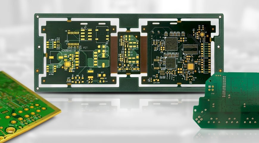
Electronics are getting smaller, lighter, and more complex. With this evolution, traditional rigid circuit boards are sometimes not the best solution. Flexible circuits offer a more durable, space-saving alternative that can withstand bending, twisting, and harsh environments.

For engineers and manufacturers, electronic PCB design must focus on durability and reliability. Whether used in wearables, medical devices, automotive electronics, or industrial applications, flexible circuits provide a significant advantage. PCB circuit board manufacturers are now integrating flexible PCBs into designs to enhance performance and longevity.

This blog will discuss how flexible circuits improve durability in electronics and why they are becoming a go-to solution in electronic PCB manufacturing.

What Are Flexible Circuits?

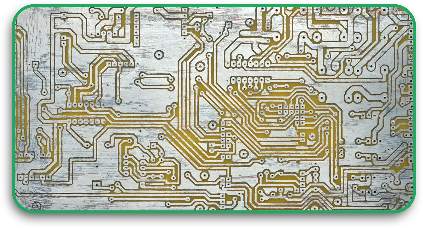
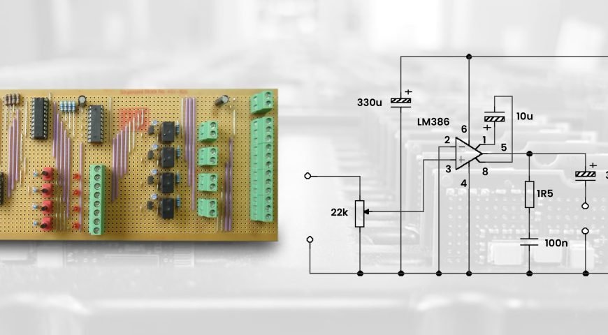
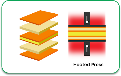
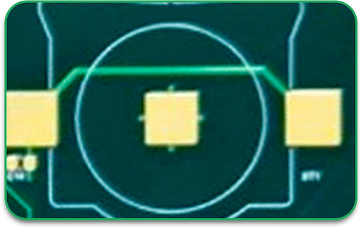
A flexible circuit, also called a flex PCB, is a type of printed circuit board that can bend, twist, and fold without breaking. Unlike traditional rigid multilayer PCBs, these circuits use thin, flexible materials such as polyimide or PET film instead of FR-4. These circuits allow for better space utilisation, improved shock resistance, and increased mechanical durability. They are widely used in electronic PCB circuits for applications where flexibility, weight reduction, and reliability are essential.

flex pcb stackup

Why Durability Matters in Electronics

1. Reducing Mechanical Stress

In rigid circuit boards, repeated vibrations or impacts can cause solder joints to crack, leading to device failure. Flexible circuits, however, are designed to absorb stress, making them perfect for electronic assembly PCBs used in automotive and aerospace applications.

2. Resistance to Environmental Factors

Flexible PCBs are often coated with protective layers that make them resistant to moisture, dust, and extreme temperatures. This feature is critical for electronic PCB manufacturing in industries like medical electronics and outdoor sensor devices.

3. Extended Lifespan

Because flexible circuits eliminate the need for bulky connectors and reduce the number of solder joints, they have fewer failure points, leading to longer-lasting electronic devices.

How Flexible Circuits Improve Durability in Electronics

1. Withstand Repeated Bending and Flexing

Unlike traditional multilayer PCBs, which can crack under repeated stress, flexible circuits can handle thousands of bending cycles without damage. This durability makes them ideal for wearable technology, foldable devices, and medical implants.

2. Enhanced Shock and Vibration Resistance

Electronics used in automotive, aerospace, and military applications experience high levels of vibration. Flexible circuits are designed to withstand these conditions, making them ideal for mission-critical systems.

3. High-Temperature Resistance

Polyimide-based flexible circuits have excellent heat resistance, which makes them suitable for harsh industrial environments where temperature fluctuations can cause traditional PCBs to fail.

4. Reduced Weight and Thickness

Because flexible circuits are thinner and lighter than traditional PCBs, they allow for compact electronic PCB design, making them perfect for portable medical devices, drones, and smartphones.

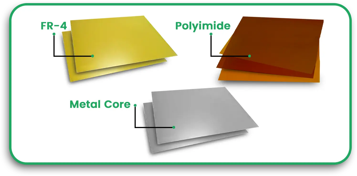
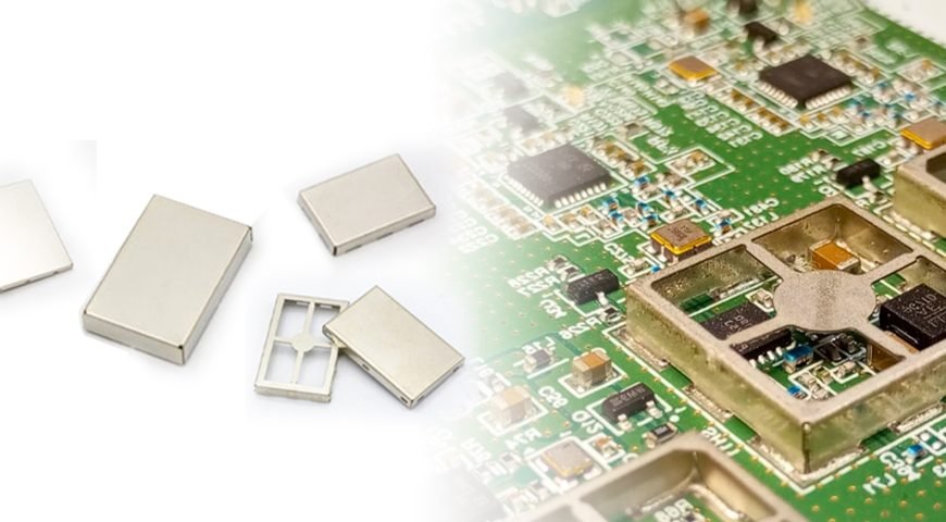
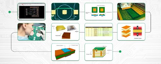
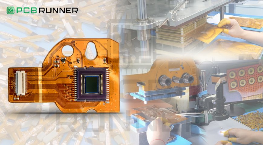
Materials Used in Flexible Circuit Fabrication

To achieve durability and flexibility, PCB circuit board manufacturers use specialised materials in electronic PCB manufacturing.

1. Substrates

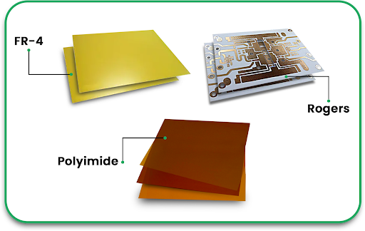
  • Polyimide (PI): The most common material used for flexible circuits, offering high heat resistance and durability.
  • Polyethylene Terephthalate (PET): Used in lower-cost applications, offering moderate flexibility but lower heat resistance.

2. Conductive Layers

  • Copper Foil: Standard choice for conducting layers in flexible circuits.
  • Silver Ink: Used in low-cost, low-power applications.

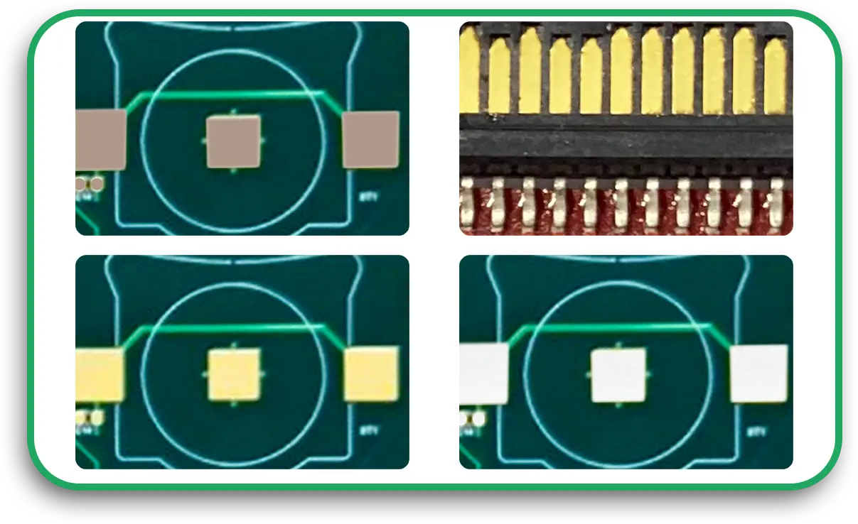
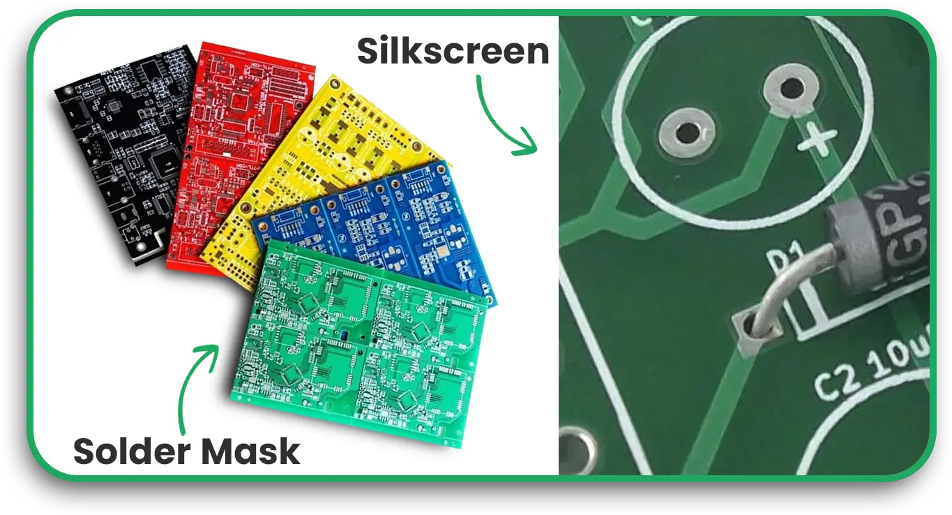
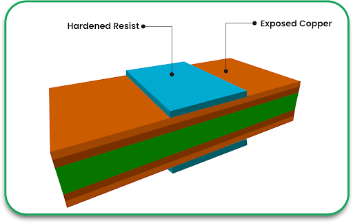
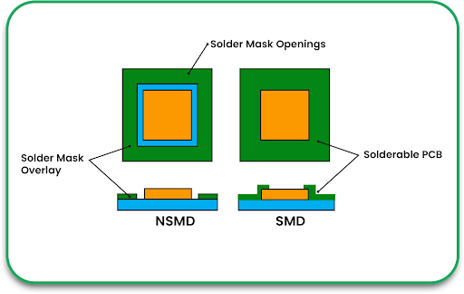
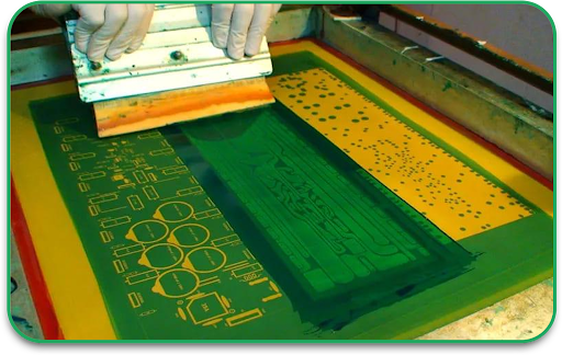
3. Protective Layers

  • Solder Mask Material: Prevents oxidation and short circuits.
  • Conformal Coating: Adds a protective barrier against moisture and dust.

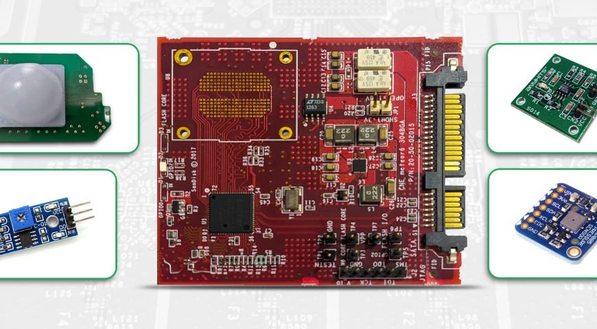
Key Applications of Flexible Circuits in Electronics

1. Wearable Electronics

From fitness trackers to smart glasses, flexible circuits make it possible to design compact, lightweight devices that can be worn comfortably while withstanding everyday wear and tear.

2. Medical Devices

Many medical implants and diagnostic devices require highly durable and biocompatible electronic circuits. Flexible PCBs help ensure these devices function reliably over long periods.

3. Automotive Electronics

Modern vehicles rely on electronic assembly PCBs for navigation systems, sensors, and advanced driver-assistance systems (ADAS). Flexible circuits improve reliability in high-vibration environments.

4. Aerospace and Military Applications

Satellites, aircraft, and defence equipment require multilayer PCBs that can survive extreme conditions. Flexible circuits provide durability and weight savings in these applications.

5. Consumer Electronics

Smartphones, laptops, and cameras use flexible circuits for improved space efficiency and device longevity.

How to Optimise Flexible Circuit Design for Durability

1. Choose the Right Material

Selecting high-quality polyimide or PET substrates ensures better flexibility and temperature resistance.

2. Use Reinforced Traces

Adding copper plating or protective coatings helps prevent cracks and improves durability.

3. Optimise Bending Areas

Design circuits with curved, gradual bends rather than sharp angles to prevent stress fractures.

4. Minimise Connectors and Solder Joints

Reducing the number of connectors eliminates potential failure points, making electronic PCB circuits more reliable.

5. Implement Stress-Relief Features

Adding strain relief structures in key areas prevents excessive mechanical stress on the circuit. For example, using anchor pads at solder joints can help distribute mechanical load more evenly.

6. Use Protective Coatings

Applying solder mask material or conformal coatings can protect the electronic PCB circuit from environmental damage, such as moisture, dust, and chemicals.

7. Optimise Trace Width and Spacing

Ensuring the proper trace width and spacing prevents overheating and signal interference, which is especially important in high-density multilayer PCB designs.

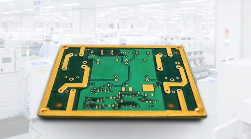
Flexible Circuit vs. Traditional Rigid PCB: A Durability Comparison

Feature Flexible Circuit Rigid PCB
Bendability Highly flexible, can bend repeatedly Cannot bend, will break under stress
Shock Resistance Absorbs vibrations and impact Susceptible to cracks and fractures
Weight & Thickness Lighter and thinner Bulkier and heavier
Temperature Resistance Withstands high and low temperatures Can degrade in extreme conditions
Durability in Harsh Environments High Moderate

While rigid PCBs are ideal for applications requiring structural strength, flexible circuits offer superior durability and versatility in demanding environments.

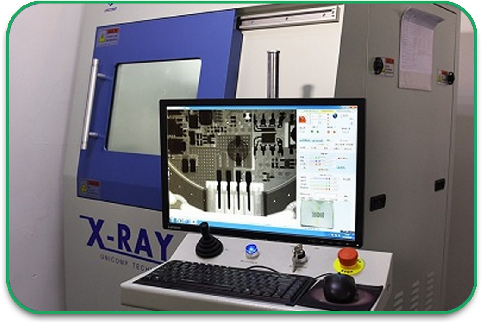
Manufacturing Challenges and Solutions for Flexible Circuits

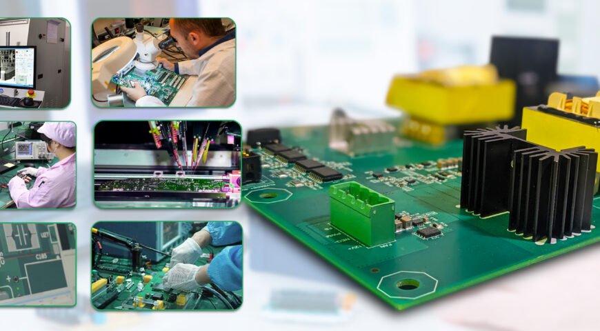
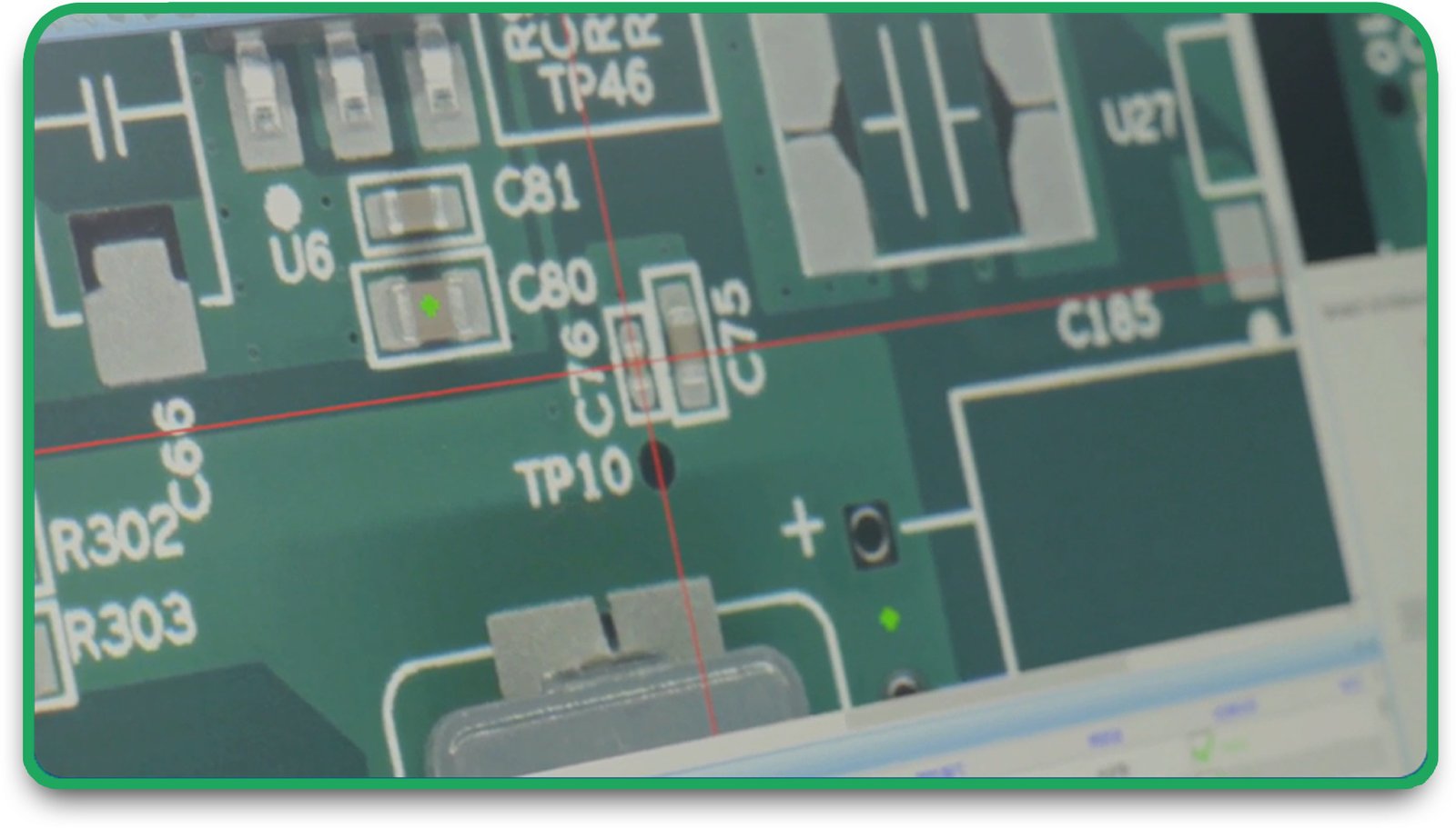
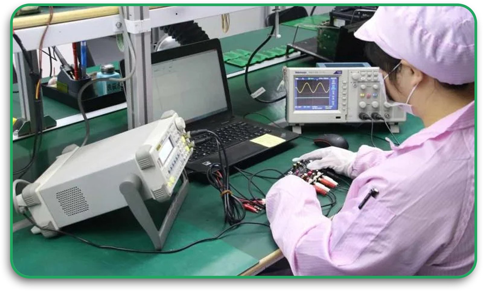
Although flexible circuits provide many benefits, their manufacturing process comes with certain challenges. Here’s how PCB circuit board manufacturers address them:

1. Handling Thin Substrates

Flexible PCBs use ultra-thin substrates that can wrinkle or tear. Solution: Using supporting carriers during fabrication prevents damage.

2. Achieving Consistent Plating

Because flexible circuits bend, ensuring even copper plating can be difficult. Solution: Advanced plating techniques and controlled chemical baths improve consistency.

3. Preventing Signal Interference

High-speed electronic PCB circuits require proper shielding to avoid electromagnetic interference (EMI). Solution: Using ground planes and shielding layers improves signal integrity.

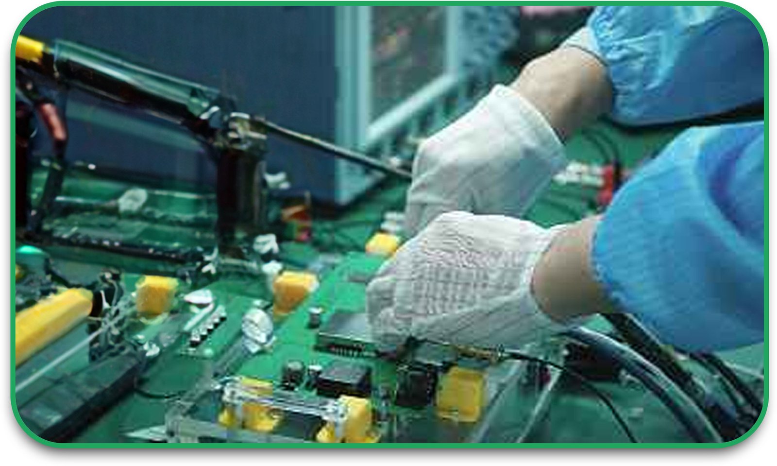
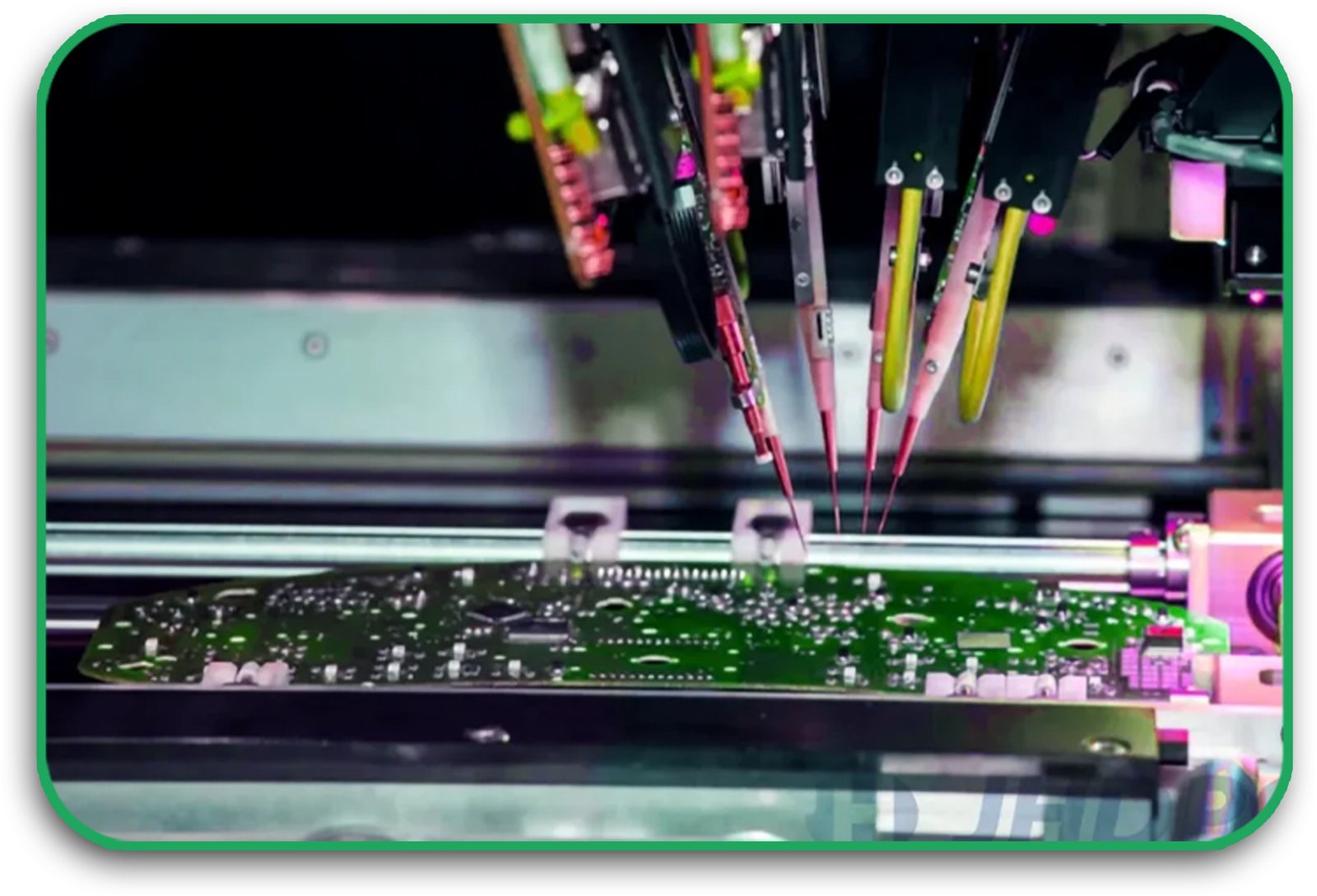
4. Optimising Assembly Process

Flexible PCBs require careful handling during circuit board assembly to avoid misalignment or damage. Solution: Automated precision equipment ensures accurate component placement.

Future Trends in Flexible PCB Technology

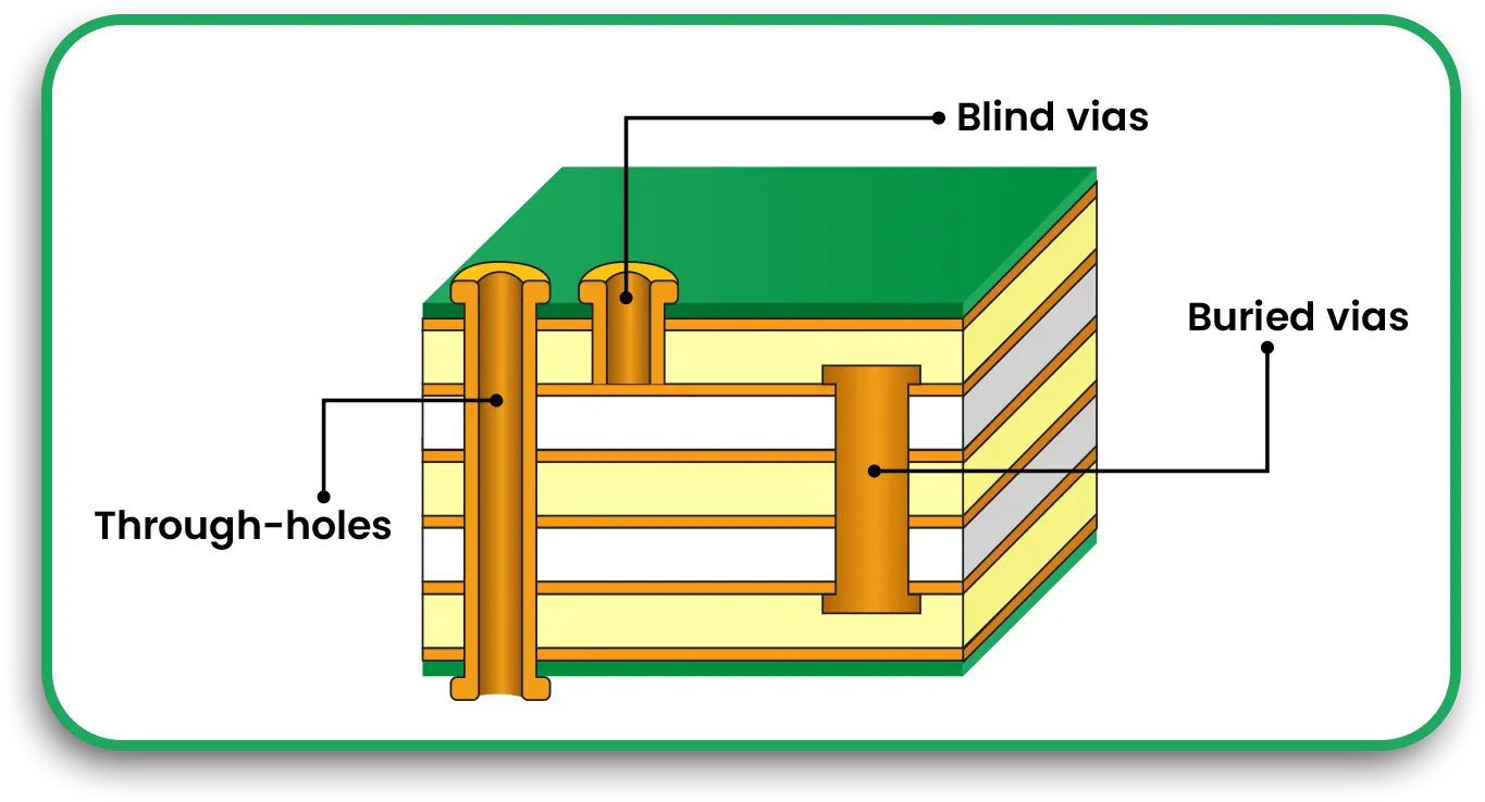
1. Increasing Use of High-Density Interconnect (HDI) PCBs

As electronics continue to shrink, HDI multilayer PCBs with microvias and ultra-fine traces will be essential for next-generation devices.

2. Printed Electronics and Conductive Inks

Innovations in conductive ink technology are enabling flexible hybrid electronics, where printed circuits replace traditional copper traces.

3. Stretchable Electronics

Next-gen stretchable PCBs will revolutionise wearables and medical implants, offering even greater durability and adaptability.

4. Enhanced Materials for Extreme Environments

Future flexible circuits will use advanced polymers and nanomaterials to withstand higher temperatures and radiation exposure in aerospace and industrial applications.

Conclusion

Flexible circuits are transforming the electronics industry by offering unmatched durability, lightweight designs, and improved reliability. Whether for wearable technology, medical devices, or aerospace systems, these circuits provide a long-lasting and space-saving solution. As electronic PCB manufacturing continues to evolve, flexible PCBs will play an even bigger role in high-performance applications. If you need custom printed circuit boards that prioritise durability and efficiency, flexible circuits are the way to go.

Looking for Reliable Flexible PCB Solutions?

At PCB Runners, we specialise in high-quality PCB fabrication for flexible circuits, multilayer PCBs, and custom designs. Contact us today to get started on your next circuit board assembly project.

Frequently Asked Questions (FAQs)

1. What makes flexible PCBs more durable than rigid PCBs?
Flexible PCBs can bend and absorb stress, making them more resistant to mechanical damage and environmental factors like heat and moisture.

2. Can flexible circuits replace traditional rigid PCBs?
In some applications, yes. Flexible circuits are ideal for wearables, medical devices, and aerospace, but rigid PCBs are still necessary for high-structural integrity applications.

3. What are the common materials used in flexible PCB manufacturing?
Flexible PCBs use polyimide (PI), PET film, and conductive copper layers to ensure durability and flexibility.

4. How can I ensure my flexible PCB lasts longer?
Use high-quality materials, apply protective coatings, minimise stress points, and follow best practices in electronic PCB design.

5. Are flexible circuits more expensive than rigid PCBs?
Initially, flexible circuits may cost more due to specialised materials and processes, but they reduce overall costs by eliminating connectors and improving reliability.

PCB Fabrication and Assembly

High-Quality PCB Fabrication and Assembly

The demand for high-quality PCB fabrication and assembly is growing rapidly as modern electronics become more complex and compact. Whether you’re designing consumer gadgets, medical devices, or industrial equipment, the circuit board assembly process plays a crucial role in ensuring the reliability and performance of your product.

Choosing the right PCB assembly manufacturer and using the best PCB assembly services can make a significant difference in product quality, durability, and efficiency. In this guide, we will explore the PCB fabrication process, assembly techniques, and key considerations to achieve high-quality PCB printed circuit board assembly.

What is PCB Fabrication?

PCB fabrication is the process of manufacturing printed circuit boards from raw materials like copper, fiberglass, and solder mask. This process involves multiple steps, including designing the board, etching copper traces, drilling holes, and applying protective coatings.

A well-fabricated PCB ensures optimal electrical performance, mechanical strength, and thermal management. The fabrication process must be precise, as even a small error can impact the entire circuit’s functionality.

Key Steps in PCB Fabrication

1. PCB Design and Layout

Before fabrication begins, engineers use PCB design software to create the board layout. This includes defining trace widths, hole placements, and layer stack-ups.

PCB Design and Layout stackup

2. Preparing the Substrate

The board’s core material, typically FR-4 (fiberglass-reinforced epoxy), polyimide, or metal, is selected based on application requirements.

Preparing the Substrate

3. Copper Cladding and Etching

A thin copper layer is laminated onto the board, and unwanted copper is etched away to form conductive pathways.

Copper Cladding and Etching

4. Drilling Holes

Holes are drilled for mounting components and vias, which connect different layers in multilayer PCBs.

Plating and Surface Finishing

5. Plating and Surface Finishing

Copper-plated vias and surface finishes, such as ENIG (Electroless Nickel Immersion Gold) or HASL (Hot Air Solder Leveling), improve conductivity and durability.

Drilling Holes

6. Solder Mask and Silkscreen Application

The solder mask protects copper traces, while the silkscreen layer adds component labels and reference marks.

Solder Mask and Silkscreen Application

7. Final Inspection and Testing

Each PCB undergoes electrical and optical testing to ensure it meets design specifications before moving to circuit board assembly.

Final Inspection and Testing

What is PCB Assembly?

PCB assembly (PCBA) is the process of mounting and soldering electronic components onto a fabricated circuit board. This step is critical in turning a bare PCB into a fully functional electronic circuit.

A reliable PCB assembly manufacturer follows strict quality control procedures to prevent soldering defects, misaligned components, or poor electrical connections.

Key PCB Assembly Methods

1. Surface Mount Technology (SMT)

  • Uses automated machines to place small components onto the board’s surface.
  • Ideal for compact, high-density designs.
  • Faster and more cost-effective than traditional through-hole assembly.

2. Through-Hole Technology (THT)

  • Components with leads are inserted into pre-drilled holes and soldered in place.
  • Provides stronger mechanical bonds, making it ideal for high-stress environments.

3. Mixed Technology Assembly

  • Combines SMT and THT for optimal performance and reliability.
  • Used in aerospace, medical, and industrial applications requiring both miniaturisation and durability.

Essential Factors for High-Quality PCB Assembly

1. Choosing the Right PCB Assembly Manufacturer

A trusted PCB assembly manufacturer ensures precision, reliability, and compliance with industry standards. Look for certifications such as ISO 9001, IPC-A-610, and RoHS compliance.

2. Component Sourcing and Quality Control

Using high-quality, genuine components prevents failures and ensures long-term reliability.

3. Optimised PCB Design for Assembly (DFA)

Designing for efficient assembly reduces defects and improves yield. Consider factors such as proper pad sizing, component spacing, and thermal relief.

4. Effective Soldering Techniques

Reliable PCB assembly services use reflow soldering for SMT components and wave soldering for through-hole components to create strong electrical connections.

5. Testing and Inspection

  • Automated Optical Inspection (AOI) detects misalignments and solder defects.
  • X-ray Inspection checks hidden solder joints in BGA and high-density PCBs.
  • Functional Testing ensures the assembled PCB performs as expected.

Benefits of High-Quality PCB Assembly

1. Enhanced Reliability

Proper PCB fabrication and assembly techniques prevent short circuits, solder cracks, and component failures, ensuring long-term durability.

2. Improved Electrical Performance

Precision assembly ensures optimal signal integrity, reducing noise and interference in high-speed applications.

3. Faster Time-to-Market

Efficient PCB assembly services streamline production and reduce design revisions, accelerating product development.

4. Cost Savings

Minimising assembly defects reduces rework and production waste, leading to lower manufacturing costs.

5. Scalability for Mass Production

Reliable PCB assembly manufacturers can handle high-volume orders while maintaining consistency and quality.

Latest Innovations in PCB Fabrication and Assembly

1. High-Density Interconnect (HDI) PCBs

HDI PCBs feature smaller traces, microvias, and stacked layers, allowing for compact and high-performance circuit designs.

2. Flexible and Rigid-Flex PCBs

Flexible PCBs improve durability in wearable devices, aerospace, and automotive applications.

3. Lead-Free Soldering

With growing environmental concerns, manufacturers are shifting to RoHS-compliant, lead-free soldering techniques.

4. AI-Driven Quality Control

Artificial intelligence (AI) is improving defect detection and process optimisation in modern PCB assembly lines.

5. Automated Assembly for Faster Production

Fully automated circuit board assembly increases efficiency and reduces human errors, improving overall yield.

Conclusion

High-quality PCB fabrication and assembly is essential for developing reliable, high-performance electronics. From advanced PCB fabrication techniques to precise assembly methods, every step plays a vital role in ensuring product success.By partnering with a trusted PCB assembly manufacturer, you can achieve faster production, improved quality, and cost-effective solutions for your electronic projects.

Looking for Expert PCB Fabrication and Assembly?

At PCB Runners, we specialise in custom PCB fabrication, circuit board assembly, and high-reliability PCB solutions. Contact us today to discuss your PCB assembly needs and get a free quote.

Frequently Asked Questions (FAQs)

1. What is the difference between PCB fabrication and PCB assembly?
PCB fabrication is the process of manufacturing the bare board, while PCB assembly involves mounting electronic components onto the fabricated board.

2. What factors affect PCB assembly quality?
Key factors include design optimisation, component quality, precise soldering, and thorough testing procedures.

3. How do I choose the best PCB assembly manufacturer?
Look for certifications, industry experience, component sourcing capabilities, and quality control measures when selecting a PCB assembly manufacturer.

4. What are the advantages of multilayer PCBs in assembly?
Multilayer PCBs offer higher circuit density, improved signal integrity, and better heat dissipation, making them ideal for advanced electronic applications.

5. Why is functional testing important in PCB assembly?
Functional testing ensures the assembled PCB works as intended, preventing failures in real-world applications.

Wearable Electronics

Essential PCB Assembly Techniques for High-Performance Wearable Electronics

Wearable technology is transforming the way we interact with electronics, from smartwatches and fitness trackers to medical monitoring devices and augmented reality glasses. These devices require Multilayer PCBs that are lightweight, compact, and durable while maintaining excellent electrical performance. The assembly of a Custom Printed Circuit Board for wearables involves specialized techniques to ensure flexibility, reliability, and power efficiency. 

As demand for wearable PCB solutions continues to grow, engineers and manufacturers must adopt the best Circuit Board Assembly practices to create high-performance wearable electronic devices. This guide covers essential electronic PCB assembly techniques to improve functionality, durability, and overall performance. 

Key Requirements for Wearable PCBs 

1. Compact and Lightweight Design

Wearable devices have strict size and weight limitations. PCBs must be thin, flexible, and designed for minimal power consumption. Multilayer PCBs are commonly used to maximize functionality while maintaining a compact footprint. 

2. Flexibility and Durability

Since wearables experience constant movement, wearable PCBs must withstand bending and flexing without losing functionality. Flexible PCBs or Rigid-Flex PCBs offer improved durability by combining rigid and flexible layers into a single board. 

3. Efficient Power Management

Wearable devices operate on small batteries, requiring PCBs with low power consumption. Efficient Circuit Board Assembly ensures minimal energy loss and optimized battery life. 

4. Reliable Electronic Component Placement

Properly placing and soldering electronic components PCB is critical for the durability of wearable electronics. Using advanced electronic PCB assembly methods like Surface Mount Technology (SMT) improves accuracy and reliability. 

PCB Assembly Techniques for Wearable Electronics 

1. Using Flexible PCBs

Unlike traditional rigid PCBs, wearable PCB designs often incorporate flexible PCBs to accommodate movement. These boards allow wearable devices to fit comfortably on the body without breaking or losing electrical connectivity. 

Advantages of Flexible PCBs: 

  • Lightweight and space-saving
  • Resistant to bending and flexing
  • Ideal for compact wearable electronic devices 

2. Rigid-Flex PCB Technology

For applications requiring both durability and flexibility, Rigid-Flex PCBs combine stiff and flexible sections into a single Multilayer PCB. These hybrid boards reduce the need for additional connectors and cables, improving reliability. 

Benefits of Rigid-Flex PCBs: 

  • Enhanced structural integrity
  • Reduced component failures
  • Ideal for fitness trackers and medical wearables 

3. Surface Mount Technology (SMT) Assembly

SMT is the preferred method for electronic PCB assembly in wearable electronics. It allows for the placement of miniaturized components directly onto the PCB surface, reducing weight and improving electrical performance. 

Why SMT is Ideal for Wearable PCBs: 

  • Supports high-density component placement
  • Improves electrical performance and signal integrity
  • Reduces the overall weight of the PCB 

4. Low-Power Design Techniques

Since wearables rely on battery power, Custom Printed Circuit Board designs must incorporate low-power consumption techniques. 

Power Optimization Methods: 

  • Use energy-efficient microcontrollers and sensors
  • Optimize power distribution with embedded passive components \
  • Implement low-power communication protocols like Bluetooth Low Energy (BLE) 

5. Miniaturized Component Placement

As wearable devices become smaller, PCBs must accommodate electronic components PCB with ultra-fine pitches. High-precision Circuit Board Assembly techniques such as Microvia Technology and High-Density Interconnect (HDI) PCBs enable better performance in compact designs. 

Advantages of Miniaturized Components: 

  • Maximizes space efficiency
  • Improves signal transmission speed
  • Enhances device aesthetics with slimmer designs
  • Material Considerations for Wearable PCB Assembly 

Selecting the right materials is crucial for manufacturing durable wearable electronic devices: 

1. Substrate Materials

Wearable PCBs often use polyimide or liquid crystal polymer (LCP) instead of traditional FR-4. These materials provide flexibility, heat resistance, and improved electrical performance. 

Common Substrate Choices: 

  • Polyimide: High flexibility and heat resistance
  • LCP: Low moisture absorption and excellent signal integrity
  • FR-4: Suitable for rigid sections of hybrid PCBs 

2. Conductive Materials

To ensure optimal electrical performance, wearable PCBs use copper foils with different thickness levels based on current requirements. 

Common Conductive Layers: 

  • Standard copper foils for low-power applications 
  • Heavy copper PCB layers for power-intensive sections 

3. Protective Coatings

Wearable PCBs require protective coatings to safeguard components from sweat, moisture, and physical impact. 

Types of Protective Coatings: 

  • Conformal Coatings: Protect against dust, moisture, and mechanical stress 
  • Encapsulation (Potting): Provides additional insulation and protection 
  • Solder Mask Material: Prevents solder bridging and oxidation 

Challenges in Wearable PCB Assembly 

1. Heat Dissipation in Compact Designs

Wearable devices have limited space for heat sinks. PCB manufacturers use thermal vias and graphene-based heat spreaders to dissipate heat efficiently. 

2. Component Durability

Since wearables are constantly exposed to motion, electronic components PCB must withstand vibrations and impacts. Using reinforced Circuit Board Assembly techniques helps improve resilience. 

3. Signal Integrity and Interference

High-speed data transmission in wearables requires careful PCB layout design. Shielding techniques and High-Density Interconnect (HDI) PCBs help minimize signal loss and electromagnetic interference (EMI). 

Future Trends in Wearable PCB Assembly 

1. Stretchable and Biocompatible PCBs

New materials such as stretchable polymers and biocompatible substrates are expanding the possibilities of wearable electronics, particularly in medical applications. 

2. Printed Electronics and Flexible Hybrid Electronics (FHE)

Innovations in printed circuit technologies enable cost-effective, lightweight, and customizable wearable PCBs for next-generation smart devices. 

3. AI-Driven PCB Assembly Automation

AI-powered electronic PCB assembly is enhancing manufacturing precision, reducing defects, and improving yield rates in high-performance wearable electronics. 

Conclusion 

High-performance wearable PCB design requires a combination of advanced materials, compact layouts, and precise electronic PCB assembly techniques. By leveraging Multilayer PCBs, Rigid-Flex PCBs, and low-power design methods, manufacturers can create reliable wearable electronic devices that perform well in real-world conditions. For engineers and designers looking to optimize Circuit Board Assembly for wearables, working with experienced PCB manufacturers ensures high-quality fabrication, enhanced durability, and seamless integration of miniaturized components. 

Need High-Quality Wearable PCBs? 

PCB Runners specializes in Custom Printed Circuit Board solutions for wearable technology. Whether you need Multilayer PCBs, Flex and Rigid PCBs, or specialized Circuit Board Assembly, our expert team is ready to help. Contact us today to discuss your project needs. 

Frequently Asked Questions (FAQs) 

1. What type of PCB is best for wearable electronics?
Flexible PCBs and Rigid-Flex PCBs are ideal for wearable devices because they allow movement without breaking.

2. Why is low power consumption important in wearable PCBs?
Wearables run on small batteries, so low-power PCB designs extend battery life and improve efficiency.

3. How do you protect wearable PCBs from moisture?
Protective coatings like conformal coatings and encapsulation shield PCBs from sweat and environmental exposure.

4. What is the best soldering method for small wearable PCBs?
Surface Mount Technology (SMT) is preferred for its high precision and ability to handle miniaturized components.

5. Where can I get a custom wearable PCB manufactured?
PCB Runners offers professional wearable PCB manufacturing and assembly services with fast turnaround times. Contact us for a quote today.

Veroboard Circuit Design

Veroboard Circuit Design: Advantages and Key Considerations for PCB Projects

When working on electronic projects, you need a reliable way to build and test circuits before full production. While multilayer printed circuit boards are used for complex electronics, many engineers and hobbyists prefer Veroboard PCBs for prototyping. Veroboard, also known as stripboard, provides a simple and cost-effective solution for designing circuits without the need for professional PCB circuit board manufacturers.

Unlike flex and rigid PCB solutions, Veroboard does not require advanced fabrication. Instead, it allows you to manually build circuits by placing and soldering components onto a pre-drilled board with copper tracks. If you are new to Veroboard circuit design, understanding how it works can help you determine if it is the right choice for your project.

This guide explains how Veroboard works, its advantages, limitations, and key considerations to keep in mind when designing your circuit.

What is Veroboard?

Veroboard is a type of perforated circuit board with copper strips running along one side. These strips act as electrical connections between components. Unlike a custom printed circuit board, Veroboard does not require professional printed circuit board design software or specialized fabrication processes.

Main Features of Veroboard:

  • Pre-drilled holes for easy component placement 
  • Copper tracks for electrical connections 
  • Requires manual cutting and soldering 
  • Supports through-hole components 

This makes Veroboard an excellent choice for simple circuits and testing before committing to full circuit board assembly

Advantages of Veroboard Circuit Design

1. Easy to Use and Modify

Veroboard is much simpler to use than designing a multilayer printed circuit board. You can quickly make changes, add new components, or rework your design without professional manufacturing tools.

2. Cost-Effective Prototyping

Building a custom printed circuit board can be expensive, especially for small projects. Veroboard allows you to prototype ideas without high costs. 

3. No Special Software Required

Unlike printed circuit board design software, Veroboard lets you design directly on the board. You don’t need complex software tools or expensive licenses. 

4. Ideal for Small Projects

If you are building a simple circuit, Veroboard is often a more practical option than a fully fabricated flex and rigid PCB. 

Key Considerations for Veroboard Circuit Design

While Veroboard is useful, it also has limitations. Knowing these can help you design reliable circuits with fewer mistakes. 

1. Careful Layout Planning

Unlike a multilayer printed circuit board, Veroboard lacks complex routing options. Planning component placement is essential to avoid overlapping connections. 

2. Cutting Tracks Correctly

Since Veroboard has continuous copper strips, you must cut them at specific points to create separate electrical paths. Use a track cutter or sharp blade for precise cuts. 

3. Space Between Components

Unlike professional circuit board assembly, Veroboard requires manual soldering. Keep components spaced properly to avoid shorts and overheating. 

4. Limited to Through-Hole Components

Veroboard is not designed for surface-mount components. If your project requires a high-density interconnect layout, a professionally made custom printed circuit board is a better choice. 

5. No Dedicated Ground or Power Planes

A multilayer printed circuit board includes layers for power and ground connections, improving signal integrity. Veroboard lacks this, making it more prone to interference. 

How to Design a Veroboard Circuit

Step 1: Plan Your Circuit

Sketch your circuit on paper or use a simple digital tool to plan where each component will go. Ensure that tracks do not cross unnecessarily. 

Step 2: Arrange Components on the Board

Place components strategically to reduce wiring complexity. Keep related parts close together. 

Step 3: Cut Copper Tracks

Use a track cutter or sharp knife to break unnecessary connections. Double-check before soldering. 

Step 4: Solder Components

Secure each component with solder, ensuring clean and reliable joints. Avoid excess solder that could cause short circuits. 

Step 5: Test the Circuit

Before applying power, use a multimeter to check for shorts or incorrect connections. Fix any errors before turning on the circuit. 

Veroboard vs. Custom PCB Manufacturing

Feature  Veroboard  Custom PCB (Fabricated by PCB Circuit Board Manufacturers) 
Ease of Use  Simple, requires manual soldering  Requires PCB design software and professional fabrication 
Cost  Low  Higher, but more scalable for production 
Component Type  Through-hole only  Supports through-hole and surface-mount 
Customization  Limited  Fully customizable layouts 
Durability  Moderate  High 
Signal Integrity  Lower  Higher 

Veroboard is best for quick prototyping, while a professionally fabricated PCB is better for long-term projects and mass production. 

When to Use Veroboard vs. PCB Fabrication 

Use Veroboard When:

  • You need a fast and low-cost prototype 
  • The circuit is simple and does not require advanced routing 
  • You are experimenting or learning about electronics 

Use a Custom PCB When:

  • You need compact layouts with surface-mount components 
  • The project requires reliable, mass-produced boards 
  • High signal integrity and performance are critical 

Common Mistakes to Avoid with Veroboard

  • Skipping Layout Planning: Leads to messy wiring and errors 
  • Not Cutting Tracks Properly: Can create electrical shorts 
  • Overheating Components While Soldering: Damages sensitive parts 
  • Ignoring Testing Before Powering On: Always check connections first 

Avoiding these mistakes will help ensure your Veroboard circuit design is functional and easy to troubleshoot. 

Conclusion 

Veroboard is an excellent choice for quick and affordable prototyping. It allows you to test ideas before committing to a fully fabricated multilayer printed circuit board. While it has limitations, proper planning and careful assembly can make Veroboard a powerful tool for hobbyists and engineers alike.

If you need a custom printed circuit board for high-performance applications, working with PCB circuit board manufacturers is the best choice. They can provide optimized designs with better durability and performance. 

Looking for a Custom PCB? 

PCB Runners offers high-quality PCB fabrication services for all applications. Whether you need a multilayer printed circuit board or a flex and rigid PCB, we can help. Contact us today for expert support. 

Frequently Asked Questions (FAQs)

1. What is the difference between Veroboard and a custom PCB?
Veroboard is a perforated board with copper strips, while a custom printed circuit board is professionally designed and manufactured for specific layouts.

2. Can Veroboard be used for high-frequency circuits?
No, Veroboard lacks dedicated ground planes and shielding, making it unsuitable for high-frequency applications.

3. How do I cut tracks on Veroboard?
Use a track cutter or a sharp knife to break copper connections where necessary.

4. Can I use surface-mount components on Veroboard?
Veroboard is designed for through-hole components. Surface-mount parts require adapters or alternative mounting methods.

5. Where can I get a custom PCB made?
PCB Runners specializes in custom PCB fabrication for all applications. Contact us for a quote today.

Design a Macropad PCB

How to Design a Macropad PCB: A Step-by-Step Guide

A macropad PCB is a miniaturized circuit board intended for personalized input devices that let users set macros, shortcuts, or hotkeys for a more efficient workflow. Custom slabs of a macropad PCB can significantly increase efficiency in gaming, video editing, and coding.  The creation of a macropad PCB design necessitates appropriate printed circuit board design software, selection of solder mask material, and reputable PCB manufacturers for fabrication. Given the competition for high-density interconnect (HDI) technology, modern methods of assembling circuit boards result in easily fabricated and reliable macropods. 

This blog will cover everything from designing the layout to doing the final assembly. 

Step 1: Basics of a Macropad PCB 

A macropad PCB acts as a small keyboard that has programmable keystrokes or buttons. A macropad can be compared to a keyboard, and it too has keys, albeit lesser in number, approximately 3-20, that are designed for certain operations. 

Main Parts Of A Macropad PCB 

  • Microcontroller Unit (MCU) :The controller of a macropad that reads the key press. 
  • Switches: Mechanical or capacitive switches that detect the input. 
  • Diodes: Employed in the switch matrix for ghosting protection. 
  • Traces and Vias: Pathways that connect components electrically. 
  • USB Connector: The means through which the macropad interfaces with the computer. 
  • LEDs (Optional): Provides backlight or indicator function for a user interface. 

Through learning these components, one is set to design an efficient and functional macropad PCB. 

Step 2: Selection of Printed Circuit Board Design Software 

  • For macropad PCB design, you would need specialized printed circuit board design software with both schematic capture and edit layout functions. Some you may consider are: 
  • KiCad : It is free and open source that is widely used on custom PCBs 
  • Eagle: This is more sophisticated software with a rich components library. 
  • Altium Designer:  It is top-of-the-range professional printed circuit board design software. 
  • EasyEDA: This is good for first-time users, and it is web-based. 

Select the one that corresponds to your level of experience and approach to the project. 

Step 3: Forming the Macropad Schematic 

A schematic is a diagram which shows how components are linked together. This is how you draw it in your printed circuit board design software: 

Place the Microcontroller: Popular candidates are ATmega32U4 or RP2040, which both can accept USB input. 

  • Add Switches: Decide and set the number of keys and how they will be aligned. 
  • Include Diodes: These avoid interference that can happen from a switch matrix. 
  • Draw Power and Ground Connections: These are essential to ensure good power distribution. 
  • Define the USB Interface: Choose a USB-C or Micro-USB socket. 

After the schematic is done, conduct electrical checks before you proceed to the PCB layout. 

Step 4: Designing the PCB Layout 

1. Establish Board Sizes

You have to scale and contour your macropad PCB in relation to your case and key arrangement so you figure out its size. 

2. Place the Components

  • Traces should be as short and straight as possible to reduce signal degradation.
  • Place diodes near switches to tidy up the layout.
  • Adjust components for efficient soldering and assembly. 

3. Route Traces and Vias

  • Use interconnection techniques for compact designs – High-density interconnects (HDI).
  • Trace gaps must be sufficient to avoid shorting between them.
  • Deploy ground planes for lower noise and improved stability. 

4. Choose Appropriate Solder Mask Material

The solder mask material is in charge of preventing the PCB from oxidizing and covering solder bridge accidents. Usual choices are: 

Epoxy Liquid: It is cheap, but it can be brittle. 

Liquid Photoimageable (LPI) Solder Mask – Capable of great precision. 

Dry Film Solder Mask: Best for high-density interconnect PCBs. 

Select a solder mask material that best meets production requirements. 

Step 5: Getting Ready for PCB Manufacturing 

These are the two additional tasks that need to be performed before sending the board to the PCB manufacturer: 

  • Execute a Design Rule Check (DRC) – Validate that there are no design infringements.
  • Examine the Trace Width and Trace Spacing – How their values comply with the acceptable fabrication ones.
  • Create Gerber Files – a must for PCB design fabrication. 

Once you have completed verifying the design, send it to a reliable PCB board manufacturer for construction. 

Step 6: Circuit Board Assembly 

With the macropad PCB fabricated, you are now ready to assemble the circuit board (CBA). You can choose to: 

  • Solder Components by Hand – Ideal for hobbyists or small-volume production.
  • Outsource to a PCB Assembly Contractor – Best for larger quantities. 

Key Steps in Circuit Board Assembly: 

  • Solder Paste Application – For use with surface mount components.
  • Component Placement – Brought in with the aid of pick-and-place robots or done manually with tweezers. 

Soldering Reflow: Heats solder to install components. 

  • Soldering Through-Hole – Applicable to diodes and switches.
  • Final Checks and Verification – Validates functionality of all the solder joints. 

Step 7: Programming the Macropad 

After the PCB is transferred, it needs some firmware to operate. Some of the more common choices are: 

  • QMK – Customizable for various uses.
  • VIA Firmware – User-friendly software interface to configure keys.
  • Arduino IDE – Friendly for use with simpler tasks. 

Procedure to Flash the Firmware: 

  • Plug in the Macropad via USB to a computer.
  • Get the needed Drivers Support for the microcontroller.
  • Inject Firmware with QMK Toolbox or similar software. 

Verify Functionality by pressing all the keys to check whether they work. 

STEP 8: Final Examination and Problem Fixing 

Running a test on a macropad PCB requires several steps. The first step is testing: 

Basic Tests: 

  • Continuity TestChecks if the traces have continuity. 
  • Keypress Test – Checks if the switches output as expected.
  • USB Connection Test – Tests a device’s ability to communicate with the host computer.  
Helpful Hints: 

Registering issues? You may want to look for solder joints and diodes.  

No USB connection? Check your firmware configuration and trace the wires.  

If everything else is fine but the components are hot, then check the power trace and ground.  

Final Thoughts  

From schematic design to circuit board assembly and firmware flashing, all steps require thoughtful consideration when designing a macropad PCB. Using the appropriate printed circuit board design software, high-density interconnect methodologies, and reputable PCB suppliers will ensure that the macropod is robust and effective.  It is indisputable that a thoughtfully designed macropod PCB improves productivity, creativity, or user experience, whether it is for gaming or macro-programmability.  

Do You Have Any Questions About Macropad Fabrication?  

Here at RUNNER PCB, we take pride in our quick turnaround time with any custom requests. Along with the high-quality solder mask material and advanced PCB fabrication techniques we offer, delivering reliable service is at the forefront of our business model. Reach out today to get started!  

FAQs 

1. What is Macropad PCB?
It is a small circuit board complete with programmable keys intended for custom shortcuts or macros.

2. Which material is most suitable for a solder mask on a Macropad PCB?
Liquid Photoimageable (LPI) Solder Mask is the best choice in terms of quality and endurance.

3. What steps are to be taken to flash a firmware into a Macropad PCB?
Custom key function firmware can be flashed using QMK, VIA, or Arduino IDE.

4. Is it possible to hand-solder Macropad PCB?
It’s possible, but it’s less reliable than using a circuit board assembly service.

5. Where can I order a Macropad PCB?
Professional PCB fabrication and assembly for custom macropad PCBs is offered by PCB Runners. Reach out to us today!

PCB Testing Methods

PCB Testing Methods: How Functional Testing Improves PCB Quality

Printed circuit boards (PCBs) lie at the core of smartphones, industrial machines, and everything in between. Even the best PCB manufacturers in the game face defects if testing is lacking. This is where PCB testing methods come into play. Defects can be diagnosed, and performance can be improved with efficient PCB function testing methods, even when using flex & rigid PCBs or high-performance multilayer boards. Testing is always essential for providing a quality electronics guarantee. 

This guide will provide you with the most popular PCB testing methods, explain how functional tests improve quality and showcase the advantages of PCB functional testing methods for electronics producers. 

Why is it essential to test PCBs?  

PCBs have to perform under rigorously different conditions. Devices failing due to shorts, broken traces, poor solder joints, and incorrectly aligned components are common. Testing guarantees quality specification compliance for customers. 

Advantages of PCB Broad testing: 

  • Early detection of manufacturing defects   
  • Increased reliability over time  
  •  Lower rate of product failure  
  •  Compliance with industry standards  
  • Cost savings from avoiding faulty production runs   

Faulty prototype PCBs and high-volume production runs require testing to ensure that every single board functions as expected. 

Methods of Testing a PCB 

1. Visual Inspection

Using merely the eyes to check the PCB for problems is termed visual inspection. It can lead to the discovery of:  

  • Components that have been misplaced or are missing
  • Defective soldering
  • Traces or pads that are damaged. 

While looking through a microscope can help large-scale production, it does not help with assembly for high volumes. That is where the automated systems take over.

Visual Inspection

2. Automated Optical Inspection (AOI)

With AOI, cameras with superior definition scan the PCB and check for defects like:  

  • Solder bridges.  
  • Components that are no longer in their position.  

Meanwhile, trace breaks.  

This method is both quick and has many steps that are automated so it is easier for mass production of PCBs.

AOI Inspection

3. X-ray Inspection (AXI)

For multilayer PCBs and other complex boards that are not easily visible, x-ray inspection shows problems that are hard to detect. It is widely used for: 

  • Solder joints of the BGA.
  • Covert trace flaws.
  • Internal layers are misaligned.  

This method is needed in the designs of flex-rigid PCBs and high-density PCBs because of the lack of many inspection methods.

X Ray Inspection

4. In-Circuit Testing (ICT)

In-circuit testing (ICT) is one of the most precise PCB functional testing techniques. It utilizes a bed-of-nails tester to examine:  

  • The values of components (resistors, capacitors, etc.) 
  • Connections to power and ground
  • Shorts and open circuits 

ICT works with unmatched precision and speed for high-volume PCB production. Its biggest drawback is the specially made test fixture, which renders ICT less useful for prototypes.

In-Circuit Test (ICT)

5. Flying Probe Testing

Flying Probe Testing is in contrast to ICT in that it employs robotic probes that navigate around the board and test various areas without the need for a test fixture. It tests for:  

  • Continuity 
  • Short circuited parts
  • Correct positioning of components  

This technique is economical for prototype and low-volume PCBs because it does not require a specific test configuration.

Flying Probe Testing

6. Functional Testing (FCT)

With functional testing, in-situ simulation of real-life working conditions is used to determine how the board will carry out its intended function. It can perform up to a standard that is relatively effortless to achieve.  

Checked is the power distribution and the signal integrity, as well as the response to real-world control signals.  

Usage in the automotive and aerospace industries, as well as in medical devices, confirms the credibility of this method, especially when safety and reliability are of utmost importance.

Functional Testing (FCT)

7. Burn-In Testing

In an effort to identify early failures, burn-in testing exposes PCBs to extreme temperatures and loads over an extended period. These failures can include:  

  • Infant mortality defects
  • Weak solder joints
  • Component reliability issues 

While burn-in testing increases testing time and costs, it is essential for military, aerospace, and medical PCBs that must operate in harsh environments. 

How Effective Testing Enhances PCB Quality 

Effective testing improves PCB quality through design analysis, as it goes beyond regular inspections that simply check for physical defects. It looks at how the PCB functions in realistic scenarios rather than theoretically. 

Key Advantages of PCB Functional Testing:  

  • Identifies design flaws – detects firmware, software, or hardware issues prior to deployment
  • Ensures component compatibility – confirms successful functioning of all components together  
  • Reduces product return – prevents defective boards from reaching customers  
  • Complies with standards – assures IPC, ISO, and other regulatory requirements are met.  
  • Improves customer satisfaction – increased reliability leads to reduced field failures 

For industries that require high-performance PCBs, such as medical, industrial automation, and defence, functional testing is necessary to ensure top-tier quality. 

Testing for Different Kinds of PCBs 

1. Flex And Rigid PCBs 

Specialized tests are needed for Flex PCBs because of their unique shape. Functional testing ensures that they: 

  • Can bend without traces breaking 
  • Can flex repeatedly without a loss in performance 
  • Can maintain connectivity in complicated electronic designs 

2. Multilayer PCBs 

X-ray and in-circuit testing aids in verifying proper layer alignment for multilayer PCBs. These checks also validate:  

  • Correct via connections  
  • No shorts or opens internally. 

3. High-Speed PCBs 

For high-speed designs, preserving signal integrity is a must. Functional testing guarantees: 

  • Signal distortion is at its highest, yet least disturbing.  
  • Performing at high frequencies is reliable.  
  • Power distribution remains consistent. 

Choosing the Right PCB Manufacturer For Quality Testing 

Look for a PCB manufacturer who has a well-skilled team and advanced equipment to assure great quality production when choosing a manufacturer. 

What to Look For In A PCB Manufacturer 

  • Adequate experience with doing functional testing for various sectors 
  • In-house advanced testing tools for in-circuit and flying probe testing  
  • Can perform tests on flex, rigid, and multilayer PCBs 
  • Compliance with industry regulations IPC-6012 and ISO 9001 
  • Quality control of prototypes and mass production is done in-house. 

A trustworthy PCB circuit board manufacturer will provide reliable PCB functional tests to ensure every board works optimally. 

Conclusion 

Verification of PCB construction has very rigorous and precise methods. Practical testing and inspections add value by eliminating failures, enhancing dependability, and minimizing expensive risks. Thorough visual inspection to functional testing guarantees many potential defects are cleared. Functional testing is among the most important due to its capability to test durability and performance under actual and simulated conditions. All products, whether they are flex and rigid PCBs or high-density multilayer boards, get tested to be sure they meet the set industry criteria.  

Are you looking for a PCB Manufacturer with Comprehensive Testing Systems?  

We at PCB Runners emphasize detailed and exhaustive testing procedures so we can provide high-reliability boards. Reach out to us for details regarding your next project, and we will make sure it meets the set standards.  

FAQs 

1. Why do we perform PCB functional testing?
Functional testing aims to test the effectiveness of PCBs on a PCBU by recreating conditions of usage.

2. What is In-circuit testing ICT?)
ICT is performed using a bed-of-nails where the component’s location, power, and continuity on the PCB are verified.

3. How crucial is burn-in testing?
Burn-in testing is conducted on PCBs by subjecting them to extreme temperatures and other harsh conditions to surf the most detrimental faults.

4. What is the optimal testing technique for prototypes?
Flying probe testing is the best as it does not need a specially made test fixture to work.

5. Who can provide superb PCBs together with professional testing services?
For the best custom PCB work in town, with sophisticated functional testing performed to guarantee quality and dependability, reach out to PCB Runners.

PCB Shields and Shielding Techniques

The Power of PCB Shields and Shielding Techniques in Heavy Copper PCBs 

At the heart of modern electronics lie the printed circuit boards (PCBs), which form the backbone of hardware integration. The performance of electronic devices is constantly increasing in magnitude, and in turn, the associated risks of interference and performance-related issues are worsened. The dependability and high performance of these boards require PCB shields and shielding techniques to minimize the risk of electromagnetic interference (EMI). 

For heavy copper PCBs that are used with high-current and high-power devices, shielding becomes even more crucial. These boards operate in extreme conditions and thus are suited for aerospace, automotive, and industrial automation applications. Understanding the shielding capabilities of PCBs will help design more robust and efficient boards.  

What Are PCB Shields and Why Are They Important? 

PCB shields are barriers that protect the circuitry from electromagnetic interference (EMI). They operate by removing unwanted signals and isolating delicate components from harm. Shielding is necessary because circuits will respond to interference by distorting signals, which will reduce performance or cause failure altogether. 

Benefits of PCB Shielding 

  • Reduces EMI and RFI – Minimizes unwanted interference from other devices.  
  • Improves Internal Signal Integrity – Facilitates stable data transfer.  
  • Protects Sensitive Components – Shields soft parts from sounds picked outside.  
  • Increases Reliability – Lessens chances of failure with highly powered devices. 

Power electronics and high-density interconnect (HDI) designs employ heavy copper PCBs for their increased current carrying capabilities. However, effective shielding is required to ensure these boards perform efficiently in harsh environments. 

What Are Heavy Copper PCBs? 

Specific forms of PCBs, known as heavy copper PCBs, include copper layers that are thicker than average. While typical PCBs have 1 to 3 oz of copper per square foot, heavy copper PCBs have 3 to 20 oz. The additional thickness allows these PCBs to carry much higher currents without overheating and deteriorating over time.  

Advantages of Heavy Copper PCBs 

  • Withstands high currents without excess heating.  
  • Dissipates heat energy effectively.  
  • Reduces stacking in power applications.  
  • Withstands extreme environments and, therefore suitable for industrial use.  

These enable heavy copper PCBs to be favored by various industries that demand efficiency and durability. However, maintaining signal integrity for these PCBs requires specialized shielding techniques.  

Essential PCB Shielding Techniques 

1. Faraday Cage Shielding

A Faraday cage is defined as a fully enclosed structure made of metals intended to block and disrupt electromagnetic and radio frequency interference (EMI/RFI) on subcircuits. This form of shielding is primary for power electronics and communication devices. 

Ideal for:

Do you require structural support on a high-frequency circuit board? What about on-air communication prototyping devices? Or is it more for PCBs with high-density interconnects?  

2.Ground Planes and Shielding Layers 

In terms of stabilizing an electrical system, a ground plane is considered a multilayer printed circuit board level that aids in reducing interference. Properly designing ground planes mitigate unwanted signal disruptions.  

Ideal for:

Is it for industrial automation systems or automotive and aviation applications? How about high-speed digital circuits?  

3. Shielding Cans and Metal Covers 

Shielding cans are used on wireless modules in RF systems or sensitive analog circuits. They are also well known for use in high-frequency components.  

Ideal for:

What about IoT and medical devices? Or perhaps, unattended terminals for automobiles?  

4. Trace Shielding 

What is trace shielding? It encloses significant traces or wires with grounded copper hugs or guard traces. These are designed to minimize interference.  

Ideal for:

What is applicable for sensor-based applications? Isn’t it amazing what can be achieved on high-speed data circuits?  

5. Solder Mask Shielding 

Solder masks have the ability to prevent oxidation and short circuits, as well as cover the surface of PCBs. Some types even offer additional shielding as a conductive form of protection. 

Ideal for:

  • Copper-heavy PCB layouts
  • High current circuitry
  • Electronics for the medical field and military 

Selecting Shielding for a PCB 

Take the following things into consideration when choosing a PCB shielding method: 

1. Operating Frequency

Distortion is much more significant with higher frequency circuits. Thus requires more powerful shielding. 

2. Power Handling Capability

For heavy copper PCBs, current-carrying ground planes and shielding cans should be used for the safe handling of heavy current loads. 

3. Component Sensitivity

Use a Faraday cage or shielding enclosure if your PCB integrates sensitive analog or RF circuitry. 

4. Ambient Conditions

For industrial and automotive applications, corrosion-resistant, durable solder mask materials that shield against external damage should be used. 

5. Area Limitations 

Effective and compact shielding without additional volume at the expense of area is offered by trace shielding and conductive solder masks.  

Different Industries Applications Relating to PCB Shielding 

1. Power Electronics

Power supplies and converters use heavy copper PCBs. These require shielding in order to avoid excessive overheating and power loss. 

2. Automotive

EVs employ monitor systems that require shielded PCBs for protecting battery management systems and motor controllers from interference. 

3. Aerospace and Defense

Military-grade PCBs have sensitive circuits that operate under severe environmental conditions. These require Faraday cages and metal enclosures. 

4. Telecommunications 

The interconnect (HDI) circuit boards used in 5G networks and satellites require shields to ensure the clarity of signals. 

5. Medical devices

Wearable medical devices, imaging equipment, and other peripherals utilize custom-printed circuit boards, which employ shields to ensure accuracy and reliability.  

Why Work with a Professional PCB Manufacturer? 

Selecting a PCB board manufacturer plays a vital role in designing heavy copper PCBs with proper shielding. 

 What to Look for in a PCB Manufacturer:  

  • Profound knowledge in heavy copper PCB fabrication 
  • Familiarity with high-density interconnect (HDI) technology. 
  • Prior work on PCB shielding methods 
  • Capability to offer tailored shielding methods 
  • Use of high-standard solder mask materials 

If you are working on a high-performance PCB project, partnering with an adaptable PCB board manufacturer can help ensure that your design is compliant with regulations. 

Conclusion

They are essential for signal integrity, minimizing interference, and improving shielding, cutout, and port durability. Be it power electronics, automotive systems, aerospace, or telecommunications, the proper PCB shielding method will guarantee efficient functionality. 

Grasping how the various shielding techniques work allows for the circuit board assembly to be more targeted at reliability and performance. 

On the hunt for top-notch, Heavy Copper PCBs?  

We at PCB Runners deal with custom fabrication of PCBs and offer advanced shielding solutions as well. Please get in touch to discuss your requirements.    

FAQs

1. What is PCB shielding?
Shielding involves the use of metal parts, ground planes, and shielding layers to prevent electromagnetic interference (EMI) from damaging the circuit.

2. Why is shielding important for heavy copper PCBs?
Heavy copper PCBs rely on proper shielding because they carry heavy currents that tend to interfere. Shielding ensures signal and loss stability.

3. What are the best PCB shielding techniques?
Common methods are Faraday cages, shielding cans, ground planes, and solder masks.

4.How does a solder mask help with PCB shielding?
A solder mask protects PCB traces from oxidation while adding another level of noise electrical shielding.

5. Where can I buy good quality heavy copper PCBs?
We provide custom heavy copper PCB solutions with advanced shielding techniques to suit your needs. Reach out to get a quote today.

Heavy Copper PCBs 

Heavy Copper PCB: Understanding the Manufacturing Process and Benefits

Heavy copper PCBs are crucial in industries that require durability, increased power, and enhanced heat dissipation. These specialized circuit boards are intended for power electronics, automotive systems, renewable energy, and industrial machinery and differ from standard PCBs by having thicker copper layers.  

 Top-tier PCB circuit board manufacturers have developed sophisticated fabrication methods for these boards across the industry, so they perform exceedingly well under challenging conditions. As an engineer or designer specializing in high-power applications, knowing the advantages of heavy copper PCBs and their manufacturing processes will allow you to optimize your design choices. 

In this blog, we will discuss the fabrication techniques for heavy copper PCBs, their significance, and the most important aspects to look for in pc board manufacturers for your specific project.  

What Is A Heavy Copper PCB?  

Heavy copper PCBs have an enhanced copper layer thickness when compared to standard PCBs, leading to more functionality. While PCBs usually feature copper thicknesses around 1 oz/ft² (35 µm), heavy copper PCBs boast copper layers from 3 oz/ft² (105 µm) to beyond 20 oz/ft² (700 µm).  

These boards are widely used in high-power and rugged operations such as power distribution systems, high-current circuits, and thermal management due to their durability and strength. 

Highlights Of Heavy Copper PCBs 

  • Wielding Capacity for High Current
  • Superb management of heat
  • Better sturdiness
  • Enhanced protection in harsh conditions
  • Greater resistance to failure mechanisms due to thermal cycling 

Heavy Copper PCB Manufacturing Process 

The manufacturing process of heavy copper PCBs is more involved than that of standard ones. Because of the thicker copper layers, adhesion, etching, and plating techniques have to be specialized in order to achieve qualitative results.  

1. Designing the PCB Layout

Engineers utilize sophisticated software for PCB design to outline the details of how they want the layout for copper thickness, trace width, and thermal functionalities, along with the degree of copper interconnects to be on the PCB. For intricate circuits, HDI or high-density interconnect technology is frequently used as well.  

2. Selecting the Right Materials

Heavy copper PCBs are particularly made using base materials that can endure extreme temperatures and high mechanical stress. Thick copper supporting substrates, usually FR4 polyimide or even metalcore, are of high grade, enhanced middle grade offered in the market.  

3. Copper Cladding and Etching

Heavy copper PCBs are different from their standard PCBs in that the copper layer is thick and requires a more complex approach to etching. The manufacturer has stepwise etching approaches to guarantee the etching is less than the required amount, and so the trace forms are workable.  

4. Electroplating (Plated Through-Hole Technology)

This step helps build the electrical interconnections between heavy copper pads or traces and the plated through holes. For attaining reliable electrical connections for high-current applications, this step is important. 

5. Lamination and Drilling Procedure 

The first step in the Drilling and Lamination phase is the splicing operation. The copper layers that became previously etched must also be formed prior to mounting so that they add up together. After that, the layers are laminated under high temperature and pressure, and the CNC drilling machines then mount the holes for the components to sit. 

6. Surface Finishing 

Enhancements of the PCB’s durability and its ability to have components soldered onto it are done by applying HASL (Hot Air Solder Leveling), which is relatively cheap and commonly used, ENIG (Electroless Nickel Immersion Gold), which has excellent resistance to oxidation, and finally OSP (Organic Solderability Preservatives) which are cheap and eco-friendly.  

7. Quality Control and Testing 

Before removing the product from the soldering jigs, the manufacturers of heavy copper PCB perform systematic inspections of the workflow to ensure that it complies with the regulations of the industry. These checks normally consist of Automated Optical Inspection (AOI), tests to check whether the board is electrically conductive or contains short circuits, and thermally cyclic tests to check durability by varying temperatures. 

Advantages of Heavy Copper PCBs  

1. High Current Carrying Capacity 

Heavy copper PCBs are specifically designed to accept greater magnitudes of electricity without suffering from excessive heating. They have thick traces of copper around the board that decrease the resistance, making the transfer of power very effective. 

2. Excellent Thermal Management Heavy 

Copper PCBs enable efficient heat spread and dissipation that prevents overheating and component failure. For this reason, industries with high-powered components are able to use these PCBs without worrying about the excessive heat being constantly generated from powering up the components. 

3. Mechanical Strength Improved

Greater copper thickness improves the mechanical strength and durability of the PCB, which is now able to withstand thermal stress, vibration, and physical damage. This is crucial for automotive, aerospace, and industrial use.  

4. Complex Designs Achievable With Fewer Layers

In conventional multilayer PCBs, extra layers are added to accommodate high power levels. When utilizing heavy copper PCBs, designers can meet current and thermal management constraints while also reducing layer count, thereby achieving cost efficiency.  

5. Lifespan of the Product Increased

The durable structure of heavy copper PCBs facilitates their use over more extended periods, decreasing the need for replacements in mission-critical applications.  

Industries that Heavy-Copper PCBs are used in 

Heavy copper PCBs are integrated into those industries where high power, reliability, and durability are factors of a critical nature. 

1. Power Electronics  

  • Power Converters  
  • Inverters
  • Electric Power Distribution Boards   

2. Electric Systems for Vehicles  

  • Electric Vehicle (EV) Power Systems  
  • Battery Management Systems (BMS)
  • Charging Stations   

3. Defense Electronics  

  • Radar Systems  
  • Satellite Electronics
  • Military Grade Power Supplies   

4. Electronics Energy Processing  

  • Solar Power Inverters  
  • Wind Energy Control Circuits
  • Smart Grid Electronics   

5. Automation Electronics  

  • Motor Control Units  
  • Automation and Robotics Systems
  • High Power LED Lighting Systems   

How to Choose the Right Shielding for Your PCB 

Selecting the right PCB circuit board manufacturer for heavy copper PCB fabrication is essential to ensure high-quality performance.  

1. Knowledge in Heavy Copper PCB Fabrication  

Not all pc board manufacturers will work with heavy copper technology. Look for manufacturers who have thick copper layer handling experience.    

2. Modern Fabrication Technology  

Your PCB manufacturer should offer the following:   

  • High-Density Interconnect (HDI) technology   
  • CNC precision drilling and routing   
  • Complex custom pc board fabrication   

3. Compliance with Procedures and Standards of Quality  

Be sure that the manufacturer conforms to ISO, IPC, and UL standards for high-quality heavy copper PCBs. 

4. Modification and Design Aid

An appropriate PCB supplier should be able to offer the following: 

  • Support with custom PCB layout design
  • Advice on appropriate choice of materials
  • Prototype testing prior to production in bulk 

5. Quick Delivery and Efficient Supply Chain

For industrial or automotive use, as in other fields, prompt production and delivery is critical. Look for a supplier that has good logistical capabilities and can ship worldwide. 

Final Thoughts 

Heavy copper PCBs transform the capabilities of high-power and high-reliability products. Their capacity to carry large currents, shed heat, and be put under harsh conditions makes them vital in power electronics, automotive, aerospace, and renewable energy industries.  With the knowledge of the heavy copper PCB fabrication process, you can decide more wisely which PCB circuit board manufacturers suit your project. Regardless of whether you need custom PCB fabrication or require mass production, an experienced pc board manufacturer will guarantee the desired quality. 

Searching for Superior Heavy Copper PCBs? 

At PCB Runners, we are experts in the fabrication of heavy copper PCBs utilizing state-of-the-art high-density interconnect (HDI) technology. Reach out today for a free quote on your project! 

FAQs 

1. What is a heavy copper PCB?
Unlike standard PCBs, a heavy copper PCB features thicker copper layers, usually between 3 oz/ft² and 20 oz/ft².

2. What are the benefits of using heavy copper PCBs?
They have remarkable current carrying capacity, exceptional thermal conductivity, heightened physical strength, and an extended operational life.

3. Which industries employ heavy copper PCBs?
They are extensively employed in power electronics, automotive, aerospace, industrial automation, and renewable energy sectors.

4. How do you select the appropriate manufacturer for PCBs?
Seek out companies that specialize in the production of heavy copper PCBs, high-density interconnect (HDI) technology, and have ISO/IPC credentials.

5. Where can someone obtain superior-quality heavy copper PCBs?
PCB Runners procures specialized heavy copper PCBs with sophisticated technological processes and rapid order fulfillment.

Flexible PCB Sensors

How PCB Sensors Work: Design Insights and Benefits of Flexible PCB Sensors

From industrial automation to medical Tools, PCB sensors are pretty critical on a global scale. These sensors are part of a custom printed circuit board (PCB), which can sense temperature, pressure, humidity, movement, and other factors. Engineers can now create ultra-precise PCB sensor designs thanks to the advent of PCBS and printed circuit board design software for specific use cases of constructed sensors. 

As modern technology progresses, flexible PCB sensors are becoming popular because they can be placed in tight spots. In this post, we will analyze the benefits of PCB sensors, how they work, what types are available, and identify their applications in modern electronic systems. 

What Are PCB Sensors?

PCB sensors are components that are embedded in circuit boards and used for assemblage that measure specific environmental parameters. Such sensors transform the mechanical movement into electrical signals that a monitoring system or automation can process. 

Such sensors are used extensively in automobiles, healthcare, consumer electronics, as well as aerospace and industrial applications. Due to the necessity of flexible PCB sensors, multifunctional, thin, lightweight, bendable sensors are being integrated into multilayer PCBs. 

The Functioning of PCB Sensors 

1. Watching the Surroundings

Every PCB sensor is built to monitor a limit like light, humidity, motion, and temperature. A sensing element in the sensor responds to environmental variations. 

2. Signal Conversion

The sensor captures an event and translates it into an electrical signal. The detected changes determine the strength of the signal. 

3. Processing the Information

The signal gets routed to a microcontroller or a processing unit in the custom-printed circuit board. The signals are filtered, amplified, and processed by advanced circuits to ensure proper measurement throughout. 

4. Sending The Device Data

The information might be displayed on a screen remotely or stored in the location of controlled automation within the system. 

For instance, in PCB automation at homes, sensors can monitor room temperatures and communicate with thermostats to activate cooling or heating, depending on the case. 

Different Types of PCB Sensors 

A range of PCB sensors is tailored for somewhat different tasks. Below are some of the most popular: 

1. Temperature Sensors

They are used to measure temperature changes in industrial automation, medical appliances, and HVAC.

Temperature Sensors

2. Pressure Sensors

These sensors find typical use in measuring fluid or air pressure within automobiles or aerospace systems.

Pressure sensor

3. Humidity Sensors

These sensors are the most important in controlling climate, monitoring weather, and any agricultural activities.

Humidity Sensors

4. Motion and Vibration Sensors

Such sensors can be employed in security systems, gaming equipment, and industrial machines for noting motion or vibrations.

Motion and Vibration Sensors

5. Light Sensors

Light sensors are used in controlling the degree of brightness exhibited by a screen, the environment, or a camera system.

light sensor

6.Gas Sensors

Gas sensors are essential in spotting dangerous gases in chemical plants, a home, or even in an industry safety system.

gas sensor

7. Magnetic Field Sensors

MagnificField sensors are known to be used in the navigation system, electric motors, and even in some automobiles. 

Magnetic Field Sensors

All of these sensors are capable of being combined onto a PCB circuit board assembly for integration into multiple electronic devices.

PCB Design Sensor Issues 

When constructing PCB sensors, engineers have to keep a number of criteria if such sensors are to work flawlessly, accurately and optimally. Using state-of-the-art printed circuit board design software, designers can develop layouts with increased performance for the sensors. 

1. Component Placement

Proper positioning of PCB sensors is essential to avoid interference from other components. Designers place sensors in isolated areas of the custom printed circuit board to ensure accurate readings. 

2. Choosing a Material

The choice of PCB materials has an impact on sensor performance. Quality PCB circuit board manufacturers utilize specialized substrates that increase sensitivity and durability. 

3. Preservation of Signal Quality

Using proper routing for signal traces decreases impertinent sounds and improves the precision of sensor readings. 

4. Efficient Usage of Power

Due to the fact that numerous PCB sensors are found in devices that utilize batteries as power sources, it is essential to improve power usage to prolong battery life. 

5. Protection of the Environment

During harsh conditions, moisture, dust, and chemicals can be detrimental to PCB sensors. Designers use encapsulation techniques and their combination with conformal coatings for more excellent protection. 

Advantages of PCB Sensors 

1. Lightweight and Compact

By eliminating the requirement for bulky external sensors, which need to be put on separate enclosures, PCB sensors are great for compact and portable devices. 

2. Increased Sensitivity and Accuracy

Environmental parameters are detected accurately and with high precision, guaranteeing reliable data collection with modern PCB sensor designs. 

3. Economical

Integration of the PCB sensors into the main circuit board assembly eliminates additional external wiring and components, thus minimizing production costs. 

4. Customization Potential

Design Printed Circuit Board software allows engineers to create custom-designed printed circuit boards for specific applications. 

5. Durability and Reliability

Physical damage and environmental concerns are not as pertinent with PCB sensors embedded within the board as they are with external sensors. 

6. Improved Signal Transmission

The direct integration of PCB sensors into the board increases signal transmission quality and decreases interference, providing superior clarity. 

The Rise of Flexible PCB Sensors 

Flexible substrates like polyimide or PET (polyethylene terephthalate) have made flexible PCB sensors that are conformable to different shapes increasingly popular. 

Why Use Flexible PCB Sensors? 

  • Perfect for Wearable Technologies: Found in smartwatches, fitness bands, and medical monitoring devices. 
  • Increased Functionality: This can be placed on a variety of bent surfaces, including automobile dashboards. 
  • Improved Physical Resilience:  Better able to withstand vibrations and other mechanical forces. 
  • Lightweight Construction:  Lowers the weight of electronic devices overall. 

Due to the growing popularity of flexible PCB sensors, PCB circuit board producers are adopting new construction methods to improve functionality and dependability. 

Selecting The Best PCB Manufacturer For Sensors Integrated Circuits 

In the event that your designs call for PCB sensors, it is essential to work with a dependable circuit board manufacturer. Here are tips to guide you: 

1. Experience in Sensor PCB Design

Such a manufacturer will understand the intricacies of PCB sensor design and will maximize efficiency and reliability. 

2. Sophisticated Manufacturing Equipment

Check whether they can produce multilayered PCBs and flexible PCB sensors for advanced-level applications. 

3. Superior Grade Materials

Identify manufacturers that use high-quality substrates for PCBs to boost the accuracy and lifespan of the sensor. 

4. Quality Assurance and Control

Engage a contractor that carries out strict defect testing before mass production to avoid numerous defective pieces. 

At PCB Runners, we specialize in high-quality custom-printed circuit boards, including PCB sensors for industrial, medical, and consumer electronics. 

Overview 

Sensors based on PCBs are altering interactions between electronic gadgets and their surrounding environment. Creating compact, lightweight, dependable, and reasonably priced gadgets is possible through the incorporation of said flexible PCB sensors in circuit board assemblies. Knowledge about the operation of PCB sensors combined with best practices in PCB sensor design enables reliable and efficient performance over diverse applications. Therefore, whether it is smart wearables, automotive electronics, or industrial sensors, experienced PCB circuit board manufacturers help achieve the desired results hassle-free. 

Top Notch PCB Sensor Solutions, Look No Further! Reach out to us at PCB Runners if you’re looking for custom-made PCB solutions and state-of-the-art PCB sensors. We offer unrivaled circuit board assembly and fabrication so you can have the best service in the industry. 

Frequently Asked Questions 

1. For what purpose are PCB sensors utilized?
Sensors detect changes in the environment, so they are helpful in the automobile, medical, consumer, aerospace, and industrial electronics industries.

2. What’s the operation mechanism of PCB Sensors?
Sensors identify physical alterations, translate them into electric signals, and relay the information to a processor for further processing.

3. What are the advantages of flexible PCB sensors?
They are lightweight, easy to adjust, durable, and ideal for wearable electronics and other technology that have curved surfaces.

4. What is the process of designing PCB sensors?
Custom sensor placement, signal routing, and material selection are possible for engineers through specialized PCB design software.

5. Who is offering the best deals on PCB sensors?
Reach out to us today to receive custom PCB solutions with advanced sensor integration that we offer for multiple industries at PCB Runners.

How the PCB Manufacturing Process Works: A Step-by-Step Guide

PCBs are incorporated in nearly all electronic devices, thereby necessitating their precise design and reliable functioning. Specialized computers, smartphones, automotive gadgets, and aerospace industry features all need computer boards, and consumers require their performance to be dependable and of high quality. This brings about the major role of the PCB Manufacturing process and its manufacturers. PCBs Trip through a thorough step-by-step process to try to guarantee that the final product of the board meets the complications required.

Knowing PCB board manufacturing techniques is crucial to experts, designers, and engineers, and in this situation, we try to shed light on the most relevant processes needed to transform raw materials into readily available products through manufacturing techniques, processes, and advanced engineering.

Your best bet for ready-to-use PCBs is PCB Runners, who are willing to assist and offer appropriate pcbs-sales for your specific needs.


Understanding the PCB Manufacturing Process

The entire manufacturing PCB process needs special attention due to its multistep nature; each step independently contributes to the durability and functionality, with each requiring focus. The typical order of operations in PCB production includes:

  • Design and Prototyping
  • Material Selection
  • Layer Preparation
  • Inner Layer Imaging and Etching
  • Laminating
  • Dry Film Application and Copper Plating
  • Drilling and Plating
  • Solder Mask Application
  • Silkscreen Printing
  • Surface Finishing
  • Quality Inspection and Testing.

Step 1: Design and Prototyping.

Designing a schematic as a first step in the PCB manufacturing process is one of the vital processes and must be done thoroughly. Using computer-aided design (CAD), composite software used in the industry enables engineers to design circuits in PCB templates; they set the position of holes and components and decide on what routes will be used for the traces.

Once the design is complete, a prototype is made to test how it works before mass production. Prototyping is essential for checking if the design can be manufactured and identifying any issues.


PCB manufacturing process starts with designing and prototyping.


Step 2: Material Selection

Durability, as well as thermal resistance and conductivity, depend on the PCB material choice. Listed below are some of the materials used by PCB circuit board manufacturers:

FR4 (Fiberglass Epoxy) – Standard material for general-purpose PCBs.

Polyimide – Used for flexible and high-temperature applications.

Metal Core (Aluminum or Copper) – Ideal for power electronics and LED boards.

High-Frequency Laminates – Required for RF and microwave circuits.


PCB manufacturing process requires right material selection.

Step 3: Layer Preparation

For multilayer PCBs, manufacturers start by fabricating individual layers. Each layer consists of:

Copper foil – Conductive paths for electrical signals.

Prepreg – Insulating layers for electrical separation.

Substrate – The structural base of the PCB.


Step 4: Inner Layer Imaging and Etching

Manufacturers employ photoresist imaging to create the circuitry of the PCB.

  • Stick a photosensitive photoresist film on the copper layer.
  • Define the circuit pattern by exposing a mask with UV light through a lens.
  • Get rid of unwanted copper after developing it, and retain the traces for the circuits.

For multilayer PCBs, this approach is used for each layer until they are stacked together, and the process is repeated.


Step 5: Lamination

In this step, each layer is aligned and laminated under heat and pressure to create a solid PCB stack. This bonding procedure guarantees electrical and mechanical integrity failure.

PCB manufacturing process lamination with heat.


Step 6: Drilling and Plating

After lamination is completed, holes are drilled to enable electrical connections between the layers. Different hole types are available:

Through-holes: Pass throughout the board.

Blind vias: Connect outer layers with inner layers.

Buried vias: Connect only internal layers.

After being drilled, the holes are plated with copper to form conductive paths. The thickness of the plating has an impact on the electrical performance and reliability of the unit.


Step 7: Solder Mask Application

A solder mask layer is put on to shield the copper traces from oxidation and short circuit damage. The solder mask:

  • Prevents the solder from bridging.
  • Enhances durability.
  • Improves the overall appearance of a PCB.

Commonly used solder mask colors include green, red, blue, and black.


Step 8: Silkscreen Printing

One more step needs to be completed before the PCB is finished, and that is to use silkscreen printing to put the components’ names, polarity, and the company that made the PCB for identification purposes so that engineers can quickly troubleshoot issues during assembly.

Silkscreen printing is a critical step is PCB manufacturing process.

Step 9: Surface Finishing

In fulfilling the requirements of solderability and protection, PCB board fabricators apply surface treatments on copper-exposed pads. These treatments serve to preserve as well as enhance solderability. Some types of finishes for PCBs are:

HASL: Hot Air Solder Leveling. It is the least expensive and one of the most frequently used.

ENIG: Electroless Nickel Immersion Gold Best for gold-plated applications for vital and security equipment.

OSP: Organic Solderability Preservative Value friendly and used for fine-pitch lead components.


Step 10: Quality Inspection and Testing

In-house QC performs final checks:

AOI: Automated Optical Inspection Performs automated scanning for errors.

X-Ray Inspection. Exposes hidden solder joints to check for defects.

Electrical Testing. Make sure the circuits are all working properly.

Functional Testing. Put the system through actual operating conditions for testing.

PCB manufacturing process has various testing protocols.


Why Choosing the Right PCB Manufacturer Matters

Collaborating with seasoned PC board manufacturers offers guaranteed:

Consistent Reliability: Best equipment alongside stringent quality control will deliver high-quality PCBs.

Turnaround Time on Delivery: Batches of circuit boards get produced at once and then packaged in a single step.

Flexibility In Design: Those who wish to have their circuit boards printed differently will have their request accommodated.

Cost Efficiency: A savings-friendly workflow in PCB manufacturing.

Call PCB Runners now for quality PCBs and enjoy competitive rates. We offer PCB sales and cheap expert step-by-step PCB manufacturing services!

Conclusion

This is why knowing how the process of designing and building the PCB board works is crucial. These steps help refine strategies engineers and designers use in crafting devisable models geared for production. However, precision planning, as well as selection of materials, and elaborate testing, are needed for reliability.

Contact skilled manufacturers to guarantee precision PCBs that conform to industry standards of quality, reliability, and performance.

Are you Looking for a Trustworthy PCB Manufacturer?

With over 10 years of experience in the PCB business, trust PCB Runners to customize your order, providing expert solutions in the pc board manufacturing process. Get in touch today for affordable, tailored, high-quality PCB sales!

FAQs

1. Why are PCB manufacturing steps essential?

Following the workflow guarantees that every circuit board is functional and meets the minimum requirements of industry standards.

2. What is a PCB made of?

Materials such as FR4, Polyimide, Metal Core, and High-Frequency Laminates are frequently used depending upon the application.

3. What techniques do PC board manufacturers use to check PCBs for defects?

Inspection and testing are primarily done using Automated Optical Inspection (AOI), X-ray inspection, and electrical testing.

4. What are the common PCB surface finishes?

Some of the most frequently used finishes are HASL, ENIG, OSP, and Immersion Silver.

5. How much time does it take to manufacture a PCB?

The time taken varies with the intricacy involved, however, standard production is usually 5-15 days.