If you build or design printed circuit boards, you already know one tricky part of the job, keeping things cool. Heat buildup is one of the biggest challenges in PCB design. When it’s not handled right, it reduces the performance and lifespan of components. That’s where thermal vias come in.
PCB Runner, a trusted PCB manufacturer in Europe, understands that good thermal management starts at the design stage. Let’s explore why thermal vias matter, how they work, and what your design choices mean for heat control, cost, and reliability.
Why Thermal Vias Matter
Let’s start with what happens inside your board. Every electronic component generates heat. Small power regulators, LEDs, high-speed chips, each one adds to the total temperature rise. The problem is that typical PCB materials like FR-4 don’t move heat very well. So, without a proper path for heat to flow, it just sits there, slowly damaging your board.
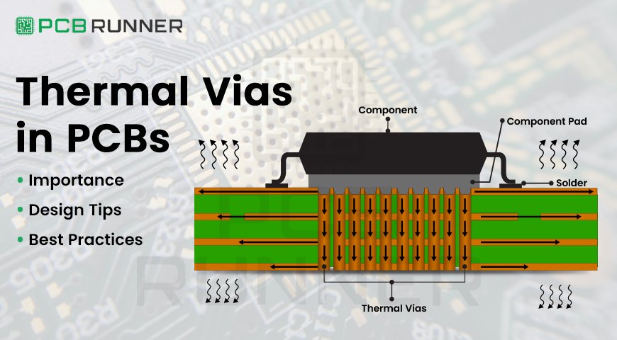
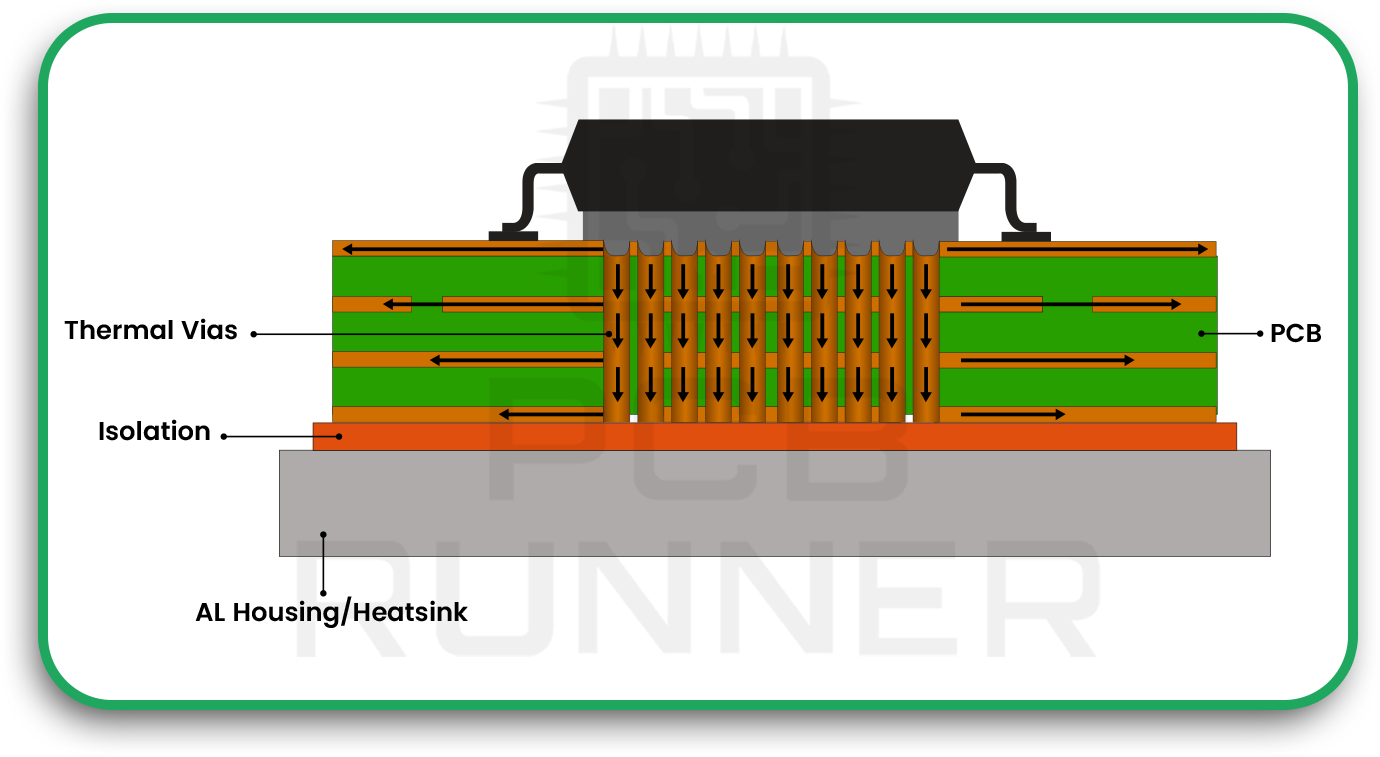
Thermal vias act as vertical heat pipes that carry excess heat from the top layer down to copper planes or heat sinks. In simple terms, they create a low-resistance thermal path so the heat can move freely.
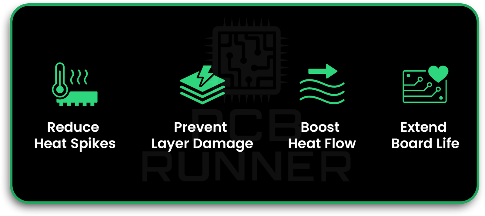
When designed correctly, thermal vias:
- Reduce temperature spikes around components
- Prevent delamination and solder joint fatigue
- Improve thermal conductivity across layers
- Help your board last longer under load
That’s the practical side of heat dissipation in PCBs, and it’s why so many PCB fabrication projects in Europe now treat thermal design as a core step in layout.
The Nature of Heat in PCBs
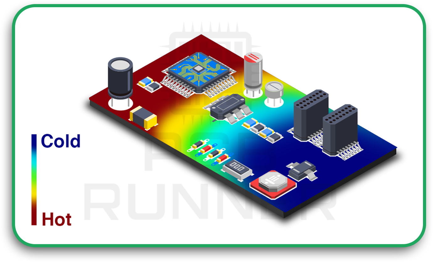
When components draw current, they release energy as heat. This heat travels through copper and laminate layers before reaching the surface or external cooling systems. But different materials have different thermal conductivities, copper is good, epoxy resin not so much.
That mismatch is why localised “hot zones” appear. Over time, these hotspots can cause warping, trace damage, or even electrical drift in precision circuits. The solution is a controlled thermal path, and vias offer precisely that.
Role of Thermal Vias in Heat Dissipation in PCBs
Think of thermal vias as metal straws inside your board. They connect the heat source on the surface to the inner copper layers that spread it out. The more vias you have, the easier it is for heat to find a way out.
Designers often place them under power devices like MOSFETs or voltage regulators, and in LED modules where light output can drop with rising temperature. Arrays of small vias do the job far better than one or two large ones. That’s because multiple contacts distribute heat more evenly.
PCB Runner’s engineering team is here to create thermally balanced designs for complex assemblies so contact our sales engineers today at sales@pcbrunner.com.
Impact on Reliability and Performance
Good PCB thermal management keeps the board at a stable temperature, which means your components stay within safe operating ranges. When parts run cooler, they behave predictably and have longer service lives.
On the flip side, neglecting thermal vias can create performance issues like signal distortion, expansion stress, or even component detachment. Temperature swings also weaken solder joints, a common reason why devices fail after only a few months.
Simply put, keeping the board cool keeps your product dependable.
Cost and Manufacturability Considerations
Adding hundreds of tiny vias might sound like it drives up costs, but here’s the thing, it often saves money later. Repairing a failed product costs far more than adding vias during the design phase.
A skilled PCB manufacturer in Europe will balance thermal performance with manufacturability. Drill size, spacing, plating thickness, and the number of layers all affect how easily those vias can be fabricated without adding delays or defects.
So, when designing your board, talk to your fabricator early. Their input can help you get the thermal results you want without overspending.
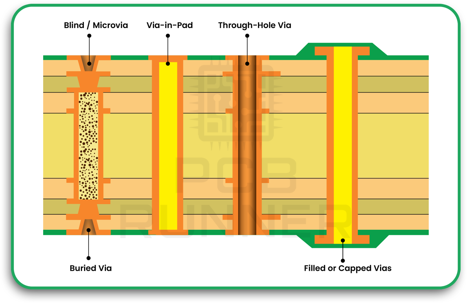
Types of Thermal Vias and When to Use Them
Standard Through-Hole Vias
These go from the top to the bottom of the board, carrying heat across every layer. They’re reliable, cost-effective, and widely used in high-power boards.
Via-in-Pad Vias
Here, the via sits right inside the component pad. This design helps transfer heat directly from the device to the copper layer underneath. It’s great for compact layouts where space is tight.
Micro Vias
Micro vias connect only between adjacent layers. They’re common in HDI (High Density Interconnect) designs and are effective where board thickness limits deeper drilling.
Filled or Capped Vias
Some vias are filled with copper or resin and then capped. This keeps solder from leaking during reflow and ensures a smooth surface for assembly.
When Vias Are Less Effective
They won’t help much if the board lacks solid copper reference planes or if the vias are isolated from primary power traces. You always need good thermal connectivity for them to work.
Key Design Guidelines for Thermal Vias
Let’s break it down with clear, practical tips you can apply to any project:
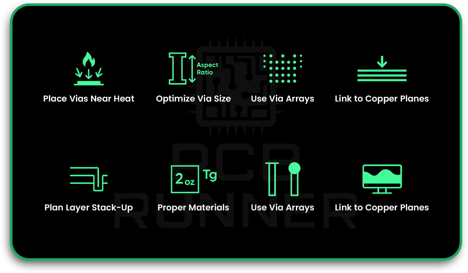
1. Place Vias Close to Heat Sources
The shorter the distance between the source and the via, the better. Put them under chips, near resistors, or along MOSFET legs.
2. Choose the Right Size and Aspect Ratio
Vias that are too small trap air pockets, which reduce heat flow. Use drill sizes around 0.2 to 0.3 mm and keep the aspect ratio within your fabricator’s limits.
3. Use Multiple Vias Instead of Fewer Big Ones
An array of small, evenly spaced vias improves thermal conduction more than a few large ones.
4. Connect to Copper Planes and Sinks
Always tie vias to ground or internal copper planes. More copper equals more thermal mass, which helps spread and absorb heat.
5. Plan Your Layer Stack-Up Early
You can’t fix thermal routing after the final layout. Define where the heat will flow and how inner layers share it early on.
6. Pick the Right Materials and Copper Weight
High-Tg laminates and 2 oz copper layers are common for boards that run hot. These materials handle thermal cycling better during operation.
7. Decide Whether to Tent or Plug Vias
Tenting keeps solder from entering the via. Plugging with epoxy or filling ensures a smooth surface when mounting components.
8. Verify with Simulation
Many PCB manufacturers in Europe use thermal simulation tools to check temperature distribution. If you have access to these tools, use them to visualise how your layout behaves before PCB fabrication.
Best Practices for Implementation
Start with thermal planning before you begin routing. Once the layout is done, it’s hard to go back and add proper cooling paths.
Combine your thermal vias with other cooling solutions like thermal pads, heat sinks, or fans. The goal is steady temperature, not just temporary fixes.
Work with your fabricator’s design guidelines so that what you create can actually be built. A manufacturable board saves both time and rework.
Always keep testing in mind. Leave some open zones for thermal probes and inspection points. Clear documentation of your thermal via strategy also helps the fabrication team understand your priorities.
Our design experts at PCB Runner help you validate your thermal strategy with in-depth simulation and DFM analysis.
Common Pitfalls You Should Avoid
Even experienced designers run into problems with thermal vias. Here are some you can sidestep:
- Using too few vias under power packages
- Forgetting to connect vias properly to inner planes
- Ignoring the layer copper thickness while planning the heat flow
- Placing vias so close that drilling becomes unreliable
- Failing to label filled or tented vias in the PCB fabrication notes
Each one can slow down production or cause heat issues later. Catching them early can save entire batches from scrap.
Quick Review Checklist Before Submitting Your Design
Before sending your files to your PCB manufacturer in Europe, check these points:
- Thermal vias under key heat-generating parts
- Appropriate number and spacing of vias
- Correct via fill or tenting details noted in drawings
- Strong copper connection from via barrels to planes
- Completed thermal simulations or test results attached
This final pass helps catch mistakes that software tools might miss.
Conclusion
Thermal vias might be tiny, but they make a big difference in how well your PCB handles stress and heat over time. When planned with care, they keep your design stable, safe, and long-lasting.
PCB Runner has built its reputation in the UK and across Europe by helping designers improve reliability through smarter heat control. Whether you’re developing power electronics, LED drivers, or compact IoT boards, smart thermal via design ensures your PCB stays calm, efficient, and ready for the field.
In the end, good thermal management isn’t about adding a few vias. It’s about thinking ahead, choosing materials, patterns, and fabrication methods that work together for the long run.
FAQs
- What do thermal vias do in PCB fabrication in Europe?
They transfer heat from components to internal copper layers or heat sinks, helping manage temperature during PCB fabrication in Europe. That improves performance and reliability.
- How many vias should I use for heat dissipation in PCBs?
That depends on component size and power level. A PCB manufacturer in Europe often recommends several small vias under each hot component for steady temperature control.
- Can poor via design in PCB layouts cause failure?
Yes. If the vias are too small, too few, or not connected to copper planes, heat can’t escape properly. This weakens solder joints and reduces lifespan.
- Does adding thermal vias increase the cost of PCB fabrication?
Slightly, but it’s worth it. The added cost during fabrication is small compared to the savings from improved reliability and fewer failures.
- What materials improve PCB thermal management in Europe?
High-Tg laminates, aluminium-backed boards, and thick copper layers are all good choices for better heat dissipation in PCBs made by manufacturers in Europe.