
Have you thought about the reasoning behind the differences in thickness among the copper lines on printed circuit boards (PCBs)? The thicker and thinner copper lines are referred to as PCB traces. Similar to the way roads in a city transport vehicles, traces on a PCB transport electrical signals. The thickness of these traces and the distance between them significantly influences the effectiveness of PCB design.
While the majority of you might not be deeply interested in electronics, PCB printed circuit board assembly, or the processes behind a circuit board supplier in the UK, you are likely to notice that there are design rules and restrictions that need to be observed during board construction. In this blog, we will explain these rules and design restrictions for you in a way that can be easily digested, even for a beginner.
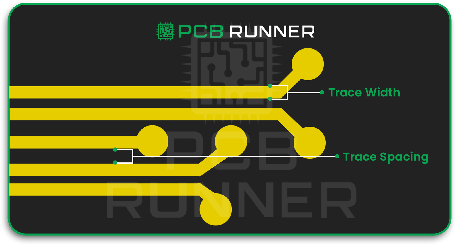
Why Does PCB Trace Width Matter?
Consider a PCB trace to be a water pipe. A narrow pipe will not be able to transport water easily, similar to the way a narrow trace will impede the flow of electrical current due to resistant heat. Excess heat can damage the board.
For this reason, PCB designers order the current capacity of the PCB trace width before finalizing the width of the trace. Choosing the right trace width keeps the PCB functional and ensures all signals are processed efficiently.
Key reasons why trace width matters:
- Heat control – For the efficient handling of current, wider traces are less prone to overheating.
- Signal quality – Correct trace width minimizes noise and interference.
- Durability – Damage to the copper during PCB production in the UK is minimized.
- Compliance – Manufacturing and safety standards are met.

What Is PCB Trace Spacing and Why Is It Important?
As with roads, traces on a PCB require distance between lanes, which in this case is called trace spacing. If lanes are too closely spaced, vehicles may collide. On a PCB, with traces spaced too closely, electrical signals may “leak” between traces. This effect, called crosstalk, can lead to short circuits.
Good spacing:
- Refrains from creating shorts and sparks between signals.
- Reduces interference between signals.
- Helps meet safety regulations for high-voltage designs.
These spacing rules are determined largely by the voltage level and the PCB production method utilized in the UK.
How to Determine PCB Trace Width
There is no need to make estimations as there are tools such as a pcb trace width calculator which will do the job for you. These calculators take into consideration:
- The Current (Amps) the trace will carry
- The copper thickness on your board
- The temperature rise you can allow
Take for example a 1 amp trace. With 1 ounce copper thickness, calculators will help you determine the width to keep it safe.
Tip: Safety margins should be added. Wider traces will accommodate for surges just like wider roads which are better equipped for uncontrolled traffic increases

How to Decide PCB Trace Spacing
As a rule of thumb, the amount of space is to do with voltage preventing a jump. The higher the voltage, the greater the distance.
There is a common standard:
- Low voltage (<30V): 0.1 mm spacing is often fine.
- Medium voltage (30V–100V): 0.6 mm or more.
- High voltage (>100V): Several mm, always comply with safety standards.
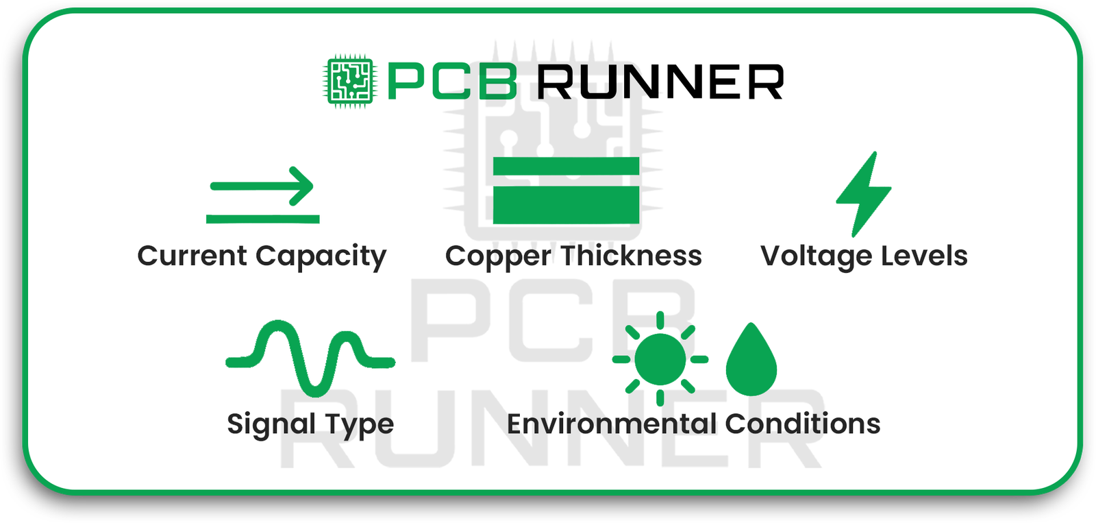
Factors Affecting PCB Trace Width and Spacing
Every printed circuit board (PCB) is unique and requires specific factors to be considered when designing PCB traces. These include:
Current Capacity
A trace must be ‘wider’ to manage ‘more’ current.
Copper Thickness
A thicker copper layer is able to manage more current without overheating.
Voltage Levels
More spacing is required for higher voltages.
Signal Type
High-speed signals require careful width and spacing to avoid cross talk.
Environmental Conditions
Will the PCB be exposed to high temperatures or moisture? That requires wider traces and larger spacing.
Using PCB Trace Current Calculators
A pcb trace current calculator is an important tool for firms to take the guess work out and ensure the design is functional. You input:
- Current Load
- Copper Thickness
- Maximum allowable temperature rise
Common Mistakes in PCB Trace Design
- Narrow traces leading to overheating and damage.
- Ignoring spacing rules leading to short circuits or signals interfering with each other.
- Oversights such as sharp 90° corners or the extraction of manufactural limits weaken a board.
Prior to submitting your design for printed circuit board (PCB) assembly, ensure it is thoroughly checked for any possible mistakes.
If you’d like expert design reviews before production, our engineers at PCB Runner can help you optimize your layout and avoid costly errors. Contact us at sales@pcbrunner.com to discuss your project.
Tips for Perfect PCB Trace Width and Spacing
Designing and manufacturing printed circuit boards is a complex process, and faxing ensures success.
- Make sure to use a trace width calculator at the beginning of the design process.
- Make sure to check the manufacturer’s minimum trace width and spacing.
- Make sure the width of power traces is greater than the minimum.
- Make sure to keep high-speed signal traces both short and well-spaced.
- In order to reduce interference, keep analog and digital traces separate.
- Increase the clearance for high-voltage circuits.
- Always run DRC prior to production.
Why These Decisions Matter for PCB Production in the UK
When working with circuit board suppliers UK, providing accurate width and spacing details makes the manufacturing process smoother. It also ensures your design passes quality checks quickly.
Consequences of Neglecting Design Best Practices:
- The board may encounter failures during the testing phase.
- You may incur expensive redesign expenses.
- There may be production delays.
- Correct PCB trace width and spacing regulations save resources and finances.
Final Thoughts
While selecting the PCB trace width and spacing may seem trivial, it is the core of any dependable design. Be it a homemade pcb printed circuit board assembly or when collaborating with pcb production UK professionals, adhering to the guidelines will enhance the circuit’s durability and optimize its performance.
The positive aspect is that with the advancements of technology, guessing is now an obsolete practice. Smart and safe decisions can now be made utilizing trace width and current calculators, alongside IPC’s standards.
Use of IPC trace current and width calculators or CAD software will further support these decisions. While it is advisable to reach out to design professionals, manufacturers, and in this case, PCB Runner, who are grounded in production reality, can offer invaluable suggestions. Such collaborations will ensure the designs are realizable and align with production capabilities.