
Designing electronics for healthcare is unlike creating boards for consumer gadgets. A single failure can compromise patient safety or lead to costly regulatory delays. This guide walks you through a proven, end-to-end process for medical device PCB design from concept to production by ensuring compliance and reliability.
Whether you’re comparing printed circuit board manufacturers, seeking custom PCB assembly, or planning a full turnkey assembly for high-stakes medical equipment, these steps will help you meet strict quality standards and reduce time to market.
And if you need expert support at any stage, our team is here at sales@pcbrunner.com to help you move from design to production with confidence.
Let’s start with a question.
If you were designing a medical device, something that a patient’s life might depend on, how much room would you leave for error?
Probably none.
That’s the reality when working with medical device PCB design. These boards go into equipment like heart monitors, defibrillators, MRI scanners, and portable diagnostic tools. In all those cases, failure isn’t just inconvenient. It could be dangerous.
Here’s the thing: designing a PCB for medical devices is not the same as designing one for a smartphone or a smart home gadget. The technical side is more demanding. The regulations are tighter. The margin for error? Almost zero.
So let’s walk through the process step-by-step, from the first sketch to the point where the board is ready to be assembled and tested. I’ll keep it simple, clear, and practical so that you can use this as a real checklist, not just another “how-to” you forget five minutes later.
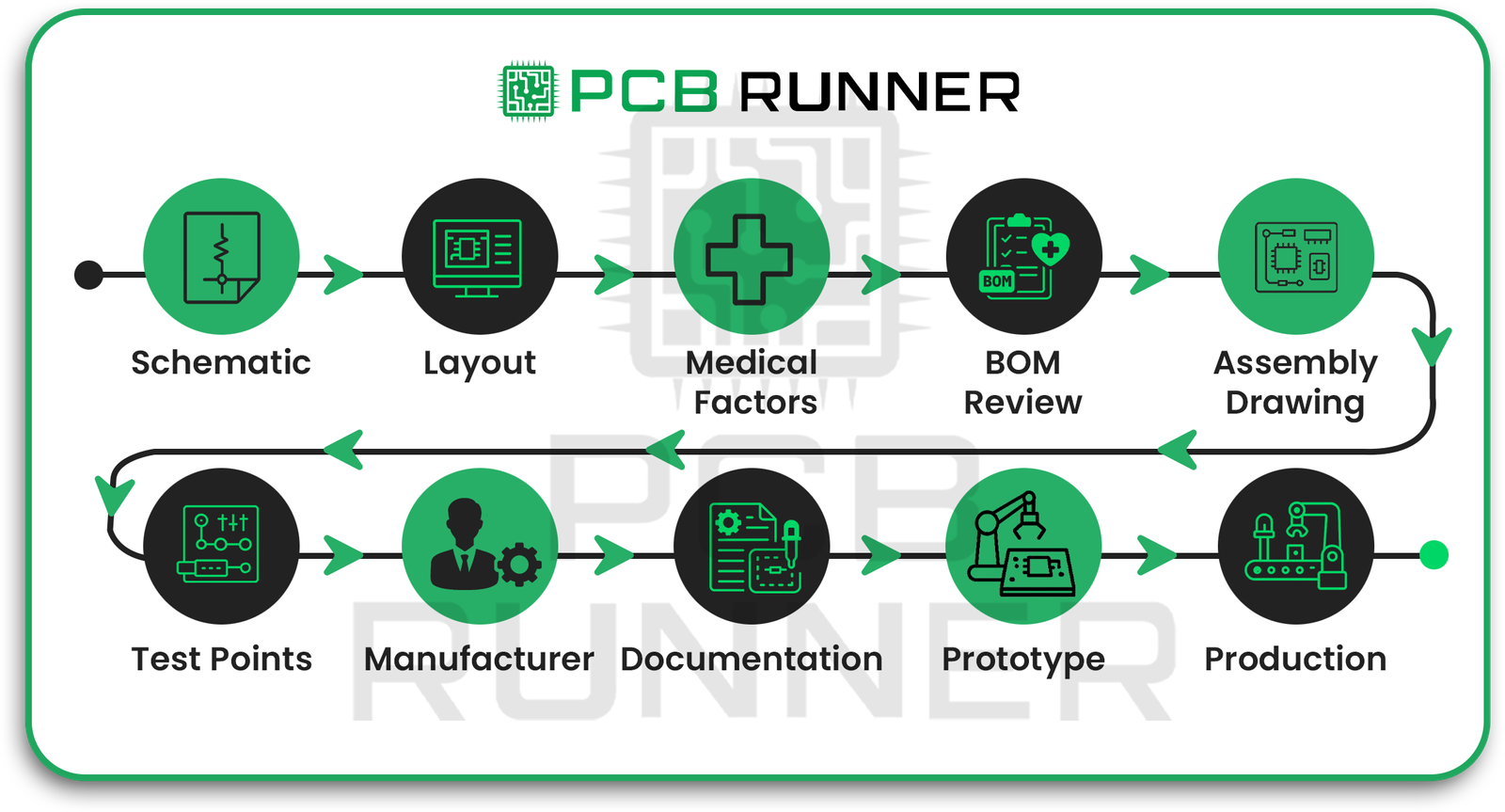
Step 1: Draw the Schematic
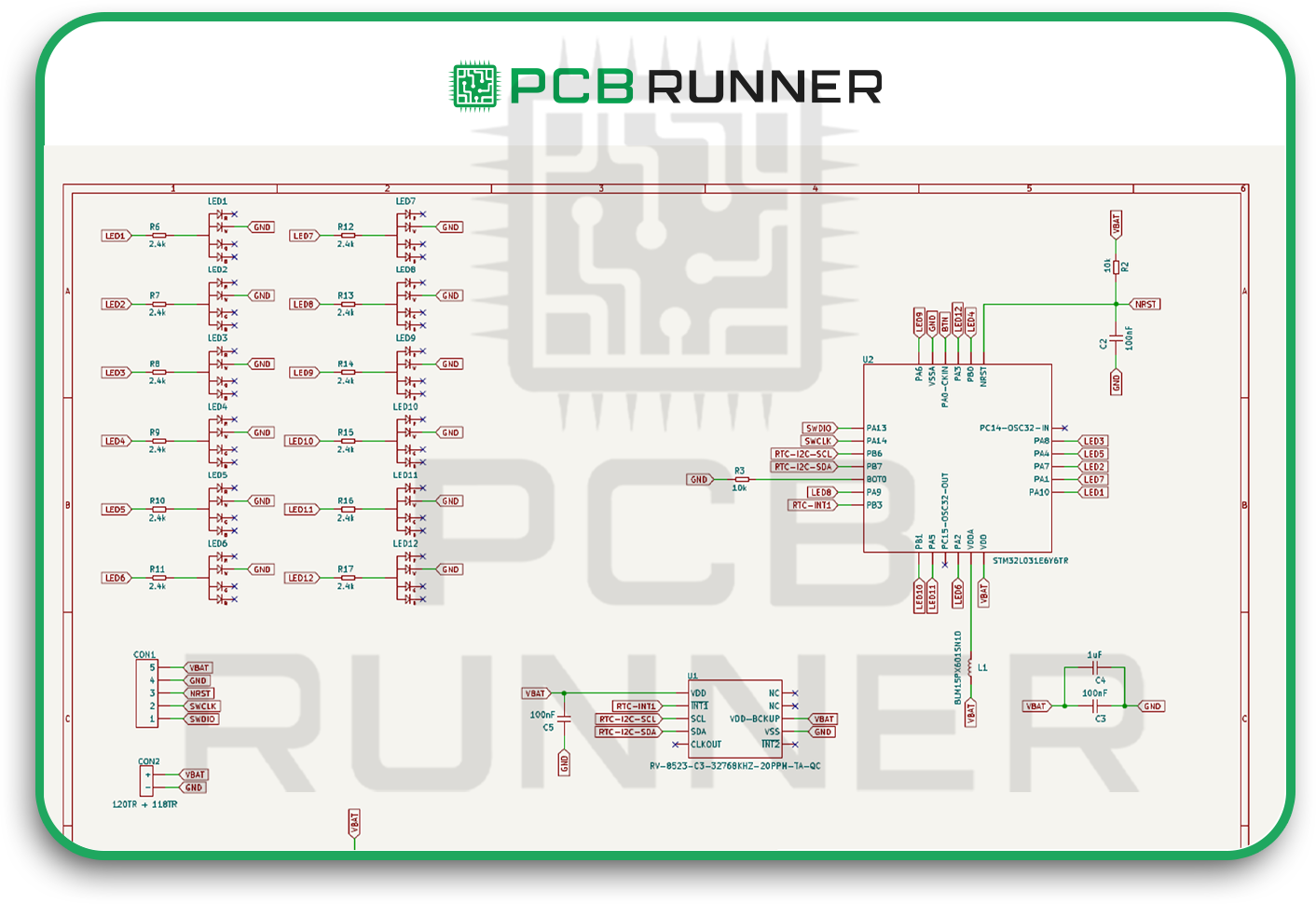
Every board starts with a schematic. Think of it as your map showing how each component connects.
When you’re creating a schematic for PCB assembly for medical purposes, you want to include key details right from the start:
- The material type you expect to use for the PCB.
- The power needed for your design.
- All essential components, placed and connected logically.
Don’t rush this part. Mistakes here will haunt you later in the layout stage, and fixing them later costs time and money.
Step 2: Design the PCB Layout
Once you have the schematic, you move to the layout stage. This is where you decide where each component physically sits and how the copper traces connect them.
Most designers use CAD software for this. You’ll import your schematic, then start arranging components in a way that keeps signal paths short and clean.
For medical device PCB assembly, noise and signal clarity are critical. That means:
- Avoid routing high-speed signals near sensitive analogue lines.
- Keep critical signals short.
Plan your ground and power planes early to avoid last-minute patch jobs.
Step 3: Pay Attention to Critical Medical PCB Factors
This is where many engineers miss details that matter in regulated industries.
Here’s what you should focus on:
- Component choice: Stick to parts that have proven long-term reliability. Don’t gamble on untested suppliers.
- Split power planes and proper grounding: Splitting power planes and adding multiple ground layers helps reduce interference.
- Clear silkscreen markings: Make component labels unambiguous so assembly teams can find precisely what goes where.
- Signal-to-noise ratios: Medical devices often deal with very low, sensitive signals. Noise on those lines can cause incorrect readings or insufficient data.
If you get just one thing from this section, let it be this: in medical electronics, stability is everything.
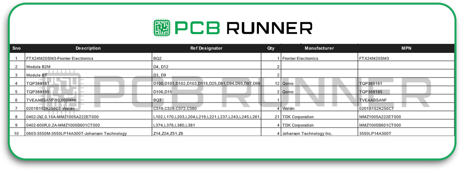
Step 4: Review the Bill of Materials (BOM)
The BOM is your recipe for building the board. In medical device PCB design, it’s also part of your compliance record.
What to do here:
- Confirm every part number and supplier is correct.
- Read each datasheet, don’t assume a part will work because it looks right.
- Create an alternate component list in case your first-choice parts are unavailable.
A complete, accurate BOM speeds up full turnkey assembly because there’s no back-and-forth with the manufacturer on missing or mismatched components.
Step 5: Create an Assembly Drawing
The assembly drawing shows exactly how your finished board should be built.
Think of the assembly drawing as the instruction manual for your custom PCB assembly team. It should include:
- Component outlines and reference numbers.
- Polarity markings were required.
- Notes about special handling or soldering requirements.
A good assembly drawing removes guesswork and ensures that every medical device PCB assembly looks and works the same.
Step 6: Add Test Points
Testing is non-negotiable in medical electronics.
Adding clear, accessible test points during design helps technicians check voltages, signals, and performance without damaging the board. This improves test speed, reduces errors, and makes future troubleshooting easier.
Skipping test points is one of the most common mistakes in PCB design, and one of the costliest to fix later.
Step 7: Work Closely with Your Manufacturer
Here’s what this really means: pick your printed circuit board manufacturers UK partner early, and involve them in the design process.
Why? Because a manufacturer experienced in PCB assembly for medical devices will:
- Suggest better materials that meet medical compliance.
- Flag design features that might raise costs or cause delays.
- Help with documentation for ISO 13485 requirements.
A good medical device PCB isn’t just designed well, it’s also built by people who understand the regulations and demands of healthcare electronics.
Step 8: Meet Regulatory and Quality Documentation Needs
You can’t sell a medical device without paperwork, especially in the UK, EU, or US.
At a minimum, expect to prepare:
- Design history and change records.
- Traceability logs for all components.
- Test records and inspection reports.
- Verification/validation documentation.
An experienced manufacturer offering a complete turnkey assembly can help generate and store these records for you.
Step 9: Prototype and Test Thoroughly
Never jump into mass production without building prototypes first.
Prototypes let you:
- Verify your schematic logic.
- Catch signal integrity issues.
- Confirm heat dissipation is adequate.
- Validate assembly instructions and BOM accuracy.
With medical device PCB assembly, multiple prototype rounds aren’t overkill, they’re a smart investment.
Step 10: Move to Production with Full Turnkey Assembly
When the design is solid and testing is complete, it’s time for production.
Choosing a full turnkey assembly streamlines things. It means the manufacturer handles:
- Board fabrication.
- Component sourcing.
- PCB assembly.
- Testing and inspection.
- Final packaging.
This approach saves time and keeps the process consistent, which is crucial for PCBs for medical devices.
Step 11: Focus on Long-Term Reliability
Remember, many medical devices run for years without interruption. That means your PCB must be durable enough to handle long service cycles, cleaning cycles, possible heat stress, and occasional mishandling.
Ask your manufacturer about:
- Conformal coating for moisture protection.
- High-reliability solder joints.
- Specialised component mounting for vibration resistance.
Why the Right Partner Matters
Choosing the wrong manufacturer can lead to delays, compliance issues, or even device failures. That’s why partnering with PCB Runner is critical. We specialize in custom PCB assembly for high-stakes industries like medical devices, offering complete turnkey solutions that meet the strictest quality standards. Get in touch with our team today to ensure your medical device PCBs are built with precision, compliance, and reliability from the start.
Working with the wrong manufacturer can cause delays, compliance failures, or worse, device malfunctions. Companies like PCB Runner focus on custom PCB assembly for precisely these high-stakes situations.
They understand the nuances of medical device PCB design, provide complete turnkey assembly, and ensure that every PCB for medical devices meets strict quality standards.
Wrapping It Up
Designing a medical device PCB isn’t just electrical engineering. It’s a careful mix of technical precision, regulatory compliance, and practical assembly planning.
Get the schematic right. Plan your layout to minimise noise. Double-check the BOM. Add test points. Work with a manufacturer who understands the regulatory side as well as the engineering.
Do that, and your medical device PCB assembly will be ready to perform exactly as needed, every time.
And once the boards are built, don’t overlook professional labelling. Partnering with a supplier like Dura Fast Label helps ensure your finished device looks as professional as it performs, with labels that last through use, cleaning, and transport.
If you follow this step-by-step guide, you’ll not only meet the technical and legal requirements for medical PCBs, you’ll also end up with a design you can trust, and so can your end users.
That’s the real goal.