
The Internet of Things (IoT) is changing the way we live and work. From smart thermostats and fitness trackers to industrial sensors and connected vehicles, IoT devices are everywhere. But what makes these devices possible? At the heart of every IoT device is a carefully engineered printed circuit board (PCB). The right PCB design and production choices are what allow IoT devices to be small, efficient, and reliable.
If you want to understand where IoT is heading and how to build devices that stand out, you need to know how Multilayer PCB, Flex and Rigid PCB, and smart PCB production methods make it all work. Let’s break down the key technical details and best practices for designing PCBs for the Internet of Things.
Understanding IoT PCB Requirements
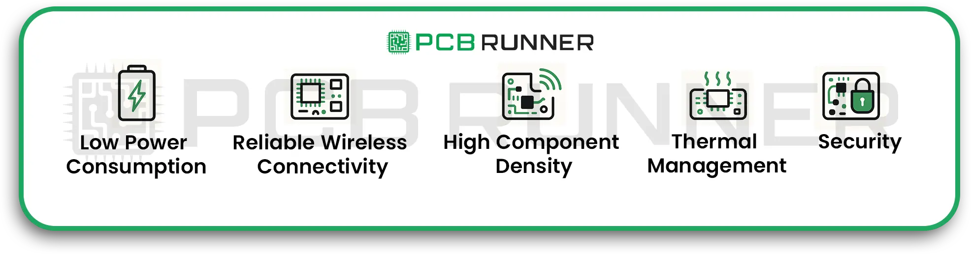
IoT devices come in many forms, but they all have a few things in common. They need to be compact, often run on battery power, and must connect wirelessly. That means the PCB inside must be designed for low power, high density, and strong wireless performance.
Here’s what you need to focus on when working with IoT PCB design:
- Low power consumption: Most IoT devices use batteries. The PCB must help minimise power draw to extend battery life.
- High component density: Space is limited, so you need to fit more components into a smaller area.
- Reliable wireless connectivity: The board must support antennas and RF circuits without causing interference.
- Thermal management: Even small devices generate heat. Good PCB design keeps temperatures under control.
- Security: Many IoT devices handle sensitive data. Hardware security features can be built into the PCB.
Multilayer PCB: The Foundation for Complex IoT Devices
As IoT devices get smaller and more powerful, a single-layer PCB often isn’t enough. Multilayer PCB technology stacks several layers of circuitry, separated by insulating material, into one compact board. This approach allows you to:
- Route more signals in less space
- Separate analogue and digital signals to reduce interference
- Improve power distribution and grounding
- Support high-speed data and wireless signals
For example, a smart thermostat might use a Multilayer PCB to keep the Wi-Fi, processor, and sensor circuits separate, reducing noise and improving reliability2. In industrial IoT, Multilayer PCBs are essential for handling complex control and communication tasks.
Flex and Rigid PCB: Adapting to Any Shape or Space
IoT devices don’t always come in neat rectangles. Wearables, medical sensors, and automotive IoT often need PCBs that bend, fold, or fit into unusual spaces. That’s where Flex and Rigid PCB designs come in.
- Flex PCBs are made from flexible materials, allowing them to bend and twist without breaking. They’re perfect for devices that need to fit into tight or curved spaces.
- Rigid-Flex PCBs combine rigid sections (for mounting chips and connectors) with flexible sections (for folding or bending). This design reduces the need for connectors and cables, saving space and improving reliability.
Flex and Rigid PCB technology lets you design devices that are lighter, more durable, and more comfortable to wear or use.
PCB Production for IoT: What Matters Most
The best IoT devices depend on high-quality PCB production. Here are the most important factors to consider:
- Material selection: Choose materials that match your device’s needs. For example, flexible substrates for wearables or high-frequency laminates for wireless modules9.
- Precision manufacturing: IoT PCBs often use High-Density Interconnect (HDI) techniques, such as microvias and fine trace widths, to fit more into less space.
- Quality control: Consistent production is key. Even small defects can cause big problems in small devices.
- Customisation: Every IoT application is different. PCB production should allow for custom shapes, sizes, and features.
Best Practices for PCB Design for the Internet of Things
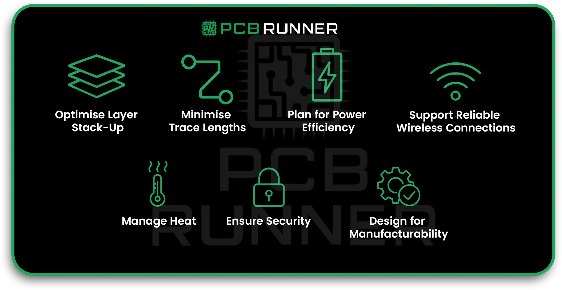
To get the most from your IoT PCB, follow these proven design strategies:
1. Optimise Layer Stack-Up
Use multiple layers to separate power, ground, and signal traces. This reduces noise and improves signal integrity, especially for wireless and high-speed circuits.
2. Minimise Trace Lengths
Shorter traces mean less signal loss and a lower risk of interference. Keep sensitive signals as short as possible, and use controlled impedance routing for high-speed or RF signals.
3. Plan for Power Efficiency
Choose low-power components and use power-saving design techniques. For example, use sleep modes for microcontrollers and sensors, and minimise the number of active circuits at any time.
4. Manage Heat
Even small IoT devices can get hot. Use thermal vias, copper pours, and a good component layout to spread and remove heat.
5. Support Reliable Wireless Connections
Keep antennas and RF circuits away from noisy digital signals. Use proper grounding and shielding to reduce electromagnetic interference (EMI).
6. Ensure Security
If your device handles sensitive data, consider adding hardware security modules or secure elements directly to the PCB.
7. Design for Manufacturability
Follow DFM (Design for Manufacturability) guidelines to make sure your board can be produced at scale, with minimal errors and rework.
Real-World Example: Smart Home Sensor
Let’s say you’re designing a smart home sensor. You’d likely use a Multilayer PCB to separate the power, processor, and wireless circuits. If the sensor needs to fit in a small or curved case, a Flex PCB makes sense. You’d keep trace lengths short, use microvias for high density, and make sure the antenna is isolated from digital noise. The result? A sensor that’s small, reliable, and lasts for years on a single battery.
Challenges in IoT PCB Design
Designing PCBs for IoT isn’t without its hurdles:
- Signal integrity: High-frequency signals are sensitive to noise and interference. Careful routing and grounding are a must.
- Component placement: With so many parts in a small space, placement is critical for both performance and manufacturability.
- Testing and validation: Each device must be tested for power use, wireless range, and durability.
- Cost control: Advanced features like Multilayer PCB and Flex and Rigid PCB add cost. Balance performance with budget for your application.
The Future of IoT PCB Design
As IoT continues to grow, PCB design and production will keep evolving. Expect to see:
- Even higher density layouts, thanks to new HDI and micro via technology
- More use of Flex and Rigid PCB designs for wearables and medical devices
- Better integration of security and wireless features at the hardware level
- Smarter, more automated PCB production for faster turnaround and lower costs
Key Takeaways
- IoT devices depend on advanced PCB design and production for performance, size, and reliability.
- Multilayer PCB and Flex and Rigid PCB technologies are essential for fitting more features into smaller, more complex devices.
- Good PCB design for the Internet of Things focuses on power efficiency, signal integrity, thermal management, and manufacturability.
- As IoT grows, so will the need for innovative PCB production methods and materials.
If you’re building for the future, start with the right PCB. It’s the foundation that makes every connection possible.
Conclusion: PCB Runners and the Connected Future
The Internet of Things is transforming every industry, from smart homes to healthcare to industrial automation. At the heart of this transformation are advanced PCBs—especially Multilayer PCB, Flex and Rigid PCB, and rigid HDI substrates—that make it possible to pack more features, better connectivity, and higher reliability into smaller, more efficient devices.
Careful PCB design for Internet of Things applications is essential for meeting the strict demands of power efficiency, wireless performance, and durability that modern IoT devices require.
PCB Runners stands out as a leader in this space, delivering PCB solutions that support the unique needs of IoT innovation. Their expertise in rigid HDI PCB fabrication, power distribution, and signal integrity ensures that your IoT devices are not only compact and efficient but also robust enough for real-world use.