The Limitations of Standard PCB Technology
Printed circuit boards, or PCBs, are essential to the modern electronics industry because they enable high-density circuit and component integration. Despite the tremendous advancements in recent decades, PCB technology still has drawbacks.
Designers and engineers must identify these constraints in order to guarantee that they will not incur any costs during the manufacturing assembly of the product.
In this blog, we will discuss the constraints of standard PCB technology related to size, materials, performance, and manufacturing capability, including how HDI PCB manufacturing can help overcome some of these challenges. Whether you are a beginner or have experience, being aware of these limitations helps you make informed decisions during the PCB design process.
Common Limitations of Standard PCB Technology
As much advancement PCB designs and models have made over the years, they are still limited by various specific issues that were mentioned earlier that designers must not ignore.
Thickness and Dimensions of PCB Models
- Board Dimensions: As PCBs become smaller and more compact, it becomes challenging to fit all components into a tight space without compromising functionality. This often leads to issues with component spacing and routing, particularly with HDI PCB designs.
- Board Thickness: PCBs are manufactured with a specific thickness in mind, and increasing the thickness beyond the standard can affect the flexibility, weight, and cost of manufacturing.
Material Limitations
- Limited Material Choices: People often use FR4 (fiberglass epoxy) to fabricate PCBs, and while that is fine and dandy, it is not the most optimal option for high-load performance requirements that have very stringent criteria, such as responding quickly to high frequency or being heat resistant.
- Thermal Management: Super-thin standard PCB models do a poor job regulating temperature. If they are not actively managed, overheating becomes the norm, especially with high-power components. Even within the lower ranges, one can only imagine the capacity potential.
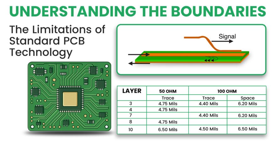
Signal Integrity and High-Speed Performance
- Signal Interference: As components on a PCB get smaller and packed tighter together, signal interference becomes an increasing factor to consider. High levels of crosstalk and EMI can undermine the quality of the signal in high-frequency designs.
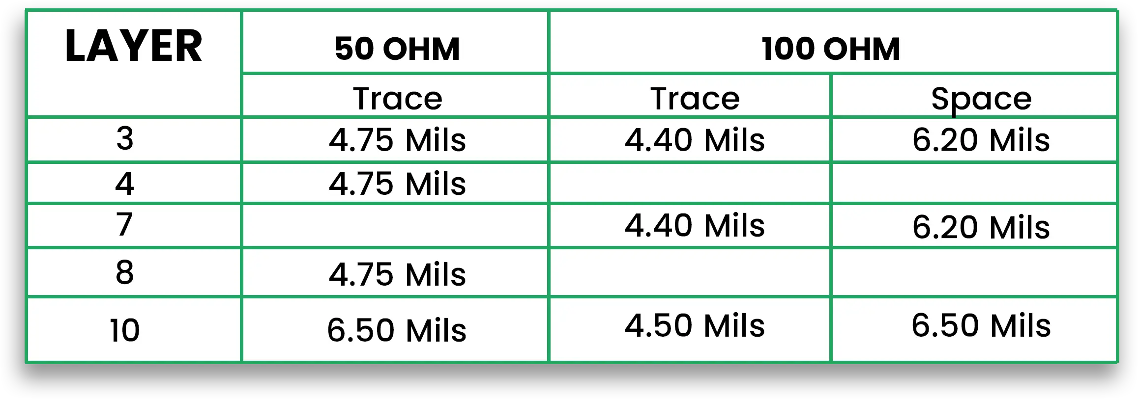
- Impedance Control: Traditional PCB layouts are not very good at controlling the impedance on one or several critical high-speed transmissions. Being off in terms of impedance creates a reflection in the signal and, subsequently, the loss of the signal or its distortion.
Manufacturing Constraints
- Resolution Limits: The finer the trace width and the component pads, the harder it is to make a PCB. Conventional manufacturing tools may not be able to provide the necessary precision for HDI PCB manufacturing and microelectronic PCBs.
- Via Limitations: Some of the restrictions imposed by standard PCBs on the sizes of vias and their locations may impact the routing of signals and power distribution, especially in multi-layer PCBs.
Component Density and Routing
- Routing Complexity: As additional components and layers increase, the HDI PCB design becomes more complex, and routing becomes more challenging as well. The interconnection of components can require multiple layers of routing, which adds to the board’s cost and complexity.
- Component Size: Size Reduction is a popular trend in electronics. However, standard PCB technology usually does not accommodate the very tiny components needed in gadgets such as phones or all sorts of wearables.
Benefits and Application
These restrictions sound limiting, especially for design. However, grasping these restrictions helps you make better choices during the design stages.
Becoming aware of possible risks in the early stages helps one take measures to tackle them.
For example, the designer can use an alternate set of materials, make the gap between the components more significant, or investigate better technologies such as HDI PCB manufacturing.
By accepting these limitations, designers can improve their layouts, enhance manufacturability, and reduce the chances of failure.
Expert Opinion
Expert Insight by NASA: Limitations of PCBs
Printed Circuit Boards (PCBs) are crucial in modern electronics, but the failure to address their limitations may have severe implications. Failure in PCB design or manufacturing can result in a series of problems for manufacturers and end-users. Manufacturers will experience a delay in the time-to-market of their products, increased warranty costs, and reputational damage. Such failures can discourage customers from buying, decrease market share, and raise liability claims based on damages from faulty products.
For end-users, PCB failures often translate into personal injury risks, mission-critical operation losses, and costly repairs or replacements. Beyond direct costs, such failures can result in indirect financial burdens, such as increased insurance premiums, reputational harm, and a reduced competitive edge in the market.
These limitations highlight the importance of precise PCB design, rigorous testing, and adherence to quality standards to ensure reliability and mitigate potential failures.
Frequently Asked Questions
Q: What is the most critical drawback of utilizing FR4 in the construction of high-frequency PCBs?
A: High frequency and signal integrity retain a direct relationship, so an FR4 would be inappropriate due to its dielectric constant and loss tangent, which are relatively higher than what is deemed ideal.
Q: What role does the thickness of a PCB play in the optimal functioning of a device?
A: Increasing the thickness of the PCB can have multiple drawbacks. While it can reduce the overall board flex, it will also increase the weight, temperature, and rigidity, which may affect heat dissipation.
Q: Is it possible to enhance or retain a circuit performance while reducing the area occupied by a PCB?
A: Yes, but there are plenty of factors that must be considered. Small PCBs do require density components with smaller traces; however, some innovative methods can still be employed to retain the circuit’s signal integrity.
Conclusion
Understanding the limits of standard PCB technology is critical for achieving cost-effective and trustworthy designs. Awareness of these limitations should be established at the beginning of the design so that decisions can be made to increase the PCB’s efficiency.